EP2562836A1 - Actionneur piézo-électrique et son procédé de fabrication - Google Patents
Actionneur piézo-électrique et son procédé de fabrication Download PDFInfo
- Publication number
- EP2562836A1 EP2562836A1 EP11771868A EP11771868A EP2562836A1 EP 2562836 A1 EP2562836 A1 EP 2562836A1 EP 11771868 A EP11771868 A EP 11771868A EP 11771868 A EP11771868 A EP 11771868A EP 2562836 A1 EP2562836 A1 EP 2562836A1
- Authority
- EP
- European Patent Office
- Prior art keywords
- electrode
- piezoelectric
- piezoelectric actuator
- layer
- base substrate
- Prior art date
- Legal status (The legal status is an assumption and is not a legal conclusion. Google has not performed a legal analysis and makes no representation as to the accuracy of the status listed.)
- Withdrawn
Links
Images


Classifications
-
- H—ELECTRICITY
- H10—SEMICONDUCTOR DEVICES; ELECTRIC SOLID-STATE DEVICES NOT OTHERWISE PROVIDED FOR
- H10N—ELECTRIC SOLID-STATE DEVICES NOT OTHERWISE PROVIDED FOR
- H10N30/00—Piezoelectric or electrostrictive devices
- H10N30/20—Piezoelectric or electrostrictive devices with electrical input and mechanical output, e.g. functioning as actuators or vibrators
- H10N30/204—Piezoelectric or electrostrictive devices with electrical input and mechanical output, e.g. functioning as actuators or vibrators using bending displacement, e.g. unimorph, bimorph or multimorph cantilever or membrane benders
- H10N30/2041—Beam type
- H10N30/2042—Cantilevers, i.e. having one fixed end
-
- H—ELECTRICITY
- H10—SEMICONDUCTOR DEVICES; ELECTRIC SOLID-STATE DEVICES NOT OTHERWISE PROVIDED FOR
- H10N—ELECTRIC SOLID-STATE DEVICES NOT OTHERWISE PROVIDED FOR
- H10N30/00—Piezoelectric or electrostrictive devices
- H10N30/01—Manufacture or treatment
- H10N30/07—Forming of piezoelectric or electrostrictive parts or bodies on an electrical element or another base
- H10N30/074—Forming of piezoelectric or electrostrictive parts or bodies on an electrical element or another base by depositing piezoelectric or electrostrictive layers, e.g. aerosol or screen printing
- H10N30/076—Forming of piezoelectric or electrostrictive parts or bodies on an electrical element or another base by depositing piezoelectric or electrostrictive layers, e.g. aerosol or screen printing by vapour phase deposition
-
- H—ELECTRICITY
- H10—SEMICONDUCTOR DEVICES; ELECTRIC SOLID-STATE DEVICES NOT OTHERWISE PROVIDED FOR
- H10N—ELECTRIC SOLID-STATE DEVICES NOT OTHERWISE PROVIDED FOR
- H10N30/00—Piezoelectric or electrostrictive devices
- H10N30/01—Manufacture or treatment
- H10N30/08—Shaping or machining of piezoelectric or electrostrictive bodies
- H10N30/081—Shaping or machining of piezoelectric or electrostrictive bodies by coating or depositing using masks, e.g. lift-off
-
- H—ELECTRICITY
- H10—SEMICONDUCTOR DEVICES; ELECTRIC SOLID-STATE DEVICES NOT OTHERWISE PROVIDED FOR
- H10N—ELECTRIC SOLID-STATE DEVICES NOT OTHERWISE PROVIDED FOR
- H10N30/00—Piezoelectric or electrostrictive devices
- H10N30/80—Constructional details
- H10N30/85—Piezoelectric or electrostrictive active materials
- H10N30/853—Ceramic compositions
- H10N30/8542—Alkali metal based oxides, e.g. lithium, sodium or potassium niobates
-
- Y—GENERAL TAGGING OF NEW TECHNOLOGICAL DEVELOPMENTS; GENERAL TAGGING OF CROSS-SECTIONAL TECHNOLOGIES SPANNING OVER SEVERAL SECTIONS OF THE IPC; TECHNICAL SUBJECTS COVERED BY FORMER USPC CROSS-REFERENCE ART COLLECTIONS [XRACs] AND DIGESTS
- Y10—TECHNICAL SUBJECTS COVERED BY FORMER USPC
- Y10T—TECHNICAL SUBJECTS COVERED BY FORMER US CLASSIFICATION
- Y10T29/00—Metal working
- Y10T29/42—Piezoelectric device making
Definitions
- the present invention relates to a piezoelectric actuator that performs electrical control by using a piezoelectric material.
- a cantilever arm is attached to the surface of a base substrate.
- the arm includes a vertical wall portion serving as a cantilever support portion and having a wall surface orthogonal to the base substrate, and a horizontal wall portion supported by the vertical wall portion and having a wall surface parallel to the base substrate portion.
- a movable electrode is formed on the horizontal wall surface.
- a fixed electrode is formed on the inner wall of a cover portion that covers the arm.
- a lower electrode, a piezoelectric film, and an upper electrode are arranged in this order near the support side end of the horizontal wall portion of the arm. These components constitute a piezoelectric drive portion.
- a drive voltage is applied between the lower electrode and upper electrode of the piezoelectric drive portion, the piezoelectric film is distorted, the arm bends upwards, and the movable electrode comes into close proximity to the fixed electrode. In this way, as the distance between the movable electrode and the fixed electrode varies depending on whether or not a drive voltage is applied, the switching element functions as a switch or a variable capacitance element.
- the movable electrode, the arm, and the piezoelectric drive portion are formed separately. Therefore, there are a large number of components that constitute the switching element, which also increases the number of steps in the manufacturing flow for forming those individual components.
- a piezoelectric actuator includes a base substrate that has an insulating property, a fixed electrode that is formed in the base substrate, a lower electrode, a piezoelectric layer, an upper electrode, and a movable electrode.
- the lower electrode is an electrode for applying a piezoelectric drive voltage which is at least partially separated from the base substrate.
- the piezoelectric layer is formed on a side of the lower electrode opposite to the base substrate.
- the upper electrode is an electrode for applying the piezoelectric drive voltage which is formed on a side of the piezoelectric layer opposite to the lower electrode.
- the distance of the movable electrode to the fixed electrode varies as the piezoelectric layer is distorted by application of the piezoelectric drive voltage. In this configuration, at least a portion of the movable electrode is formed by the upper electrode or the lower electrode.
- the movable electrode itself has the function of an arm that bends, and hence the configuration is simplified. Further, the upper electrode or the lower electrode is partially included in the movable electrode, which further simplifies the configuration. Also, the fixed electrode is provided to the base substrate. Thus, no cover is required for the function of the electrical circuit, which also leads to simplification of the configuration.
- one end of the movable electrode is supported by a stacked structure portion that includes the lower electrode, the piezoelectric layer, and the upper electrode.
- This configuration illustrates a specific configuration of the support column for the movable electrode.
- the configuration according to the present invention can bring about desired changes in the movable electrode without separately providing an arm in addition to the movable electrode.
- the movable electrode is formed by the upper electrode.
- the upper electrode doubles as the movable electrode, and also serves as an arm that bends.
- the configuration is further simplified as a result.
- the upper electrode is formed later in the manufacturing flow than the piezoelectric layer, and hence not affected by the manufacturing process conditions applied to the piezoelectric layer. Therefore, the range of choices for the material of the movable electrode that doubles as the upper electrode increases. Accordingly, a suitable material can be easily selected in accordance with the product specifications, cost, and so on.
- a dielectric layer is formed between the fixed electrode and the movable electrode.
- the piezoelectric actuator As the specific structure of the piezoelectric actuator, a dielectric layer is provided between the fixed electrode and the movable electrode. The presence of this dielectric layer ensures that the fixed electrode and the movable electrode do not come into direct contact with each other. Therefore, the piezoelectric actuator can be used both as, for example, a high frequency switch for frequencies in the range of 50 MHz to 10 GHz, and as a high frequency capacitance element. Also, as compared with a case where the fixed electrode and the movable electrode are directly in contact with or close proximity to each other, the provision of the dielectric layer between these electrodes reduces the possibility of fusion upon passage of an excessively large signal, thereby keeping the movable electrode separated in a stable manner even after application of a drive voltage. Thus, a switching operation becomes possible. Even though such a dielectric layer is provided, the configuration of the other components is simplified. Thus, the configuration of the piezoelectric actuator including the dielectric layer can be made simpler than in the related art.
- the dielectric layer is formed by the piezoelectric layer.
- the piezoelectric layer is made to double as the dielectric layer.
- the piezoelectric actuator including the dielectric layer can be realized by means of an even simpler configuration.
- the area of the movable electrode which is located in close proximity to the fixed electrode varies with the amount of distortion of the piezoelectric layer.
- variable capacitance element can be configured. Even such a piezoelectric actuator that serves as a variable capacitance element can be realized by means of a simpler configuration than in the related art.
- the fixed electrode and the movable electrode are connected to a transmission line that transmits a high frequency signal, or are connected between the transmission line and a ground line.
- the electrode for applying a drive voltage is made to double as the movable electrode for high frequency signals, thereby achieving more simplified structure than the structure according to the related art in which the arm and the movable electrode are formed separately.
- miniaturization is possible when using the piezoelectric actuator as a high frequency switch or a variable capacitance element.
- the piezoelectric layer is formed of a lead zirconate titanate, aluminum nitride, or zinc oxide material.
- This configuration illustrates specific materials for the piezoelectric layer. Use of these materials enables easy manufacture, and proves advantages for the piezoelectric actuator according to the present disclosure.
- the piezoelectric layer is formed of a potassium sodium niobate material.
- This configuration illustrates another specific example of the material that forms the piezoelectric layer. Since this material exhibits excellent piezoelectricity among non-lead piezoelectric materials, it is possible to configure a piezoelectric actuator that achieves both excellent environmental properties and piezoelectricity.
- the piezoelectric constant d 31 of the potassium sodium niobate system is in the range of 50 to 150 pm/V.
- the potassium sodium niobate system includes a potassium sodium niobate material represented by General Formula (1) below, or a potassium sodium niobate material having not more than 10 mol% of at least one kind of metal or oxide selected from the group consisting of Mn, Mg, Zn, Fe, Cu, and Yb added to General Formula (1).
- the fixed electrode is embedded in the base substrate.
- This configuration illustrates a specific example of the configuration of the fixed electrode.
- the substrate is made of LTCC, glass, SOI, alumina ceramics, LiNbO 3 , LiTaO 3 , quartz crystal, Si, sapphire, GaAs, GaN, Ge, or SiC.
- This configuration illustrates a specific example of the configuration of the base substrate.
- the base substrate for thin-film electrodes like the above-mentioned materials, a material that is subject to small thermal contraction and has a thermal expansion coefficient close to that of the piezoelectric layer is preferred because such a material makes warping or deformation of the movable electrode smaller.
- the present invention relates to a manufacturing method for a piezoelectric actuator.
- This manufacturing method for a piezoelectric actuator includes the steps of: (1) forming a fixed electrode in a base substrate that has an insulating property; (2) forming a dummy layer on a side of the base substrate where the fixed electrode is formed; (3) forming a lower electrode so that at least a portion of the lower electrode is arranged on a side of the dummy layer opposite to the base substrate; (4) forming a piezoelectric layer on a side of the lower electrode opposite to the base substrate; (5) forming an upper electrode on a side of the piezoelectric layer opposite to the lower electrode; and (6) forming a movable electrode by removing the dummy layer.
- the movable electrode is formed after formation of the piezoelectric layer, thereby reducing limitations in the range of choices for the material of the movable electrode.
- the piezoelectric layer is formed of the above-mentioned lead zirconate titanate system or potassium sodium niobate system with large piezoelectricity
- the temperature of the deposition process becomes as high as 500°C to 700°C. Therefore, when attempting to form the movable electrode before formation of the piezoelectric layer, its material is limited to those materials which do not undergo transformation or deformation at the corresponding process temperature.
- forming the movable electrode after formation of the piezoelectric layer eliminates such restrictions imposed by the process temperature. Thus, the range of choices for the material of the movable electrode can be increased.
- a zinc oxide is used for the dummy layer.
- a piezoelectric actuator can be formed by means of a simpler configuration and a simpler manufacturing flow than in the related art.
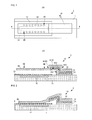
- Fig. 1(A) is a plan view of a piezoelectric actuator 1 according to this embodiment, and Fig. 1(B) is a side cross-sectional view of the same.
- Fig. 2 is a side cross-sectional view of the movable portion of the piezoelectric actuator 1 in a bent state.
- the piezoelectric actuator 1 has an insulating base substrate 11 with a predetermined area and a predetermined thickness.
- the base substrate 1 is formed with a length of 1.5 mm and a width of 0.5 mm in plan view, for example.
- a recess is formed in a predetermined region on one principal surface (top side in Fig. 1(B) ) of the base substrate 11.
- a fixed electrode 12 is formed inside the recess.
- a dielectric layer 13 is formed in a predetermined region on the surface (one principal surface) of the base substrate 11 where the fixed electrode 12 is formed, at a predetermined thickness so as to cover at least the fixed electrode 12.
- a lower electrode 14 is formed at a predetermined thickness in a predetermined region on the surface of the base substrate 11.
- the lower electrode 14 has an upright bending portion 14V in its intermediate portion, and a portion 14ED of the lower electrode 14 is separated from the base substrate 11 by a predetermined distance.
- the bending portion 14V is upright in Fig. 1(B)
- the bending portion 14V is formed into a shape inclined at a predetermined angle (e.g., 45 degrees) in a manufacturing method described later.
- the intermediate portion in which the bending portion 14V is provided may be any position in the lower electrode 14, the dimensions of the portion 14ED separated from the base substrate 11 are defined so that a predetermined piezoelectric drive is obtained.
- a piezoelectric layer 15 is formed in a predetermined region and at a predetermined thickness so as to cover the lower electrode 14. Also, the piezoelectric layer 15 has a bending portion 15V that conforms to the bending portion 14V of the lower electrode 14. At this time, the piezoelectric layer 15 is formed so as to cover even the portion 14ED of the lower electrode 14 which is separated from the base substrate 11. This structure ensures separation between the lower electrode 14 and the upper electrode 16 when an upper electrode 16 described later is formed.
- the upper electrode 16 is formed as an integrated structure of a support portion 61 and a movable portion 62. Although an end of the support portion 61 also bends as the piezoelectric layer 15 is distorted, for the convenience of explanation, the upper electrode 16 is divided into the support portion 61 and the movable 62 in the following description.
- the support portion 61 is formed in a predetermined region at a predetermine thickness so as to cover the piezoelectric layer 15.
- the upper electrode 16 has a bending portion 16V that conforms to the bending portion 14V of the lower electrode 14, and the bending portion 15V of the piezoelectric layer 15.
- the movable portion 62 connects to an end 61ED of the support portion 61 not facing the lower electrode 14. As illustrated in Fig.
- the movable portion 62 in plan view of the piezoelectric actuator 1, is formed at a predetermined thickness with an area such that the movable portion 62 faces at least the fixed electrode 12.
- the movable portion 62 has multiple through-holes 60 formed in a predetermined arrangement pattern. The provision of the through-holes 60 causes the cross-sectional area orthogonal to the longitudinal direction to differ between where the through-holes 60 exist and where the through-holes 60 do not exist. Therefore, the movable portion 62 is easily bent, effectively producing continuous or multistep variations in the movable portion 62 in a variable capacitance element described later.
- the multiple through-holes 60 may not necessarily be formed in an equidistant arrangement pattern but may be arranged in an arbitrary manner according to the bending of the movable portion 62, for example, in such a way that makes the arrangement pattern differ between the distal end side of the movable portion 62 and the side of the movable portion 62 close to the support portion 61. Since the main purpose of the through-holes 60 is to create variations in cross-sectional area, their shape may not be circular but may be elliptical or polygonal in plan view. Such holes may not be through-holes but may be semi-through holes. The through-holes 60 may not be provided as long as a desired piezoelectric drive can be attained.
- one end of the flat plate-shaped movable portion 62 of the upper electrode 16 is supported by a support column that is formed by a stacked structure of the support portion 61 of the upper electrode 16, the piezoelectric layer 15, and the lower electrode 14, so as to be separated from the surface of the base substrate 11 by a predetermined distance.
- the piezoelectric layer 15 is distorted, producing a bend in the portion from the vicinity of an end of the support column including the support portion 61 of the upper electrode 16, the piezoelectric layer 15, and the lower electrode 14 to the movable portion 62.
- the movable portion 62 of the upper electrode 16 comes into contact with the surface of the dielectric layer 13 of the base substrate 11.
- the movable portion 62 of the upper electrode 16 and the fixed electrode 12 face each other via the dielectric layer 13.
- a capacitor defined by the facing area between the movable portion 62 of the upper electrode 16 and the fixed electrode 12, and the thickness and dielectric constant of the dielectric layer 13 is formed.
- the capacitance of the capacitor ranges from 0.01 pF to 10 pF.
- a transmission line that transmits desired high frequency signals is connected to the upper electrode 16 and the fixed electrode 12.
- the movable portion 62 of the upper electrode 16 and the fixed electrode 12 are separated from each other, not conducting high frequency signals.
- a capacitor with a predetermined capacitance is formed, resulting in a high frequency conducting state. Therefore, this structure allows the piezoelectric actuator 1 to function as a high frequency switch. Also, other than being connected to a transmission line that transmits high frequency signals, the piezoelectric actuator 1 can be also connected between the transmission line and a ground line to function as a switch.
- the upper electrode 16 for applying a drive voltage is made to double as a movable electrode for high frequency signals, thus enabling a more simplified structure than the structure according to the related art in which the arm and the movable electrode are formed separately.
- the lower electrode 14, the piezoelectric layer 15, and the support portion 61 of the upper electrode 16 function as the support column for the arm, thus enabling a more simplified structure than the structure according to the related art in which the lower electrode 14, the piezoelectric layer 15, and the upper electrode 16 are provided after the arm is provided separately.
- the fixed electrode 12 is provided to the base substrate 11, thus enabling a more simplified structure than in the case of separately providing the fixed electrode 12 to a cover or the like.
- the structure according to this embodiment makes it possible to form a piezoelectric actuator by means of a structure that is simpler than in the related art.
- the piezoelectric actuator can be also used as a variable capacitance element by adjusting the drive voltage level in a continuous or multistep manner.
- distortion of the piezoelectric layer 15 can be also adjusted in a continuous or multistep manner.
- the degree of distortion of the piezoelectric layer 15 changes, the bent state also changes, and so does the area of contact of the movable portion 62 of the upper electrode 16 with the dielectric layer 13.
- a change in the contact area also causes a change in the capacitance value of the capacitor formed by the movable portion 62 of the upper electrode 16, the fixed electrode 12, and the dielectric layer 13.
- the length of the movable portion 62 in side view is longer than the length of the fixed electrode 12 in side view, and the distal end side of the movable portion 62 does not overlap the fixed electrode 12 in plan view.
- the distal end side of the movable portion 62 hangs down under its own weight while no drive voltage is applied, or when the distal end side of the movable portion 62 abruptly comes into contact with the dielectric layer 13 due to unwanted sticking upon application of a drive voltage, the distal end side of the movable portion 62 does not come to face the fixed electrode 12 via the dielectric layer 13.
- the function as a switch or the function as a variable capacitance element mentioned above can be realized more reliably.
- Fig. 3 is a flowchart illustrating a manufacturing flow of the piezoelectric actuator 1 according to the first embodiment.
- Fig. 4 is a side cross-sectional view illustrating a structure in each step of the flow illustrated in Fig. 3 .
- a recess of 500 nm to 5 ⁇ m (typically 3 ⁇ m) is formed by dry etching in the base substrate 11 made of a glass with a thickness of 100 ⁇ m to 500 ⁇ m (typically 300 ⁇ m), and the fixed electrode 12 made of Cu is formed by sputtering (S101).
- the method of forming the recess may be wet etching, sand blasting, or the like. Also, the method of forming the fixed electrode 12 may be evaporation or plating, or a combination of these methods.
- an insulating material, a piezoelectric material, or a semiconductor material such as LTCC, SOI, alumina ceramics, LiNbO 3 , LiTaO 3 , quartz crystal, Si, sapphire, GaAs, GaN, Ge, or SiC may be used.
- a metal with a high melting point or electrical conductivity such as Au, Ag, Pt, Ru, or Ir
- a stacked electrode having multiple metals stacked on one another, a Cu alloy, or an Ag alloy such as Ag-Pd may be used as
- a barrier film of TiN, TaN, TiSiN, or the like may be formed on the Cu electrode by sputtering at a thickness of about 100 nm in order to prevent oxidation and diffusion of Cu or the like.
- the dielectric layer 13 made of Ta 2 O 5 (dielectric constant: 25) is formed by patterning in a predetermined shape by dry etching, at a thickness of 100 nm to 1 ⁇ m (typically 200 nm) on the surface on the fixed electrode 12 side of the base substrate 11 (S102).
- the method of forming the dielectric layer 13 may be evaporation or plating, and the patterning may be a wet method.
- a SiN x , SiO 2 , Al 2 O 3 , (Ba, Sr) TiO system e.g., nitrogen doping
- a material with a dielectric constant of 5 to 1000, more preferably 20 to 150 may be used.
- the dielectric layer 13 may be formed as a multilayer structure by using multiple dielectric materials.
- a dummy layer 50 made of ZnO is formed by patterning in a predetermined shape by wet etching, at a thickness of 1 to 10 ⁇ m (typically 3 ⁇ m) on the surface of the dielectric layer 13 (S103).
- the method of forming the dummy layer 50 may be evaporation or plating, and the patterning may be dry etching.
- the material of the dummy layer 50 other than ZnO, polysilicon or the like may be used.
- the crystallinity of the lower electrode 14 and dielectric layer 15 that are formed in subsequent steps improves owing to orientation of the ZnO.
- the characteristics and reliability of the piezoelectric actuator 1 can be improved.
- the lower electrode 14 made of Pt is formed by patterning in a predetermined shape by dry etching, at a thickness of 100 to 500 nm (typically 200 nm) on the surfaces of the dummy layer 50 and base substrate 11 (S104).
- the method of forming the lower electrode 14 may be evaporation or plating, and the patterning may be wet etching.
- the bending portion 14V is formed in the lower electrode 14, and the portion 14ED of the lower electrode 14 separated from the base substrate 11 is formed.
- the material of the lower electrode 14 a material with a high melting point that is stable even under high temperatures is preferred.
- the material may be Ir, Ru, or an oxide thereof, a conductive oxide nitride such as LaNiO 3 , SrRuO 3 , SrIrO 3 , SrCoO 3 , LaTiO 2 N 1 , (Sr, La)TiO x N y , or a stacked structure thereof.
- a titanium oxide material is preferably used as the underlying layer.
- LaNiO 3 , SrRuO 3 , LaTiO 2 N 1 , and (Sr, La)TiO x N y for the surface layer of the lower electrode 14 improves the crystallinity of the piezoelectric layer 15 owing to orientation of those oxides. Thus, the characteristics and reliability of the piezoelectric actuator 1 can be improved.
- the method of forming the piezoelectric layer 15 may be CVD or PLD, and the patterning may be wet etching.
- the patterning is performed in such a way that the piezoelectric layer 15 covers the portion 14ED of the lower electrode 14 which is separated from the base electrode 11. This makes it possible to prevent the upper electrode 16 from coming into contact with the lower electrode 14 when the upper electrode 16 is formed in a subsequent step.
- a material of the piezoelectric layer 15 other than the above-mentioned KNN (potassium sodium niobate) system that is a non-lead piezoelectric material, a PZT (lead zirconate titanate), AIN (aluminum nitride), or ZnO (zinc oxide) material may be used.
- the characteristics of and manufacturing methods for these materials as piezoelectric thin films are already well-known, it is easy to form the piezoelectric layer 15 with stable quality.
- use of a KNN system can further improve environmental properties as well.
- annealing at 500°C to 900 such as RTA after forming the piezoelectric layer 15 (before forming the upper electrode 16), the crystallinity, reliability, and piezoelectric characteristics of the piezoelectric can be improved.
- the upper electrode 16 made of Cy is formed by patterning in a predetermined shape by dry etching, at a thickness of 500 nm to 5 ⁇ m (typically 2 ⁇ m) on the surfaces of the piezoelectric layer 15 and dummy layer 50 (S106).
- the method of forming the upper electrode 16 may be sputtering or plating, and the patterning may be wet etching.
- Au, Ag, Ni, or the like may be used other than Cu.
- the material may be an alloy system of these metals.
- the upper electrode 16 may be an Au stacked electrode or the like using a titanium oxide material as the underlying layer.
- a barrier film of TiN, TaN, TiSiN, or the like may be formed on the electrode made of Cu or the like by sputtering at a thickness of about 100 nm in order to prevent oxidation and diffusion of the Cu or the like of the upper electrode 16. Since the upper electrode 16 is formed in a step later than the formation of the piezoelectric layer 15 which is a high temperature process, a conductive material that is not affected by the deposition process temperature of the piezoelectric layer can be used for the upper electrode 16. This improves the freedom of selection for the material of the upper electrode 16 that is formed over a significantly larger area than the lower electrode 14 and the piezoelectric layer 15.
- the upper electrode 16 makes it possible to adjust the stress generated in the dummy layer 50, the lower electrode 14, and the piezoelectric layer 15 that are formed in preceding steps, by means of the film thickness of the upper electrode 16.
- the dummy layer 50 is removed by wet etching (S107).
- the speed of wet etching can be improved, thereby enabling improved tact time of the dummy layer removing step.
- the piezoelectric actuator 1 is completed through the above-mentioned steps.
- the dummy layer 50 is deposited by using a low pressure chemical vapor deposition (LPCVD) apparatus at a temperature of about 650°C. Thereafter, after forming the lower electrode 14, the piezoelectric layer 15, and the upper electrode 16, the dummy layer 50 made of polysilicon is removed by, for example, wet etching using TMAH or dry etching using SF 6 or XeF 2 .
- LPCVD low pressure chemical vapor deposition
- the upper electrode 16 may be formed by plating.
- a resist film is formed on the entire surface of this underlying electrode.
- photolithography is used to pattern a region corresponding to the upper electrode 16, and the resist film of this region is removed.
- an adhesion layer and a plating seed layer are formed on the entire surface.
- a resist film is further formed, a region corresponding to the upper electrode 16 is patterned, and the resist film of this region is removed.
- a Cu plating or Au plating layer is formed at a thickness of 1 ⁇ m to 10 ⁇ m (typically 3 ⁇ m). Thereafter, the plating seed layer and the two resist films sandwiching the plating seed layer are removed, and further, the dummy layer 50 is removed.
- the above-mentioned manufacturing flow may include a step of forming an underlying thin film (buffer layer) between the lower electrode 14 and the piezoelectric layer 15.
- the buffer layer is formed primarily for purposes such as improving the crystallinity (orientation) of the piezoelectric layer, and reducing compressive stress or tensile stress resulting from the difference in thermal expansion coefficient between the lower electrode 14 and the piezoelectric layer 15.
- the material of the buffer layer one of BaTiO 3 , SrTiO 3 , BaZrO 3 , (Ba, Sr) TiO 3 , and GdZrO 3 as an oxide with high dielectric constant, or LaNiO 3 , SrRuO 3 , LaTiO 2 N 1 , and (Sr, La)TiO x N y as a conductive nitride oxide, or a combination of these is used.
- the method of forming the buffer layer sputtering, evaporation, plating, or the like is used.
- the thickness of the buffer layer ranges from 1 to 100 nm (typically 10 nm).
- the piezoelectric layer 15 may be formed as a multilayer structure.
- a combination of the above-mentioned KNN (potassium sodium niobate) system, PZT (lead zirconate titanate) system, AIN (aluminum nitride) system, or ZnO (zinc oxide) system mentioned above, a combination of the same systems, or the like is used.
- sputtering, evaporation, plating, or a combination of these methods is used as the method of forming the multilayer structure.
- the above-mentioned manufacturing flow may include a step of forming an intermediate layer made of an insulator material or another material between the base substrate and the lower electrode, the lower electrode and the piezoelectric layer, or the piezoelectric layer and the upper electrode.
- a piezoelectric actuator according to a second embodiment is described with reference to a drawing.
- Fig. 5 is a side cross-sectional view of a piezoelectric actuator 1A according to this embodiment.
- the piezoelectric actuator 1A according to this embodiment differs in the shape of an upper electrode 16A, and is otherwise the same. Therefore, only the structure of the upper electrode 16A is described.
- a support portion 61A and a movable portion 62A are formed of different materials.
- one end of the movable portion 62A is formed so as to cover and overlap the support portion 61A.
- This configuration also makes it possible to attain an operational effect similar to that of the first embodiment, and obtain freedom of design, such as selecting a material that provides excellent adhesion with the piezoelectric layer 15 for the support portion 61A (e.g., Pt), and selecting a material that has excellent electrical conductivity and is inexpensive (such as Cu) for the movable portion 62A.
- a piezoelectric actuator according to a third embodiment is described with reference to a drawing.
- Fig. 6 is a side cross-sectional view of a piezoelectric actuator 1B according to this embodiment.
- the piezoelectric actuator 1B according to this embodiment differs in the shapes of a lower electrode 14B, piezoelectric layer 15B, and upper electrode 16B, and is otherwise the same. Therefore, only the structures of the lower electrode 14B, piezoelectric layer 15B, and upper electrode 16B are described.
- the lower electrode 14B and the piezoelectric layer 15B are formed in such a way that an end of the lower electrode 14B protrudes beyond an end of the piezoelectric layer 15B.
- the upper electrode 16B has only a support portion 61B that is formed only on the surface of the piezoelectric layer 15.
- a movable portion 63B is formed so as to connect to the lower electrode 14B. While in the configuration illustrated in Fig.
- the movable portion 63B is formed at such a thickness that the movable portion 63B does not contact the upper electrode 16B, freedom in the thickness of the movable portion 63B is obtained as long as contact between the upper electrode 16B and the movable portion 63B is avoided by, for example, making an end of the piezoelectric layer 15B protrude beyond an end of the upper electrode 16B. While the movable portion 63B may be formed at any timing after formation of the lower electrode 14B, forming the movable portion 63B after formation of the piezoelectric layer 15 can improve freedom in material selection without having to consider the influence of the formation process temperature of the piezoelectric layer 15 as mentioned above.
- a piezoelectric actuator according to a fourth embodiment is described with reference to a drawing.
- Fig. 7 is a side cross-sectional view of a piezoelectric actuator 1C according to this embodiment.
- the piezoelectric actuator 1C according to this embodiment differs in the position where a fixed electrode 12C is formed, and is otherwise the same. Therefore, only the structure of the fixed electrode 12C is described.
- the fixed electrode 12C is formed on the surface of the base substrate 11 having a flat shape.
- a dielectric layer 13C is formed by patterning in a shape that covers even the fixed electrode 12C. This configuration also makes it possible to attain an operational effect similar to that of the first embodiment.
- Fig. 8 is a side cross-sectional view of a piezoelectric actuator 1D according to this embodiment.
- the piezoelectric actuator 1D according to this embodiment is of substantially the same structure as the piezoelectric actuator 1 according to the first embodiment. While in Fig. 8 a fixed electrode 12D is formed to have a small area so that the fixed electrode 12D only includes a portion that faces the distal end of the movable portion 62 at a predetermined distance, the fixed electrode 12D may be of the same structure as the fixed electrode 12 according to the first embodiment.
- the structure of the piezoelectric actuator 1D is such that, by controlling a drive voltage, the movable portion 62 of the upper electrode 16 is always separated from the fixed electrode 12D and the dielectric layer 13 with a space gap Gon corresponding to the drive voltage. This structure also makes it possible to attain an operational effect similar to that of the first embodiment.
- a piezoelectric actuator according to a sixth embodiment is described with reference to a drawing.
- Fig. 9 is a side cross-sectional view of a piezoelectric actuator 1E according to this embodiment.
- the piezoelectric actuator 1E according to this embodiment differs in the structure of a dielectric layer 13E, and is otherwise the same. Therefore, only the structure of the fixed electrode 12C is described.
- the dielectric layer 13B is formed so as to be in contact with a portion of the lower electrode 14 separated from the base substrate 11, an end of the piezoelectric layer 15, and the movable portion 62 of the upper electrode 16, that is, the dielectric layer 13B is formed not on the base substrate side but on the movable portion side.
- the dielectric layer 13B can reinforce the movable portion 62. This structure also makes it possible to attain an operational effect similar to that of the first embodiment.
- a piezoelectric actuator according to a seventh embodiment is described with reference to a drawing.
- Fig. 10 is a side cross-sectional view of a piezoelectric actuator 1F according to this embodiment.
- the piezoelectric actuator 1F according to this embodiment differs in the structure of a piezoelectric layer 15F.
- the piezoelectric layer 15F of the piezoelectric actuator 1F is formed so as to be longer than the fixed electrode 12 in side view.
- the upper electrode 16 also serving as the movable portion 62 is formed on substantially the entire surface of the piezoelectric layer 15F. This configuration makes it possible for the piezoelectric layer 15F to double as the dielectric layer 13 mentioned above, thereby making it possible to omit the dielectric layer. Thus, it is possible to form a piezoelectric actuator with an even simpler configuration.
- a piezoelectric actuator according to an eighth embodiment is described with reference to a drawing.
- Fig. 11 is a side cross-sectional view of a piezoelectric actuator 1G according to this embodiment.
- the piezoelectric actuator 1G according to this embodiment differs in the structure of an upper electrode 16G.
- an insulator layer 64 is formed between a support portion 61G and a movable portion 62G. This configuration enables electrical isolation between the support portion 61G and the movable portion 62G.
- the material of the insulator layer 64 not only an insulator material such as glass or ceramics, but also the above-mentioned dielectric material, piezoelectric material, semiconductor material, or the like can be also used.
- the support portion 61G for application of a drive voltage, and use the movable portion 62 for transmission of high frequency signals.
Landscapes
- Engineering & Computer Science (AREA)
- Chemical & Material Sciences (AREA)
- Manufacturing & Machinery (AREA)
- Materials Engineering (AREA)
- Ceramic Engineering (AREA)
- General Electrical Machinery Utilizing Piezoelectricity, Electrostriction Or Magnetostriction (AREA)
- Micromachines (AREA)
Applications Claiming Priority (2)
| Application Number | Priority Date | Filing Date | Title |
|---|---|---|---|
| JP2010099778 | 2010-04-23 | ||
| PCT/JP2011/058697 WO2011132532A1 (fr) | 2010-04-23 | 2011-04-06 | Actionneur piézo-électrique et son procédé de fabrication |
Publications (2)
| Publication Number | Publication Date |
|---|---|
| EP2562836A1 true EP2562836A1 (fr) | 2013-02-27 |
| EP2562836A4 EP2562836A4 (fr) | 2014-07-23 |
Family
ID=44834063
Family Applications (1)
| Application Number | Title | Priority Date | Filing Date |
|---|---|---|---|
| EP11771868.4A Withdrawn EP2562836A4 (fr) | 2010-04-23 | 2011-04-06 | Actionneur piézo-électrique et son procédé de fabrication |
Country Status (5)
| Country | Link |
|---|---|
| US (1) | US8890392B2 (fr) |
| EP (1) | EP2562836A4 (fr) |
| JP (1) | JPWO2011132532A1 (fr) |
| CN (1) | CN102859734B (fr) |
| WO (1) | WO2011132532A1 (fr) |
Cited By (3)
| Publication number | Priority date | Publication date | Assignee | Title |
|---|---|---|---|---|
| JP2014112675A (ja) * | 2012-11-28 | 2014-06-19 | Tdk Corp | 薄膜圧電素子、薄膜圧電アクチュエータ、及び薄膜圧電センサ、並びにハードディスクドライブ、及びインクジェットプリンタ装置 |
| WO2015171224A1 (fr) * | 2014-05-09 | 2015-11-12 | Chirp Microsystems, Inc. | Transducteur à ultrasons micro-usiné utilisant de multiples matériaux piézoélectriques |
| JPWO2014007015A1 (ja) * | 2012-07-02 | 2016-06-02 | 株式会社村田製作所 | 圧電薄膜素子及びその製造方法 |
Families Citing this family (20)
| Publication number | Priority date | Publication date | Assignee | Title |
|---|---|---|---|---|
| JP2013016776A (ja) * | 2011-06-06 | 2013-01-24 | Hitachi Cable Ltd | 圧電膜素子の製造方法、及び圧電体デバイスの製造方法 |
| JP5774399B2 (ja) * | 2011-07-15 | 2015-09-09 | 株式会社サイオクス | 圧電体膜素子の製造方法 |
| KR102005335B1 (ko) * | 2011-09-02 | 2019-07-30 | 카벤디시 키네틱스, 인크. | 향상된 rf 성능의 mems 가변 커패시터 |
| JP5897436B2 (ja) * | 2012-09-13 | 2016-03-30 | 住友化学株式会社 | 圧電体薄膜付き基板の製造方法、及び圧電体薄膜素子の製造方法 |
| JP2014060267A (ja) * | 2012-09-18 | 2014-04-03 | Hitachi Metals Ltd | 圧電膜素子及びそれを備えた圧電膜デバイス |
| WO2014069061A1 (fr) * | 2012-10-31 | 2014-05-08 | 株式会社村田製作所 | Ligne de signal haute fréquence et procédé de fabrication pour celle-ci |
| WO2014083195A1 (fr) * | 2012-11-30 | 2014-06-05 | Universiteit Gent | Film mince associé à la pérovskite à orientation préférentielle |
| US9058868B2 (en) | 2012-12-19 | 2015-06-16 | International Business Machines Corporation | Piezoelectronic memory |
| US9941472B2 (en) | 2014-03-10 | 2018-04-10 | International Business Machines Corporation | Piezoelectronic device with novel force amplification |
| US9251884B2 (en) | 2014-03-24 | 2016-02-02 | International Business Machines Corporation | Non-volatile, piezoelectronic memory based on piezoresistive strain produced by piezoelectric remanence |
| JP2016001662A (ja) * | 2014-06-11 | 2016-01-07 | パナソニック株式会社 | 誘電体素子および圧電体素子 |
| US9472368B2 (en) | 2014-10-31 | 2016-10-18 | International Business Machines Corporation | Piezoelectronic switch device for RF applications |
| KR101703608B1 (ko) * | 2015-08-28 | 2017-02-07 | 현대자동차 주식회사 | 탈착형 마이크로폰 및 그 제조 방법 |
| US10594029B2 (en) * | 2016-09-30 | 2020-03-17 | Intel Corporation | Actuatable and adaptable metamaterials integrated in package |
| JP6790749B2 (ja) * | 2016-11-16 | 2020-11-25 | セイコーエプソン株式会社 | 圧電素子及び圧電素子応用デバイス |
| US10439581B2 (en) * | 2017-03-24 | 2019-10-08 | Zhuhai Crystal Resonance Technologies Co., Ltd. | Method for fabricating RF resonators and filters |
| CN109427955B (zh) * | 2017-08-31 | 2023-04-25 | 北京纳米能源与系统研究所 | 自驱动多级传感器及其制备方法、传感方法及电子皮肤 |
| US12528308B2 (en) * | 2020-05-01 | 2026-01-20 | X-Celeprint Limited | Hybrid documents with electronic indicia |
| US12437174B2 (en) | 2020-05-01 | 2025-10-07 | X-Celeprint Limited | Hybrid documents with electronic indicia |
| US12414471B2 (en) | 2020-05-01 | 2025-09-09 | X-Celeprint Limited | Piezoelectric power components |
Family Cites Families (30)
| Publication number | Priority date | Publication date | Assignee | Title |
|---|---|---|---|---|
| JP3148946B2 (ja) * | 1991-05-30 | 2001-03-26 | キヤノン株式会社 | 探針駆動機構並びに該機構を用いたトンネル電流検出装置、情報処理装置、圧電式アクチュエータ |
| DE4305033A1 (de) * | 1992-02-21 | 1993-10-28 | Siemens Ag | Mikromechanisches Relais mit Hybridantrieb |
| JP3203433B2 (ja) * | 1992-02-21 | 2001-08-27 | キヤノン株式会社 | 変位素子、及びこれを用いた検出素子、及びこの検出素子を用いた走査型トンネル顕微鏡、情報処理装置 |
| EP1724750B1 (fr) * | 1999-01-29 | 2008-08-27 | Seiko Epson Corporation | Transducteur piézoélectrique et dispositif d'affichage avec de l'encre électrophorétique utilisant le transducteur piézoélectrique |
| US6688729B1 (en) * | 1999-06-04 | 2004-02-10 | Canon Kabushiki Kaisha | Liquid discharge head substrate, liquid discharge head, liquid discharge apparatus having these elements, manufacturing method of liquid discharge head, and driving method of the same |
| US6359374B1 (en) * | 1999-11-23 | 2002-03-19 | Mcnc | Miniature electrical relays using a piezoelectric thin film as an actuating element |
| US7098577B2 (en) * | 2002-10-21 | 2006-08-29 | Hrl Laboratories, Llc | Piezoelectric switch for tunable electronic components |
| EP1457471B1 (fr) | 2003-03-14 | 2014-02-26 | Denso Corporation | Céramiques à orientation cristalline et procédés pour leur préparation |
| JP4053958B2 (ja) * | 2003-09-19 | 2008-02-27 | 株式会社東芝 | 電圧制御発振器 |
| EP1726048B1 (fr) * | 2003-12-22 | 2008-09-10 | Nxp B.V. | Composant electronique |
| US7323805B2 (en) * | 2004-01-28 | 2008-01-29 | Kabushiki Kaisha Toshiba | Piezoelectric thin film device and method for manufacturing the same |
| JP4408266B2 (ja) * | 2004-04-22 | 2010-02-03 | 日本碍子株式会社 | マイクロスイッチ及びその製造方法 |
| JP4707667B2 (ja) * | 2004-09-01 | 2011-06-22 | 株式会社アドバンテスト | バイモルフ素子、バイモルフスイッチ、ミラー素子及びこれらの製造方法 |
| JP4580745B2 (ja) * | 2004-12-08 | 2010-11-17 | 株式会社東芝 | 圧電駆動型mems装置 |
| JP4580826B2 (ja) * | 2005-06-17 | 2010-11-17 | 株式会社東芝 | マイクロメカニカルデバイス、マイクロスイッチ、容量可変キャパシタ、高周波回路及び光学スイッチ |
| JP4713990B2 (ja) * | 2005-09-13 | 2011-06-29 | 株式会社東芝 | 半導体装置とその製造方法 |
| JP4834443B2 (ja) | 2006-03-31 | 2011-12-14 | 株式会社東芝 | 圧電駆動型memsアクチュエータ |
| US7479726B2 (en) * | 2006-04-06 | 2009-01-20 | Kabushiki Kaisha Toshiba | MEMS device using an actuator |
| US7586238B2 (en) * | 2006-08-17 | 2009-09-08 | Freescale Semiconductor, Inc. | Control and testing of a micro electromechanical switch having a piezo element |
| JP4220541B2 (ja) * | 2006-09-22 | 2009-02-04 | 株式会社東芝 | Mems装置 |
| JP4328981B2 (ja) * | 2007-01-25 | 2009-09-09 | セイコーエプソン株式会社 | 圧電振動子の製造方法 |
| JP2008238330A (ja) | 2007-03-27 | 2008-10-09 | Toshiba Corp | Mems装置およびこのmems装置を有する携帯通信端末 |
| JP2008258186A (ja) * | 2007-03-30 | 2008-10-23 | Matsushita Electric Ind Co Ltd | 可変容量デバイス |
| DE102007024901A1 (de) * | 2007-05-29 | 2008-12-11 | Siemens Ag | Kondensatorstruktur mit veränderbarer Kapzität und Verwendung der Kondensatorstruktur |
| JP2009055683A (ja) * | 2007-08-24 | 2009-03-12 | Toshiba Corp | 圧電駆動型mems装置および携帯端末 |
| JP5227566B2 (ja) * | 2007-11-06 | 2013-07-03 | 株式会社東芝 | アクチュエータ |
| US8274200B2 (en) * | 2007-11-19 | 2012-09-25 | Xcom Wireless, Inc. | Microfabricated cantilever slider with asymmetric spring constant |
| JP2009238546A (ja) | 2008-03-26 | 2009-10-15 | Panasonic Electric Works Co Ltd | 微小電気機械スイッチ |
| JP2009256147A (ja) * | 2008-04-18 | 2009-11-05 | Denso Corp | 異方形状粉末及び結晶配向セラミックスの製造方法 |
| JP5300559B2 (ja) * | 2009-03-30 | 2013-09-25 | 株式会社東芝 | 圧電駆動型mems素子 |
-
2011
- 2011-04-06 EP EP11771868.4A patent/EP2562836A4/fr not_active Withdrawn
- 2011-04-06 CN CN201180019897.7A patent/CN102859734B/zh active Active
- 2011-04-06 WO PCT/JP2011/058697 patent/WO2011132532A1/fr not_active Ceased
- 2011-04-06 JP JP2012511604A patent/JPWO2011132532A1/ja active Pending
-
2012
- 2012-10-22 US US13/656,800 patent/US8890392B2/en active Active
Cited By (5)
| Publication number | Priority date | Publication date | Assignee | Title |
|---|---|---|---|---|
| JPWO2014007015A1 (ja) * | 2012-07-02 | 2016-06-02 | 株式会社村田製作所 | 圧電薄膜素子及びその製造方法 |
| JP2014112675A (ja) * | 2012-11-28 | 2014-06-19 | Tdk Corp | 薄膜圧電素子、薄膜圧電アクチュエータ、及び薄膜圧電センサ、並びにハードディスクドライブ、及びインクジェットプリンタ装置 |
| WO2015171224A1 (fr) * | 2014-05-09 | 2015-11-12 | Chirp Microsystems, Inc. | Transducteur à ultrasons micro-usiné utilisant de multiples matériaux piézoélectriques |
| US10566949B2 (en) | 2014-05-09 | 2020-02-18 | Chirp Microsystems, Inc. | Micromachined ultrasound transducer using multiple piezoelectric materials |
| US11711067B2 (en) | 2014-05-09 | 2023-07-25 | Invensense, Inc. | Micromachined ultrasound transducer using multiple piezoelectric materials |
Also Published As
| Publication number | Publication date |
|---|---|
| WO2011132532A1 (fr) | 2011-10-27 |
| US20130043767A1 (en) | 2013-02-21 |
| US8890392B2 (en) | 2014-11-18 |
| EP2562836A4 (fr) | 2014-07-23 |
| CN102859734B (zh) | 2014-12-10 |
| JPWO2011132532A1 (ja) | 2013-07-18 |
| CN102859734A (zh) | 2013-01-02 |
Similar Documents
| Publication | Publication Date | Title |
|---|---|---|
| US8890392B2 (en) | Piezoelectric actuator having a moveable electrode portion | |
| CN100544049C (zh) | 压电驱动mems器件 | |
| US7459827B2 (en) | Piezoelectric-driven MEMS device and method for manufacturing the same | |
| US7459833B2 (en) | Thin film piezoelectric actuator | |
| KR101092536B1 (ko) | 압전형 rf 멤스 소자 및 그 제조방법 | |
| CN101373811B (zh) | 压电驱动型mems装置及便携终端 | |
| US20030179535A1 (en) | Tunable capacitor and method of fabricating the same | |
| US20130140156A1 (en) | Piezoelectric actuator and method for manufacturing same | |
| US7728703B2 (en) | RF MEMS switch and method for fabricating the same | |
| EP1726048B1 (fr) | Composant electronique | |
| US7479726B2 (en) | MEMS device using an actuator | |
| US7960900B2 (en) | Assembly of a microswitch and of an acoustic resonator | |
| JP4504237B2 (ja) | ウエットエッチング方法、マイクロ可動素子製造方法、およびマイクロ可動素子 | |
| US20080047816A1 (en) | Mems switch | |
| US7952259B2 (en) | Electronic apparatus with a micro-electromechanical switch made of a piezoeletric material | |
| US7939993B2 (en) | Micromechanical Hf switching element and method for the production thereof | |
| JP2007296625A (ja) | Mems | |
| JP2014229403A (ja) | スイッチ及びスイッチ装置及びスイッチ装置の駆動方法 |
Legal Events
| Date | Code | Title | Description |
|---|---|---|---|
| PUAI | Public reference made under article 153(3) epc to a published international application that has entered the european phase |
Free format text: ORIGINAL CODE: 0009012 |
|
| 17P | Request for examination filed |
Effective date: 20120820 |
|
| AK | Designated contracting states |
Kind code of ref document: A1 Designated state(s): AL AT BE BG CH CY CZ DE DK EE ES FI FR GB GR HR HU IE IS IT LI LT LU LV MC MK MT NL NO PL PT RO RS SE SI SK SM TR |
|
| DAX | Request for extension of the european patent (deleted) | ||
| A4 | Supplementary search report drawn up and despatched |
Effective date: 20140623 |
|
| RIC1 | Information provided on ipc code assigned before grant |
Ipc: B81B 3/00 20060101ALI20140616BHEP Ipc: H02N 2/00 20060101ALI20140616BHEP Ipc: H01L 41/22 20130101ALI20140616BHEP Ipc: H01L 41/09 20060101AFI20140616BHEP Ipc: H01L 41/18 20060101ALI20140616BHEP Ipc: H01H 57/00 20060101ALI20140616BHEP Ipc: B81C 1/00 20060101ALI20140616BHEP |
|
| 17Q | First examination report despatched |
Effective date: 20150902 |
|
| STAA | Information on the status of an ep patent application or granted ep patent |
Free format text: STATUS: EXAMINATION IS IN PROGRESS |
|
| GRAP | Despatch of communication of intention to grant a patent |
Free format text: ORIGINAL CODE: EPIDOSNIGR1 |
|
| STAA | Information on the status of an ep patent application or granted ep patent |
Free format text: STATUS: GRANT OF PATENT IS INTENDED |
|
| RIC1 | Information provided on ipc code assigned before grant |
Ipc: H01L 41/316 20130101ALI20170428BHEP Ipc: H01L 41/09 20060101AFI20170428BHEP Ipc: H01L 41/331 20130101ALI20170428BHEP |
|
| INTG | Intention to grant announced |
Effective date: 20170529 |
|
| RIN1 | Information on inventor provided before grant (corrected) |
Inventor name: YAMAMOTO, KANSHO Inventor name: YAMAMOTO, TEIJI Inventor name: KOUTSAROFF, P. IVO |
|
| STAA | Information on the status of an ep patent application or granted ep patent |
Free format text: STATUS: THE APPLICATION IS DEEMED TO BE WITHDRAWN |
|
| 18D | Application deemed to be withdrawn |
Effective date: 20171010 |