EP2562837A1 - Dispositif ferroélectrique - Google Patents
Dispositif ferroélectrique Download PDFInfo
- Publication number
- EP2562837A1 EP2562837A1 EP11771971A EP11771971A EP2562837A1 EP 2562837 A1 EP2562837 A1 EP 2562837A1 EP 11771971 A EP11771971 A EP 11771971A EP 11771971 A EP11771971 A EP 11771971A EP 2562837 A1 EP2562837 A1 EP 2562837A1
- Authority
- EP
- European Patent Office
- Prior art keywords
- ferroelectric
- shock absorbing
- absorbing layer
- silicon substrate
- film
- Prior art date
- Legal status (The legal status is an assumption and is not a legal conclusion. Google has not performed a legal analysis and makes no representation as to the accuracy of the status listed.)
- Withdrawn
Links
Images

Classifications
-
- G—PHYSICS
- G01—MEASURING; TESTING
- G01J—MEASUREMENT OF INTENSITY, VELOCITY, SPECTRAL CONTENT, POLARISATION, PHASE OR PULSE CHARACTERISTICS OF INFRARED, VISIBLE OR ULTRAVIOLET LIGHT; COLORIMETRY; RADIATION PYROMETRY
- G01J1/00—Photometry, e.g. photographic exposure meter
- G01J1/02—Details
-
- B—PERFORMING OPERATIONS; TRANSPORTING
- B81—MICROSTRUCTURAL TECHNOLOGY
- B81C—PROCESSES OR APPARATUS SPECIALLY ADAPTED FOR THE MANUFACTURE OR TREATMENT OF MICROSTRUCTURAL DEVICES OR SYSTEMS
- B81C1/00—Manufacture or treatment of devices or systems in or on a substrate
- B81C1/00642—Manufacture or treatment of devices or systems in or on a substrate for improving the physical properties of a device
- B81C1/0065—Mechanical properties
- B81C1/00658—Treatments for improving the stiffness of a vibrating element
-
- G—PHYSICS
- G01—MEASURING; TESTING
- G01J—MEASUREMENT OF INTENSITY, VELOCITY, SPECTRAL CONTENT, POLARISATION, PHASE OR PULSE CHARACTERISTICS OF INFRARED, VISIBLE OR ULTRAVIOLET LIGHT; COLORIMETRY; RADIATION PYROMETRY
- G01J5/00—Radiation pyrometry, e.g. infrared or optical thermometry
- G01J5/02—Constructional details
- G01J5/04—Casings
-
- G—PHYSICS
- G01—MEASURING; TESTING
- G01J—MEASUREMENT OF INTENSITY, VELOCITY, SPECTRAL CONTENT, POLARISATION, PHASE OR PULSE CHARACTERISTICS OF INFRARED, VISIBLE OR ULTRAVIOLET LIGHT; COLORIMETRY; RADIATION PYROMETRY
- G01J5/00—Radiation pyrometry, e.g. infrared or optical thermometry
- G01J5/02—Constructional details
- G01J5/04—Casings
- G01J5/046—Materials; Selection of thermal materials
-
- G—PHYSICS
- G01—MEASURING; TESTING
- G01J—MEASUREMENT OF INTENSITY, VELOCITY, SPECTRAL CONTENT, POLARISATION, PHASE OR PULSE CHARACTERISTICS OF INFRARED, VISIBLE OR ULTRAVIOLET LIGHT; COLORIMETRY; RADIATION PYROMETRY
- G01J5/00—Radiation pyrometry, e.g. infrared or optical thermometry
- G01J5/10—Radiation pyrometry, e.g. infrared or optical thermometry using electric radiation detectors
- G01J5/34—Radiation pyrometry, e.g. infrared or optical thermometry using electric radiation detectors using capacitors, e.g. pyroelectric capacitors
-
- G—PHYSICS
- G01—MEASURING; TESTING
- G01P—MEASURING LINEAR OR ANGULAR SPEED, ACCELERATION, DECELERATION, OR SHOCK; INDICATING PRESENCE, ABSENCE, OR DIRECTION, OF MOVEMENT
- G01P15/00—Measuring acceleration; Measuring deceleration; Measuring shock, i.e. sudden change of acceleration
- G01P15/02—Measuring acceleration; Measuring deceleration; Measuring shock, i.e. sudden change of acceleration by making use of inertia forces using solid seismic masses
- G01P15/08—Measuring acceleration; Measuring deceleration; Measuring shock, i.e. sudden change of acceleration by making use of inertia forces using solid seismic masses with conversion into electric or magnetic values
- G01P15/09—Measuring acceleration; Measuring deceleration; Measuring shock, i.e. sudden change of acceleration by making use of inertia forces using solid seismic masses with conversion into electric or magnetic values by piezoelectric pick-up
-
- H—ELECTRICITY
- H02—GENERATION; CONVERSION OR DISTRIBUTION OF ELECTRIC POWER
- H02N—ELECTRIC MACHINES NOT OTHERWISE PROVIDED FOR
- H02N2/00—Electric machines in general using piezoelectric effect, electrostriction or magnetostriction
- H02N2/18—Electric machines in general using piezoelectric effect, electrostriction or magnetostriction producing electrical output from mechanical input, e.g. generators
- H02N2/186—Vibration harvesters
-
- H—ELECTRICITY
- H10—SEMICONDUCTOR DEVICES; ELECTRIC SOLID-STATE DEVICES NOT OTHERWISE PROVIDED FOR
- H10N—ELECTRIC SOLID-STATE DEVICES NOT OTHERWISE PROVIDED FOR
- H10N15/00—Thermoelectric devices without a junction of dissimilar materials; Thermomagnetic devices, e.g. using the Nernst-Ettingshausen effect
- H10N15/10—Thermoelectric devices using thermal change of the dielectric constant, e.g. working above and below the Curie point
-
- H—ELECTRICITY
- H10—SEMICONDUCTOR DEVICES; ELECTRIC SOLID-STATE DEVICES NOT OTHERWISE PROVIDED FOR
- H10N—ELECTRIC SOLID-STATE DEVICES NOT OTHERWISE PROVIDED FOR
- H10N30/00—Piezoelectric or electrostrictive devices
- H10N30/30—Piezoelectric or electrostrictive devices with mechanical input and electrical output, e.g. functioning as generators or sensors
-
- H—ELECTRICITY
- H10—SEMICONDUCTOR DEVICES; ELECTRIC SOLID-STATE DEVICES NOT OTHERWISE PROVIDED FOR
- H10N—ELECTRIC SOLID-STATE DEVICES NOT OTHERWISE PROVIDED FOR
- H10N30/00—Piezoelectric or electrostrictive devices
- H10N30/30—Piezoelectric or electrostrictive devices with mechanical input and electrical output, e.g. functioning as generators or sensors
- H10N30/304—Beam type
- H10N30/306—Cantilevers
-
- H—ELECTRICITY
- H10—SEMICONDUCTOR DEVICES; ELECTRIC SOLID-STATE DEVICES NOT OTHERWISE PROVIDED FOR
- H10N—ELECTRIC SOLID-STATE DEVICES NOT OTHERWISE PROVIDED FOR
- H10N30/00—Piezoelectric or electrostrictive devices
- H10N30/704—Piezoelectric or electrostrictive devices based on piezoelectric or electrostrictive films or coatings
- H10N30/706—Piezoelectric or electrostrictive devices based on piezoelectric or electrostrictive films or coatings characterised by the underlying bases, e.g. substrates
- H10N30/708—Intermediate layers, e.g. barrier, adhesion or growth control buffer layers
-
- B—PERFORMING OPERATIONS; TRANSPORTING
- B81—MICROSTRUCTURAL TECHNOLOGY
- B81B—MICROSTRUCTURAL DEVICES OR SYSTEMS, e.g. MICROMECHANICAL DEVICES
- B81B2201/00—Specific applications of microelectromechanical systems
- B81B2201/03—Microengines and actuators
- B81B2201/032—Bimorph and unimorph actuators, e.g. piezo and thermo
-
- G—PHYSICS
- G01—MEASURING; TESTING
- G01P—MEASURING LINEAR OR ANGULAR SPEED, ACCELERATION, DECELERATION, OR SHOCK; INDICATING PRESENCE, ABSENCE, OR DIRECTION, OF MOVEMENT
- G01P15/00—Measuring acceleration; Measuring deceleration; Measuring shock, i.e. sudden change of acceleration
- G01P15/02—Measuring acceleration; Measuring deceleration; Measuring shock, i.e. sudden change of acceleration by making use of inertia forces using solid seismic masses
- G01P15/08—Measuring acceleration; Measuring deceleration; Measuring shock, i.e. sudden change of acceleration by making use of inertia forces using solid seismic masses with conversion into electric or magnetic values
- G01P2015/0805—Measuring acceleration; Measuring deceleration; Measuring shock, i.e. sudden change of acceleration by making use of inertia forces using solid seismic masses with conversion into electric or magnetic values being provided with a particular type of spring-mass-system for defining the displacement of a seismic mass due to an external acceleration
- G01P2015/0822—Measuring acceleration; Measuring deceleration; Measuring shock, i.e. sudden change of acceleration by making use of inertia forces using solid seismic masses with conversion into electric or magnetic values being provided with a particular type of spring-mass-system for defining the displacement of a seismic mass due to an external acceleration for defining out-of-plane movement of the mass
- G01P2015/0825—Measuring acceleration; Measuring deceleration; Measuring shock, i.e. sudden change of acceleration by making use of inertia forces using solid seismic masses with conversion into electric or magnetic values being provided with a particular type of spring-mass-system for defining the displacement of a seismic mass due to an external acceleration for defining out-of-plane movement of the mass for one single degree of freedom of movement of the mass
- G01P2015/0828—Measuring acceleration; Measuring deceleration; Measuring shock, i.e. sudden change of acceleration by making use of inertia forces using solid seismic masses with conversion into electric or magnetic values being provided with a particular type of spring-mass-system for defining the displacement of a seismic mass due to an external acceleration for defining out-of-plane movement of the mass for one single degree of freedom of movement of the mass the mass being of the paddle type being suspended at one of its longitudinal ends
Definitions
- the invention relates generally to ferroelectric devices and, more particularly, to a ferroelectric device that uses a piezoelectric effect or a pyroelectric effect of a ferroelectric film.
- ferroelectric devices that use a piezoelectric effect or a pyroelectric effect of a ferroelectric film have been attracting attention.
- a MEMS (micro electro mechanical systems) device that comprises a functional portion having a ferroelectric film in one surface side of a silicon substrate, has been proposed, from the viewpoint of the cost reduction, the mechanical strength and the like.
- a MEMS device of this type for example, a power generating device (for example, see R.
- ferroelectric material that exhibits both of the piezoelectric effect and the pyroelectric effect
- PZT(:Pb(Zr,Ti)03) or the like that is a type of a lead-based oxide ferroelectric has been known widely.
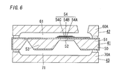
- the power generating device disclosed in the document of R. van Schaijk comprises a main unit 41 formed by using a silicon substrate 50.
- the main unit 41 comprises a frame portion 51, a cantilever (a beam) 52 that is disposed within the frame portion 51 and is swingably supported by the frame portion 51, and a weight portion 53 that is disposed at a tip of the cantilever 52.
- a functional portion 54 which comprises a power generating portion for generating AC voltage in response to the swing of the cantilever 52, is provided in the cantilever 52 of the main unit 41.
- the functional portion 54 comprises a lower electrode 54A formed of a Pt film, a ferroelectric film (a piezoelectric membrane) 54B that is formed of an AIN thin film or a PZT thin film and is provided on one surface side of the lower electrode 54A opposite to the cantilever 52 side, and an upper electrode 54C that is formed of an Al film and is provided on one surface side of the ferroelectric film 54B opposite to the lower electrode 54A side.
- a lower electrode 54A formed of a Pt film
- a ferroelectric film (a piezoelectric membrane) 54B that is formed of an AIN thin film or a PZT thin film and is provided on one surface side of the lower electrode 54A opposite to the cantilever 52 side
- an upper electrode 54C that is formed of an Al film and is provided on one surface side of the ferroelectric film 54B opposite to the lower electrode 54A side.
- the power generating device comprises a first cover substrate 42 that is formed by using a first glass substrate 60A and a second cover substrate 43 that is formed by using a second glass substrate 70A. Then, in one surface side (an upper side in Fig. 6 ) of the main unit 41, the frame portion 51 is fixed to the first cover substrate 42. Then, in the other surface side (a lower side in Fig. 6 ) of the main unit 41, the frame portion 51 is fixed to the second cover substrate 43.
- a displacement space 61 is provided between the first cover substrates 42 and a movable portion consisting of the cantilever 52 and the weight portion 53 in the main unit 41, and likewise a displacement space 71 is provided between the second cover substrates 43 and the movable portion, and thereby the movable portion can be displaced.
- the functional portion 54 that comprises the lower electrode 54A, the ferroelectric film 54B and the upper electrode 54C is formed, by using a reactive sputter method or the like, on said one surface side of the silicon substrate 50.
- a PZT thin film formed by using various thin film formation technologies, such as a sputter method or the like, on one surface side of a silicon substrate has polycrystal.
- such a PZT thin film has poor quality of crystallinity and also has small piezoelectric constant e 31 , compared with a monocrystal PZT thin film formed on one surface side of a monocrystal MgO substrate or on one surface side of a monocrystal SrTiO3 substrate being more extremely-expensive than the silicon substrate.
- various methods for forming a PZT thin film having good crystallinity on one surface side of a monocrystal silicon substrate have been researched and developed at various facilities.
- the reality is that a PZT thin film having sufficient crystallinity has not yet been obtained.
- a ferroelectric device such as a power generating device, a pyroelectric infrared sensor or the like, that comprises a functional portion having a ferroelectric film on one surface side of a silicon substrate
- a buffer layer is provided between a lower electrode and the ferroelectric film for improving the characteristic.
- a functional portion that comprises a lower electrode, a ferroelectric film and an upper electrode is formed on one surface side of a silicon substrate and then a region of the silicon substrate corresponding to the functional portion is etched from the other surface side of the silicon substrate to a predetermined depth, thereby forming a cavity in the silicon substrate and manufacturing a ferroelectric device
- the ferroelectric device is a pyroelectric infrared sensor, the device property (the response speed or the like) is reduced due to heat capacity of the thin portion.
- a ferroelectric device of the present invention comprises: a silicon substrate; a first electrode formed on one surface side of said silicon substrate; a ferroelectric film formed on a surface of said first electrode opposite to said silicon substrate side; and a second electrode formed on a surface of said ferroelectric film opposite to said first electrode side, wherein said ferroelectric film is formed of a ferroelectric material with a lattice constant difference from silicon, wherein the ferroelectric device further comprises a shock absorbing layer, said shock absorbing layer being formed of a material with better lattice matching with said ferroelectric film than silicon and being provided between said silicon substrate and said first electrode, wherein said silicon substrate is provided with a cavity that exposes a surface of said shock absorbing layer opposite to said first electrode side.
- the crystallinity and performance of a ferroelectric film can be improved, and the device property can be improved at low cost.
- said first electrode is located on a lower surface side of said ferroelectric film, as a lower electrode
- said second electrode is located on an upper surface side of said ferroelectric film, as an upper electrode
- said shock absorbing layer is provided directly below said lower electrode, wherein at least a part of a lower surface of said shock absorbing layer is exposed through said cavity of said silicon substrate.
- the ferroelectric device further comprises a reinforcement layer, and said reinforcement layer is provided on said one surface side of said silicon substrate and is laminated on at least a part of a laminated structure provided with said shock absorbing layer, said lower electrode, said ferroelectric film and said upper electrode, thereby reinforcing the laminated structure.
- the ferroelectric device further comprises a second shock absorbing layer, in addition to a first shock absorbing layer that is said shock absorbing layer, and said second shock absorbing layer is formed of a material with better lattice matching with said ferroelectric film than said lower electrode and is provided between said ferroelectric film and said lower electrode.
- said material of said shock absorbing layer is a conductive material.
- At least one of said material of said first shock absorbing layer and said material of said second shock absorbing layer is a conductive material.
- said ferroelectric film is a pyroelectric film, wherein said material of said shock absorbing layer has lower thermal conductivity than silicon.
- said ferroelectric film is a pyroelectric film, wherein said material of said first shock absorbing layer and said material of said second shock absorbing layer have lower thermal conductivity than silicon.
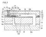
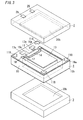
- a ferroelectric device according to the present embodiment will be explained below referring to Figs. 1A, 1B , 2 and 3 .
- a main unit 1 of the ferroelectric device comprises: a silicon substrate (hereinafter, called a first silicon substrate) 10; a first electrode 14a formed on one surface side of the first silicon substrate 10; a ferroelectric film 14b formed on a surface of the first electrode 14a opposite to the first silicon substrate 10 side; and a second electrode 14c formed on a surface of the ferroelectric film 14b opposite to the first electrode 14a side. That is, in Fig. 1B , the first electrode 14a is located on a lower surface side of the ferroelectric film 14b, as a lower electrode. The second electrode 14c is located on an upper surface side of the ferroelectric film 14b, as an upper electrode.
- the first electrode 14a and the second electrode 14c are called the lower electrode 14a and the upper electrode 14c, respectively.
- a monocrystal silicon substrate is used as the first silicon substrate 10 and the one surface of the first silicon substrate 10 is formed with a (100) face.
- the ferroelectric film 14b is formed of a ferroelectric material with a lattice constant difference from silicon.
- the ferroelectric device according to the present embodiment is a power generating device that converts vibration energy due to arbitrary vibration, such as automotive vibration, vibration caused by human motion or the like, into electric energy. Then, the ferroelectric film 14b constitutes a piezoelectric membrane.
- the main unit 1 further comprises a shock absorbing layer 14d.
- the shock absorbing layer 14d is located between the silicon substrate 10 and the lower electrode 14a (more specifically, is located directly below the lower electrode 14a), and is formed of a material with better lattice matching with the ferroelectric film 14b than silicon.
- the first silicon substrate 10 is provided with a cavity 10a that exposes a part of a surface of the shock absorbing layer 14d opposite to the lower electrode 14a side (that is, a part of a lower surface of the shock absorbing layer 14d).
- insulation films 19a, 19b are formed of silicon dioxide films and are provided on the one surface side and the other surface side of the first silicon substrate 10, respectively.
- the shock absorbing layer 14d is formed on a surface side of the first insulation film 19a that is located in the one surface side of the first silicon substrate 10.
- the main unit 1 is formed by using micro machining technology or the like, and then, as shown in Fig. 1A , comprises a frame portion 11 that has a frame-shape, and a weight portion 13 that is disposed within the frame portion 11.
- the weight portion 13 is swingably supported by the frame portion 11 through a cantilever 12 that is disposed on the one surface side of the first silicon substrate 10. Further, a functional portion 14 provided with the abovementioned lower electrode 14a, ferroelectric film 14b and upper electrode 14c is formed on the cantilever 12.
- the functional portion 14 constitutes a power generating part (a piezoelectric transforming part) that generates an AC voltage in response to vibration of the cantilever 12.
- a part of the second insulation film 19b, a part of the first silicon substrate 10, a part of the first insulation film 19a and a part of the shock absorbing layer 14d constitutes the abovementioned frame portion 11 and weight portion 13.
- the shock absorbing layer 14d constitutes the cantilever 12.
- the main unit 1 further includes pads 17a, 17c.
- the pads 17a, 17c are formed at regions corresponding to the frame portion 11, and are electrically connected to the lower electrode 14a and the upper electrode 14c through metallic wiring 16a, 16c, respectively.
- the main unit 1 includes the metallic wiring 16c and an insulation layer 18 that are provided on the one surface side of the first silicon substrate 10.
- the metallic wiring 16c defines an area in which the upper electrode 14c contacts the ferroelectric film 14b, and is electrically connected to the upper electrode 14c.
- the insulation layer 18 is formed so as to cover a periphery of the lower electrode 14a and a periphery of the ferroelectric film 14b, thereby preventing short circuit generated between the metallic wiring 16c and the lower electrode 14a. Further, the insulation layer 18 is formed over a wide region of the frame portion 11, and the pads 17a, 17c are formed on the insulation layer 18.
- the insulation layer 18 is formed of a silicon dioxide film, but is not limited to this configuration. For example, the insulation layer 18 may be formed of a silicon nitride film. Then, the first silicon substrate 10 and the functional portion 14 are electrically insulated from each other through the first insulation film 19a.
- the metallic wiring 16c and the upper electrode 14c of the present embodiment are formed of the same one member, but are not limited to this configuration.
- the metallic wiring 16c and the upper electrode 14c may be formed of different members.
- the main unit 1 includes a reinforcement layer 15 that is provided on the one surface side of the first silicon substrate 10.
- the reinforcement layer 15 is laminated on a laminated structure provided with the shock absorbing layer 14d, the lower electrode 14a, the ferroelectric film 14b and the upper electrode 14c, thereby reinforcing the laminated structure (in Figs. 1A and 3 , the graphic display of the reinforcement layer 15 is omitted).
- the reinforcement layer 15 is formed over a periphery of the functional portion 14, the frame portion 11 and the weight portion 13.
- a material that has good matching with so-called semiconductor process is used.
- the reinforcement layer 15 can be formed of an insulation material including polyimide, fluorine series resin or the like.
- the ferroelectric device as shown in Figs. 2 and 3 , includes a first cover substrate 2 that is fixed to the frame portion 11, in one surface side of the main unit 1. Further, the ferroelectric device includes a second cover substrate 3 that is fixed to the frame portion 11, in the other surface side of the main unit 1.
- the first cover substrate 2 is formed using a second silicon substrate 20. Then, a recess 20b is formed in one surface of the second silicon substrate 20 facing the main unit 1. Thereby, a displacement space for a movable portion 123 consisting of the cantilever 12 and the weight portion 13 is provided between the second silicon substrate 20 and the main unit 1.
- external connection electrodes 25, 25 are formed in the other surface side of the second silicon substrate 20, and are electrically connected to the functional portion 14.
- the external connection electrodes 25, 25 function as output electrodes for supplying, to the exterior, the AC voltage generated by the power generating part that is the functional portion 14.
- the external connection electrodes 25, 25 are electrically connected to access electrodes 24, 24 that are formed on the one surface side of the second silicon substrate 20, through through-hole wirings 23, 23 that penetrate to be installed in a thickness direction of the second silicon substrate 20, respectively.
- the access electrodes 24, 24 are bonded to the pads 17a, 17c in the main unit 1, thereby being electrically connected, respectively.
- each of the external connection electrodes 25, 25 and the access electrodes 24, 24 is constituted by a laminated film comprising a Ti film and an Au film.
- these materials are not limited especially.
- Cu is used as a material of each through-hole wiring 23, but the material is not limited to Cu.
- Ni, Al or the like may be used as the material.
- the first cover substrate 2 is provided with an insulation film 22, thereby preventing short circuit generated between the external connection electrodes 25, 25.
- the insulation film 22 is formed of a silicon dioxide film, and is provided over the one surface side and the other surface side of the second silicon substrate 20 and inner peripheries of through holes 21 in which the through-hole wirings 23, 23 are provided. Further, the first cover substrate 2 may be formed by using an insulation substrate, such as a glass substrate, stead of the second silicon substrate 20. In this case, the insulation film 22 is not required.
- the second cover substrate 3 is formed using a third silicon substrate 30. Then, a recess 30b is formed in one surface of the third silicon substrate 30 facing the main unit 1. Thereby, a displacement space for the movable portion 123 is provided between the third silicon substrate 30 and the main unit 1. Further, the second cover substrate 3 may be formed by using an insulation substrate, such as a glass substrate, stead of the third silicon substrate 30.
- a first bonding metal layer 118 for being bonded to the first cover substrate 2 is formed on the one surface side of the first silicon substrate 10.
- a second bonding metal layer 128 for being bonded to the first bonding metal layer 118 is formed on the one surface side of the second silicon substrate 20 (see Fig. 2 ).
- the same material as the pad 17c is used as a material of the first bonding metal layer 118.
- the first bonding metal layer 118 is formed on the one surface side of the first silicon substrate 10 so as to have the same thickness as the pad 17c. Further, the first bonding metal layer 118 is formed onto the insulation layer 18.
- the main unit 1 is bonded to each of the cover substrates 2, 3 by using a room temperature bonding method.
- the bonding method is not limited to the room temperature bonding method.
- the main unit 1 may be bonded by using a direct bonding method in which appropriate heating is performed, a resin bonding method using an epoxy resin or the like, or an anodic bonding method.
- the bonding temperature can be reduced more than the case where a thermal curing type of a resin adhesive (for example, a thermal curing type of an epoxy resin adhesive or the like) is used.
- the functional portion 14 is constituted by the lower electrode 14a, the ferroelectric film 14b that is a piezoelectric membrane, and the upper electrode 14c. Therefore, the ferroelectric film 14b of the functional portion 14 receives a stress caused by vibration of the cantilever 12, and the bias of electric charge is generated in the upper electrode 14c and the lower electrode 14a, and then an AC voltage is generated in the functional portion 14.
- PZT that is a type of a lead-based oxide ferroelectric is used as a ferroelectric material of the ferroelectric film 14b, and further, a monocrystal silicon substrate is used as the first silicon substrate 10 and the one surface of the first silicon substrate 10 is formed with a (100) face.
- the lead-based oxide ferroelectric is not limited to PZT.
- PZT-PMN (:Pb(Mn,Nb)O3) or PZT including other impurities may be adopted.
- the ferroelectric material of the ferroelectric film 14b is a ferroelectric material (the lead-based oxide ferroelectric, such as PZT, PZT-PMN or PZT including other impurities) with a lattice constant difference from silicon.
- Pt is used as the material of the lower electrode 14a
- Au is used as the material of the upper electrode 14c.
- these materials are not limited especially.
- Au, Al or Ir may be used as the material of the lower electrode 14a
- Mo, Al or Pt may be used as the material of the upper electrode 14c.
- the material of the shock absorbing layer 14d SrRuO3 is used, but the material is not limited to this.
- (Pb,La)TiO3, PbTiO3, MgO, LaNiO3 or the like may be used.
- the shock absorbing layer 14d may be constituted by a laminated film that comprises a Pt film and a SrRuO3 film.
- the shock absorbing layer 14d has a thickness of 2 ⁇ m
- the lower electrode 14a has a thickness of 500nm
- the ferroelectric film 14b has a thickness of 600nm
- the upper electrode 14c has a thickness of 100nm.
- these numerical values are one example, and are not limited especially.
- P is proportional to e 31 2/ ⁇ , where "e 31 " is a piezoelectric constant of the ferroelectric film 14b.
- the power generation efficiency increases with increase in the power generating index P.
- the insulation films 19a of a silicon dioxide film is formed on the entire surface of the one surface side of the first silicon substrate 10, and the insulation films 19b of a silicon dioxide film is formed on the entire surface of the other surface side of the first silicon substrate 10.
- the shock absorbing layer 14d is deposited on the entire surface of the one surface side of the first silicon substrate 10 (in this case, onto the first insulation film 19a), by using a sputtering method, a CVD method, an evaporation method or the like.
- the lower electrode 14a is deposited on the entire surface of the shock absorbing layer 14d opposite to the first silicon substrate 10 side, by using a sputtering method, a CVD method, an evaporation method or the like.
- the ferroelectric film 14b is deposited on the entire surface of the lower electrode 14a opposite to the shock absorbing layer 14d side, by using a sputtering method, a CVD method, a sol-gel method or the like.
- patterning of the ferroelectric film 14b is performed by using photolithography technology and etching technology, and then, patterning of the lower electrode 14a is performed by using photolithography technology and etching technology.
- a part of the lower electrode 14a is formed into a predetermined shape through the patterning, and the remaining part of the electrode 14a is kept in the same status as before the patterning, as the metallic wiring 16a.
- the part of the lower electrode 14a to which the patterning was performed and the metallic wiring 16a can be also considered as one lower electrode 14a.
- the insulation layer 18 is formed into a predetermined shape on the one surface side of the first silicon substrate 10. Then, the upper electrode 14c, the metallic wiring 16c, the pads 17a, 17c and the first bonding metal layer 118 are formed by using thin-film formation technology such as a sputtering method or CVD method, photolithography technology and etching technology. Then, the reinforcement layer 15 of a polyimide layer is formed. In the formation of the predetermined-shaped insulation layer 18, the insulation layer 18 is deposited on the entire surface of the one surface side of the first silicon substrate 10 by using a CVD method, and then patterning of the layer 18 is performed by using photolithography technology and etching technology.
- thin-film formation technology such as a sputtering method or CVD method, photolithography technology and etching technology.
- the reinforcement layer 15 of a polyimide layer is formed.
- the insulation layer 18 is deposited on the entire surface of the one surface side of the first silicon substrate 10 by using a CVD method, and then patterning of
- the insulation layer 18 may be formed by using lift-off technology. Further, in the formation of the reinforcement layer 15, when for example photosensitive polyimide is used as the material of the reinforcement layer 15, coating, photographic exposure, development, curing and the like of polyimide may be performed sequentially.
- the material and formation method of the reinforcement layer 15 are one example, and are not limited especially.
- the first silicon substrate 10 and the insulation films 19a, 19b are processed by using photolithography technology and etching technology, and thereby the frame portion 11, the cantilever 12 and the weight portion 13 are formed and the main unit 1 is formed.
- the first silicon substrate 10 is etched from the other surface side, through the reactive ion etching using SF6 gas or the like as the etching gas, and then the selective etching that uses the first insulation film 19a as an etching stopper layer is performed.
- the first insulation film 19a is etched from the other surface side of the first silicon substrate 10, through the reactive and anisotropic etching using fluorine series gas, chlorine-based gas or the like as the etching gas, and then the selective etching that uses the shock absorbing layer 14d as an etching stopper layer is performed. Then, the shock absorbing layer 14d is etched through the mechanical etching (the sputter etching) that uses only argon gas as the etching gas, in regard to the etching of unwanted parts of the layer 14d.
- the mechanical etching the sputter etching
- the cover substrates 2, 3 are bonded to the main unit 1, thereby obtaining the ferroelectric device having the configuration shown in Fig. 2 .
- the manufacturing is performed at the wafer level until the bonding process of the cover substrates 2, 3 to the main unit 1 is completed (that is, a silicon wafer is used about each of the silicon substrates 10, 20 and 30), and after that, the dicing process is performed, thereby dividing to each ferroelectric device.
- the cover substrates 2, 3 bonded to the main unit 1 may be formed by using appropriately widely know process, such as a photolithography process, an etching process, a thin-film formation process or a plating process.
- the cover substrates 2, 3 in the ferroelectric device are not indispensable.
- the ferroelectric device may be provided with only one of the cover substrates 2, 3, or may be provided with none of the cover substrates 2, 3.
- the shock absorbing layer 14d can be used as an etching stopper layer. Then, a part of the shock absorbing layer 14d that is exposed through the cavity 10a can directly become the cantilever 12 (a thin portion). Accordingly, with respect to a portion (in this case, the shock absorbing layer 14d) formed directly below the functional portion 14 including the lower electrode 14a, the ferroelectric film 14b and the upper electrode 14c, the reproducibility of the thickness can be improved without using a SOI substrate that is more extremely-expensive than the first silicon substrate 10.
- the thickness variation can be reduced in a surface of one silicon wafer in which a plurality of main units 1 are formed. That is, when the cavity 10a is formed, the selective etching that uses the shock absorbing layer 14d as an etching stopper layer is eventually performed. Accordingly, the thickness variation within a surface of the portion formed directly below the functional portion 14 is almost determined by the thickness variation within a surface of the shock absorbing layer 14d when the layer 14d is deposited.
- the ferroelectric device of the present embodiment comprises: the silicon substrate 10; the lower electrode 14a formed on the one surface side of the first silicon substrate 10; the ferroelectric film 14b formed on a surface of the lower electrode 14a opposite to the first silicon substrate 10 side; and the upper electrode 14c formed on a surface of the ferroelectric film 14b opposite to the lower electrode 14a side.
- the ferroelectric film 14b is formed of a ferroelectric material with a lattice constant difference from silicon.
- the ferroelectric device further comprises a shock absorbing layer 14d formed of a material with better lattice matching with the ferroelectric film 14b than silicon and provided directly below the lower electrode 14a.
- the silicon substrate 10 is provided with a cavity 10a that exposes a surface of the shock absorbing layer 14d opposite to the lower electrode 14a side. Therefore, when the cavity 10a is formed, the shock absorbing layer 14d can be used as an etching stopper layer. And then, a part of the shock absorbing layer 14d that is exposed through the cavity 10a can directly become the cantilever 12 (a thin portion). Accordingly, the crystallinity and the performance (in this case, piezoelectric constant e 31 ) of the ferroelectric film 14b can be improved, and the power generating property (the power generation efficiency or the like) that is the device property can be improved at low cost.
- the ferroelectric device of the present embodiment comprises a reinforcement layer 15 provided on the one surface side of the first silicon substrate 10.
- the reinforcement layer 15 is laminated on at least a part of a laminated structure provided with the shock absorbing layer 14d, the lower electrode 14a, the ferroelectric film 14b and the upper electrode 14c, thereby reinforcing the laminated structure. Therefore, the ferroelectric device can prevent each of the shock absorbing layer 14d, the lower electrode 14a, the ferroelectric film 14b and the upper electrode 14c from being damaged or cracked by vibration.
- the cantilever 12 constituted by a part of the shock absorbing layer 14d can be prevented from being damaged, and reliability can be increased.
- a conductive material such as SrRuO3, is used as the material of the shock absorbing layer 14d. Therefore, the ferroelectric device can efficiently take out an electric field generated by twist when the cantilever 12 vibrates, and the power generating property that is the device property can be improved.
- the abovementioned first insulation film 19a is not indispensable.
- the selective etching that uses the shock absorbing layer 14d as an etching stopper layer may be performed.
- a conductive material is adopted as the material of the shock absorbing layer 14d, and the lower electrode 14a is permitted to have the same electric potential as the first silicon substrate 10, the first insulation film 19a is not required.
- the first insulation film 19a is not required.
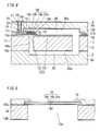
- the basic configuration of a ferroelectric device of the present embodiment is substantially identical to that of the First Embodiment. As shown Fig. 4 , the difference therebetween is that a second shock absorbing layer 14e is provided between the ferroelectric film 14b and the lower electrode 14a, in addition to the shock absorbing layer 14d (hereinafter, called a first shock absorbing layer) provided directly below the lower electrode 14a.
- the second shock absorbing layer 14e is formed of a material with better lattice matching with the ferroelectric film 14b than the lower electrode 14a.
- a method for manufacturing the ferroelectric device of the present embodiment is substantially identical to that explained in the First Embodiment.
- the difference therebetween is that the lower electrode 14a is formed on the entire surface of the one surface side of the silicon substrate 10, and the second shock absorbing layer 14e is then formed on the entire surface of the one surface side of the silicon substrate 10, and the ferroelectric film 14b is then formed on the entire surface of the one surface side of the silicon substrate 10.
- the material of the second shock absorbing layer 14e may be identical to or different from that of the first shock absorbing layer 14d. However, it is preferred that at least the second shock absorbing layer 14e is a conductive material.
- the ferroelectric device of the present embodiment further comprises the second shock absorbing layer 14e provided directly below the ferroelectric film 14b. Therefore, the ferroelectric device of the present embodiment can improve the crystallinity of the ferroelectric film 14b more than that of the First Embodiment.
- a ferroelectric device according to the present embodiment will be explained below referring to Fig. 5 .
- a ferroelectric device of the present embodiment comprises: a silicon substrate 10; a lower electrode 14a formed on one surface side of the silicon substrate 10; a ferroelectric film 14b formed on a surface of the lower electrode 14a opposite to the silicon substrate 10 side; and an upper electrode 14c formed on a surface of the ferroelectric film 14b opposite to the lower electrode 14a side.
- a monocrystal silicon substrate is used as the silicon substrate 10 and the one surface of the silicon substrate 10 is formed with a (100) face.
- the ferroelectric film 14b is formed of a ferroelectric material with a lattice constant difference from Si. Then, in the ferroelectric device, the constituent elements same as those of the First Embodiment are assigned with same reference numerals.
- the ferroelectric device of the present embodiment is a pyroelectric infrared sensor, and the ferroelectric film 14b constitutes a pyroelectric film.
- a shock absorbing layer 14d is provided directly below the lower electrode 14a and is formed of a material with better lattice matching with the ferroelectric film 14b than silicon.
- the silicon substrate 10 is provided with a cavity 10a that exposes a part of a surface of the shock absorbing layer 14d opposite to the lower electrode 14a side.
- insulation films 19a, 19b are formed of silicon dioxide films and are provided on the one surface side and the other surface side of the silicon substrate 10, respectively.
- the shock absorbing layer 14d is formed on a surface side of the first insulation film 19a which is located in the one surface side of the silicon substrate 10.
- PZT that is a type of a lead-based oxide ferroelectric is used as a ferroelectric material (a pyroelectric material) of the ferroelectric film 14b.
- the lead-based oxide ferroelectric is not limited to PZT.
- PZT-PLT, PLT, PZT-PMN or PZT-based ferroelectric including other impurities may be adopted.
- the pyroelectric material of the ferroelectric film 14b is a ferroelectric material (the lead-based oxide ferroelectric, such as PZT, PZT-PMN or PZT including other impurities) with a lattice constant difference from silicon that is a material of the silicon substrate 10.
- the material of the shock absorbing layer 14d SrRuO3 is used, but the material is not limited to this.
- (Pb,La)TiO3, PbTiO3, MgO, LaNiO3 or the like may be used.
- the shock absorbing layer 14d may be constituted by a laminated film that comprises a Pt film and a SrRuO3 film.
- Pt is used as the material of the lower electrode 14a.
- An infrared absorbing material having the conductive property such as Ni-Cr, Ni or Au-black, is used as the material of the upper electrode 14c.
- a functional portion 14, being a sensing element is constituted by the lower electrode 14a, the pyroelectric thin film 14b and the upper electrode 14c.
- these materials are not limited especially.
- Au, Al or Cu may be used as the material of the lower electrode 14a.
- the upper electrode 14c doubles as an infrared absorbing film.
- the cavity 10a constitutes a cavity for obtaining heat insulation between the functional portion 14 and the silicon substrate 10.
- the ferroelectric device includes a reinforcement layer 15 that is provided on the one surface side of the silicon substrate 10.
- the reinforcement layer 15 is laminated on a laminated structure provided with the shock absorbing layer 14d, the lower electrode 14a, the ferroelectric film 14b and the upper electrode 14c, thereby reinforcing the laminated structure.
- the reinforcement layer 15 is formed over a periphery of the functional portion 14 and the one surface of the silicon substrate 10 around the cavity 10a.
- a material that has good matching with so-called semiconductor process is used.
- the reinforcement layer 15 can be also formed of an insulation material including polyimide, fluorine series resin or the like.
- the enhancement of the heat insulation property between the functional portion 14 and the silicon substrate 10 is required in order to improve the sensor property. Therefore, it is preferred that the material of the shock absorbing layer 14d has lower thermal conductivity than silicon. It is known that the thermal conductivity of silicon is about 145-156 W/m.K. On the other hand, it is known that the thermal conductivity of SrRuO3 is about 5.97 W/m.K.
- the shock absorbing layer 14d has a thickness of 1 ⁇ m-2 ⁇ m
- the lower electrode 24a has a thickness of 100nm
- the ferroelectric film 24b has a thickness of 1 ⁇ m-3 ⁇ m
- the upper electrode 24c has a thickness of 50nm.
- these numerical values are one example, and are not limited especially.
- the ferroelectric device of the present embodiment is the pyroelectric infrared sensor, as explained above. Then, when a pyroelectric coefficient of the ferroelectric film 14b is denoted by ⁇ [C/(cm 2 ⁇ K)], an electric permittivity is denoted by " ⁇ " and an performance index of the pyroelectric infrared sensor (the pyroelectric device) is denoted by F ⁇ [C/(cm 2 ⁇ J)], F ⁇ is proportional to ⁇ / ⁇ . Therefore, the performance index F ⁇ increases with increase in the pyroelectric coefficient ⁇ of the ferroelectric film 14b.
- the insulation films 19a of a silicon dioxide film is formed on the entire surface of the one surface side of the silicon substrate 10 and the insulation films 19b of a silicon dioxide film is formed on the entire surface of the other surface side of the silicon substrate 10.
- the shock absorbing layer 14d is deposited on the entire surface of the one surface side of the silicon substrate 10 (in this case, onto the first insulation film 19a), by using a sputtering method, a CVD method, an evaporation method or the like.
- the lower electrode 14a is deposited on the entire surface of the shock absorbing layer 14d opposite to the silicon substrate 10 side, by using a sputtering method, a CVD method, an evaporation method or the like.
- the ferroelectric film 14b is deposited on the entire surface of the lower electrode 14a opposite to the shock absorbing layer 14d side, by using a sputtering method, a CVD method, a sol-gel method or the like.
- patterning of the ferroelectric film 14b is performed by using photolithography technology and etching technology, and then, patterning of the lower electrode 14a is performed by using photolithography technology and etching technology.
- the upper electrode 14c is formed into a predetermined shape on the one surface side of the silicon substrate 10, by using thin-film formation technology, such as a sputtering method or a CVD method, photolithography technology and etching technology.
- the reinforcement layer 15 of a polyimide layer is formed.
- coating, photographic exposure, development, curing and the like of polyimide may be performed sequentially.
- the abovementioned material and formation method of the reinforcement layer 15 are one example, and are not limited especially.
- the silicon substrate 10 and the insulation films 19a, 19b are processed by using photolithography technology and etching technology, and thereby the cavity 10a is formed.
- the silicon substrate 10 is etched from the other surface side, through the reactive ion etching using SF6 gas or the like as the etching gas, and then the selective etching that uses the first insulation film 19a as an etching stopper layer is performed.
- the first insulation film 19a is etched from the other surface side of the silicon substrate 10, through the reactive and anisotropic etching using fluorine series gas, chlorine-based gas or the like as the etching gas, and then the selective etching that uses the shock absorbing layer 14d as an etching stopper layer is performed.
- the manufacturing is performed at the wafer level until the formation process of the cavity 10a is completed, and after that (that is, after a plurality of ferroelectric devices are formed in a silicon wafer), the dicing process is performed, thereby dividing to each ferroelectric device.
- the shock absorbing layer 14d can be used as an etching stopper layer. Accordingly, with respect to a portion (in this case, the shock absorbing layer 14d) formed directly below the functional portion 14 including the lower electrode 14a, the ferroelectric film 14b and the upper electrode 14c, the reproducibility of the thickness can be improved without using a SOI substrate that is more extremely-expensive than the silicon substrate 10. Furthermore, with respect to the portion (in this case, only the shock absorbing layer 14d) formed directly below the functional portion 14, the thickness variation can be reduced in a surface of one silicon wafer in which a plurality of pyroelectric infrared sensors are formed.
- the selective etching that uses the shock absorbing layer 14d as an etching stopper layer is eventually performed. Accordingly, the thickness variation within a surface of the portion formed directly below the functional portion 14 is almost determined by the thickness variation within a surface of the shock absorbing layer 14d when the layer 14d is deposited.
- the ferroelectric device of the present embodiment comprises: the silicon substrate 10; the lower electrode 14a formed on the one surface side of the silicon substrate 10; the ferroelectric film 14b formed on a surface of the lower electrode 14a opposite to the silicon substrate 10 side; and the upper electrode 14c formed on a surface of the ferroelectric film 14b opposite to the lower electrode 14a side.
- the ferroelectric film 14b is formed of a ferroelectric material with a lattice constant difference from silicon.
- the ferroelectric device further comprises the shock absorbing layer 14d formed of a material with better lattice matching with the ferroelectric film 14b than silicon and provided directly below the lower electrode 14a.
- the silicon substrate 10 is provided with the cavity 10a exposing a surface of the shock absorbing layer 14d opposite to the lower electrode 14a side. Therefore, when the cavity 10a is formed, the shock absorbing layer 14d can be used as an etching stopper layer. Accordingly, the crystallinity and the performance (in this case, the pyroelectric coefficient ⁇ ) of the ferroelectric film 14b can be improved, and the device property (in this case, the performance index and the response speed) can be improved at low cost.
- the ferroelectric device of the present embodiment further comprises the reinforcement layer 15 provided on the one surface side of the silicon substrate 10.
- the reinforcement layer 15 is laminated on at least a part of a laminated structure provided with the shock absorbing layer 14d, the lower electrode 14a, the ferroelectric film 14b and the upper electrode 14c, thereby reinforcing the laminated structure. Therefore, the ferroelectric device can prevent each of the shock absorbing layer 14d, the lower electrode 14a, the ferroelectric film 14b and the upper electrode 14c from being damaged or cracked by vibration.
- a conductive material such as SrRuO3, is used as the material of the shock absorbing layer 14d. Therefore, the device property can be improved.
- the abovementioned first insulation film 19a is not indispensable.
- the selective etching that uses the shock absorbing layer 14d as an etching stopper layer may be performed.
- a conductive material is adopted as the material of the shock absorbing layer 14d and the lower electrode 14a is permitted to have the same electric potential as the silicon substrate 10
- the first insulation film 19a is not required.
- a plurality of functional portions 14 are provided on the one surface side of one silicon substrate 10 and a plurality of lower electrodes 14a of the functional portions 14 are configured so as to have the same electric potential as each other, the first insulation film 19a is not required.
- the ferroelectric device having the configuration shown in the above mentioned Fig. 5 is a pyroelectric infrared sensor including one functional portion 14, being a sensing element.
- the device is not limited to such a pyroelectric infrared sensor.
- the device may be a pyroelectric infrared sensor in which a plurality of functional portions 14 are arranged in two-dimensional array.
- a second shock absorbing layer 14e may be provided between the ferroelectric film 14b and the lower electrode 14a, in addition to the shock absorbing layer 14d (a first shock absorbing layer) provided directly below the lower electrode 14a, as is the case with the Second Embodiment.
- the second shock absorbing layer 14e is formed of a material with better lattice matching with the ferroelectric film 14b than the lower electrode 14a.
Landscapes
- Physics & Mathematics (AREA)
- General Physics & Mathematics (AREA)
- Engineering & Computer Science (AREA)
- Spectroscopy & Molecular Physics (AREA)
- Power Engineering (AREA)
- Mechanical Engineering (AREA)
- Manufacturing & Machinery (AREA)
- Microelectronics & Electronic Packaging (AREA)
- Micromachines (AREA)
- Photometry And Measurement Of Optical Pulse Characteristics (AREA)
- General Electrical Machinery Utilizing Piezoelectricity, Electrostriction Or Magnetostriction (AREA)
Applications Claiming Priority (2)
| Application Number | Priority Date | Filing Date | Title |
|---|---|---|---|
| JP2010098204A JP5632643B2 (ja) | 2010-04-21 | 2010-04-21 | 強誘電体デバイス |
| PCT/JP2011/059521 WO2011132636A1 (fr) | 2010-04-21 | 2011-04-18 | Dispositif ferroélectrique |
Publications (2)
| Publication Number | Publication Date |
|---|---|
| EP2562837A1 true EP2562837A1 (fr) | 2013-02-27 |
| EP2562837A4 EP2562837A4 (fr) | 2014-03-19 |
Family
ID=44834155
Family Applications (1)
| Application Number | Title | Priority Date | Filing Date |
|---|---|---|---|
| EP11771971.6A Withdrawn EP2562837A4 (fr) | 2010-04-21 | 2011-04-18 | Dispositif ferroélectrique |
Country Status (7)
| Country | Link |
|---|---|
| US (1) | US20130032906A1 (fr) |
| EP (1) | EP2562837A4 (fr) |
| JP (1) | JP5632643B2 (fr) |
| KR (1) | KR101382516B1 (fr) |
| CN (1) | CN102859735B (fr) |
| TW (1) | TWI437741B (fr) |
| WO (1) | WO2011132636A1 (fr) |
Families Citing this family (18)
| Publication number | Priority date | Publication date | Assignee | Title |
|---|---|---|---|---|
| JP2013110920A (ja) * | 2011-11-24 | 2013-06-06 | Panasonic Corp | 発電装置 |
| JP5943506B2 (ja) * | 2011-12-09 | 2016-07-05 | 浩平 速水 | 振動力発電装置 |
| JP5023244B1 (ja) * | 2012-01-13 | 2012-09-12 | 浩平 速水 | 振動力発電装置 |
| JP2013195212A (ja) * | 2012-03-19 | 2013-09-30 | Ngk Insulators Ltd | 薄板振動素子およびその製造方法 |
| WO2013145260A1 (fr) * | 2012-03-30 | 2013-10-03 | 富士通株式会社 | Dispositif électronique et procédé de fabrication de celui-ci |
| US10726231B2 (en) | 2012-11-28 | 2020-07-28 | Invensense, Inc. | Integrated piezoelectric microelectromechanical ultrasound transducer (PMUT) on integrated circuit (IC) for fingerprint sensing |
| US9511994B2 (en) | 2012-11-28 | 2016-12-06 | Invensense, Inc. | Aluminum nitride (AlN) devices with infrared absorption structural layer |
| US9114977B2 (en) * | 2012-11-28 | 2015-08-25 | Invensense, Inc. | MEMS device and process for RF and low resistance applications |
| US9618405B2 (en) | 2014-08-06 | 2017-04-11 | Invensense, Inc. | Piezoelectric acoustic resonator based sensor |
| US10497747B2 (en) * | 2012-11-28 | 2019-12-03 | Invensense, Inc. | Integrated piezoelectric microelectromechanical ultrasound transducer (PMUT) on integrated circuit (IC) for fingerprint sensing |
| TWI621242B (zh) * | 2013-09-19 | 2018-04-11 | 伊凡聖斯股份有限公司 | 具有紅外線吸收結構層的氮化鋁(ain)裝置 |
| US9574959B2 (en) * | 2014-09-02 | 2017-02-21 | Apple Inc. | Various stress free sensor packages using wafer level supporting die and air gap technique |
| US9862592B2 (en) * | 2015-03-13 | 2018-01-09 | Taiwan Semiconductor Manufacturing Co., Ltd. | MEMS transducer and method for manufacturing the same |
| JP6861558B2 (ja) * | 2017-03-31 | 2021-04-21 | ローム株式会社 | 超音波装置 |
| WO2018231210A1 (fr) * | 2017-06-14 | 2018-12-20 | Intel Corporation | Matériaux ferroélectriques en couche mince et leurs procédés de fabrication |
| JP7090249B2 (ja) * | 2019-06-06 | 2022-06-24 | 国立大学法人 東京大学 | 静電型デバイスを製造する製造方法 |
| JP2022090625A (ja) * | 2020-12-07 | 2022-06-17 | セイコーホールディングス株式会社 | 焦電センサ、焦電センサシステム及び焦電センサの製造方法 |
| CN113156230B (zh) * | 2021-01-13 | 2022-10-14 | 西安理工大学 | 一种摩擦电能量采集器测试装置及测试方法 |
Family Cites Families (22)
| Publication number | Priority date | Publication date | Assignee | Title |
|---|---|---|---|---|
| JP2866216B2 (ja) * | 1991-02-15 | 1999-03-08 | キヤノン株式会社 | カンチレバーの製造方法 |
| JPH08167740A (ja) * | 1994-12-10 | 1996-06-25 | Horiba Ltd | 焦電型赤外線薄膜素子 |
| KR0141160B1 (ko) * | 1995-03-22 | 1998-06-01 | 김광호 | 강유전체 메모리 장치 및 그 제조방법 |
| JP3409944B2 (ja) | 1995-05-26 | 2003-05-26 | 松下電器産業株式会社 | 強誘電体素子及びその製造方法 |
| JP2002214038A (ja) * | 2001-01-17 | 2002-07-31 | Matsushita Electric Ind Co Ltd | 焦電型赤外線検出素子の製造方法 |
| JP2004006722A (ja) * | 2002-03-27 | 2004-01-08 | Seiko Epson Corp | 圧電アクチュエータ、インクジェット式ヘッド及び吐出装置 |
| US7268472B2 (en) * | 2002-11-11 | 2007-09-11 | Seiko Epson Corporation | Piezoelectric device, liquid jetting head, ferroelectric device, electronic device and methods for manufacturing these devices |
| JP4058018B2 (ja) * | 2003-12-16 | 2008-03-05 | 松下電器産業株式会社 | 圧電素子及びその製造方法、並びにその圧電素子を備えたインクジェットヘッド、インクジェット式記録装置及び角速度センサ |
| JP4192794B2 (ja) * | 2004-01-26 | 2008-12-10 | セイコーエプソン株式会社 | 圧電素子、圧電アクチュエーター、インクジェット式記録ヘッド、インクジェットプリンター、表面弾性波素子、周波数フィルタ、発振器、電子回路、薄膜圧電共振器、及び電子機器 |
| JP2005294452A (ja) * | 2004-03-31 | 2005-10-20 | Fujitsu Ltd | 薄膜積層体、その薄膜積層体を用いたアクチュエータ素子、フィルター素子、強誘電体メモリ、および光偏向素子 |
| JP2008028030A (ja) * | 2006-07-19 | 2008-02-07 | Seiko Epson Corp | 圧電素子および液体噴射ヘッド |
| JP2008232896A (ja) * | 2007-03-22 | 2008-10-02 | Toyohashi Univ Of Technology | 薄膜赤外線検出素子およびその製造方法 |
| JP5391395B2 (ja) * | 2007-10-15 | 2014-01-15 | 日立金属株式会社 | 圧電薄膜付き基板及び圧電素子 |
| JP2009201101A (ja) * | 2008-01-21 | 2009-09-03 | Panasonic Electric Works Co Ltd | Baw共振装置およびその製造方法 |
| CA2664969C (fr) * | 2008-05-02 | 2011-09-20 | Francis V. Smith | Combinaison de vehicule-caravane de fort tonnage, elements de caravane et methode d'utilisation |
| JP5115330B2 (ja) * | 2008-05-22 | 2013-01-09 | セイコーエプソン株式会社 | 液体噴射ヘッドおよびそれを備えた液体噴射装置 |
| JP2010161330A (ja) * | 2008-12-08 | 2010-07-22 | Hitachi Cable Ltd | 圧電薄膜素子 |
| JP5452115B2 (ja) * | 2009-07-22 | 2014-03-26 | パナソニック株式会社 | 発電デバイス |
| JP2011071467A (ja) * | 2009-08-28 | 2011-04-07 | Panasonic Electric Works Co Ltd | 強誘電体デバイスの製造方法 |
| KR101561662B1 (ko) * | 2009-09-29 | 2015-10-21 | 삼성전자주식회사 | 곡선형 리드선들을 가진 압전형 마이크로 스피커 및 그 제조 방법 |
| JP2011091319A (ja) * | 2009-10-26 | 2011-05-06 | Panasonic Electric Works Co Ltd | 発電デバイス |
| JP2011091318A (ja) * | 2009-10-26 | 2011-05-06 | Panasonic Electric Works Co Ltd | 発電デバイス |
-
2010
- 2010-04-21 JP JP2010098204A patent/JP5632643B2/ja not_active Expired - Fee Related
-
2011
- 2011-04-18 KR KR1020127027356A patent/KR101382516B1/ko not_active Expired - Fee Related
- 2011-04-18 US US13/642,208 patent/US20130032906A1/en not_active Abandoned
- 2011-04-18 CN CN201180019864.2A patent/CN102859735B/zh not_active Expired - Fee Related
- 2011-04-18 WO PCT/JP2011/059521 patent/WO2011132636A1/fr not_active Ceased
- 2011-04-18 EP EP11771971.6A patent/EP2562837A4/fr not_active Withdrawn
- 2011-04-20 TW TW100113808A patent/TWI437741B/zh not_active IP Right Cessation
Also Published As
| Publication number | Publication date |
|---|---|
| CN102859735A (zh) | 2013-01-02 |
| KR101382516B1 (ko) | 2014-04-07 |
| WO2011132636A1 (fr) | 2011-10-27 |
| US20130032906A1 (en) | 2013-02-07 |
| JP2011228548A (ja) | 2011-11-10 |
| TWI437741B (zh) | 2014-05-11 |
| KR20120139825A (ko) | 2012-12-27 |
| CN102859735B (zh) | 2015-04-15 |
| EP2562837A4 (fr) | 2014-03-19 |
| TW201203638A (en) | 2012-01-16 |
| JP5632643B2 (ja) | 2014-11-26 |
Similar Documents
| Publication | Publication Date | Title |
|---|---|---|
| EP2562837A1 (fr) | Dispositif ferroélectrique | |
| US11165011B2 (en) | Piezoelectric element and method for manufacturing piezoelectric element | |
| Muralt | Ferroelectric thin films for micro-sensors and actuators: a review | |
| US20090302716A1 (en) | Piezoelectric device | |
| US20140035440A1 (en) | Piezoelectric device | |
| TWI455472B (zh) | 振動發電裝置 | |
| CN102859737B (zh) | 用于制造铁电器件的方法 | |
| US20130285507A1 (en) | Vibration power generating element and vibration power generating device using same | |
| JP5685719B2 (ja) | 振動発電素子およびそれを用いた振動発電装置 | |
| US11631800B2 (en) | Piezoelectric MEMS devices and methods of forming thereof | |
| US20140035439A1 (en) | Piezoelectric device | |
| US20210343929A1 (en) | Piezoelectric device | |
| US10608166B2 (en) | Method for manufacturing a piezoelectric device | |
| US11262246B2 (en) | Pyroelectric detection device with rigid membrane | |
| TWI455471B (zh) | 振動發電裝置及其製造方法 | |
| JP2011091319A (ja) | 発電デバイス | |
| JP2008227211A (ja) | 圧電装置の製造方法及び圧電装置 | |
| JP2011091318A (ja) | 発電デバイス | |
| US20210313960A1 (en) | Vibrator element | |
| WO2014020786A1 (fr) | Dispositif générateur d'électricité | |
| JP2015018830A (ja) | 発電デバイス | |
| JP2011091977A (ja) | 発電デバイス |
Legal Events
| Date | Code | Title | Description |
|---|---|---|---|
| PUAI | Public reference made under article 153(3) epc to a published international application that has entered the european phase |
Free format text: ORIGINAL CODE: 0009012 |
|
| 17P | Request for examination filed |
Effective date: 20121005 |
|
| AK | Designated contracting states |
Kind code of ref document: A1 Designated state(s): AL AT BE BG CH CY CZ DE DK EE ES FI FR GB GR HR HU IE IS IT LI LT LU LV MC MK MT NL NO PL PT RO RS SE SI SK SM TR |
|
| DAX | Request for extension of the european patent (deleted) | ||
| A4 | Supplementary search report drawn up and despatched |
Effective date: 20140217 |
|
| RIC1 | Information provided on ipc code assigned before grant |
Ipc: G01P 15/09 20060101ALI20140211BHEP Ipc: G01J 1/02 20060101ALI20140211BHEP Ipc: B81B 7/02 20060101ALI20140211BHEP Ipc: H01L 41/113 20060101AFI20140211BHEP Ipc: H01L 41/08 20060101ALI20140211BHEP Ipc: H01L 41/22 20130101ALI20140211BHEP Ipc: H01L 41/18 20060101ALI20140211BHEP |
|
| GRAP | Despatch of communication of intention to grant a patent |
Free format text: ORIGINAL CODE: EPIDOSNIGR1 |
|
| RIC1 | Information provided on ipc code assigned before grant |
Ipc: G01P 15/09 20060101ALI20150113BHEP Ipc: H02N 2/18 20060101ALI20150113BHEP Ipc: G01J 1/02 20060101ALI20150113BHEP Ipc: H01L 41/18 20060101ALI20150113BHEP Ipc: H01L 41/08 20060101ALI20150113BHEP Ipc: H01L 41/22 20130101ALI20150113BHEP Ipc: B81B 7/02 20060101AFI20150113BHEP Ipc: H01L 41/113 20060101ALI20150113BHEP |
|
| INTG | Intention to grant announced |
Effective date: 20150130 |
|
| RIN1 | Information on inventor provided before grant (corrected) |
Inventor name: MATSUSHIMA, TOMOAKI Inventor name: AIZAWA, KOICHI Inventor name: OGAWA, JUNYA Inventor name: YAMAUCHI, NORIHIRO |
|
| RAP1 | Party data changed (applicant data changed or rights of an application transferred) |
Owner name: PANASONIC INTELLECTUAL PROPERTY MANAGEMENT CO., LT |
|
| STAA | Information on the status of an ep patent application or granted ep patent |
Free format text: STATUS: THE APPLICATION IS DEEMED TO BE WITHDRAWN |
|
| 18D | Application deemed to be withdrawn |
Effective date: 20150610 |