EP2562872B1 - Antennenvorrichtung - Google Patents
Antennenvorrichtung Download PDFInfo
- Publication number
- EP2562872B1 EP2562872B1 EP20120005274 EP12005274A EP2562872B1 EP 2562872 B1 EP2562872 B1 EP 2562872B1 EP 20120005274 EP20120005274 EP 20120005274 EP 12005274 A EP12005274 A EP 12005274A EP 2562872 B1 EP2562872 B1 EP 2562872B1
- Authority
- EP
- European Patent Office
- Prior art keywords
- antenna
- ground layer
- dielectric plate
- board
- pattern
- Prior art date
- Legal status (The legal status is an assumption and is not a legal conclusion. Google has not performed a legal analysis and makes no representation as to the accuracy of the status listed.)
- Active
Links
Images


Classifications
-
- H—ELECTRICITY
- H01—ELECTRIC ELEMENTS
- H01Q—ANTENNAS, i.e. RADIO AERIALS
- H01Q9/00—Electrically-short antennas having dimensions not more than twice the operating wavelength and consisting of conductive active radiating elements
- H01Q9/04—Resonant antennas
- H01Q9/0407—Substantially flat resonant element parallel to ground plane, e.g. patch antenna
- H01Q9/0414—Substantially flat resonant element parallel to ground plane, e.g. patch antenna in a stacked or folded configuration
-
- H—ELECTRICITY
- H01—ELECTRIC ELEMENTS
- H01Q—ANTENNAS, i.e. RADIO AERIALS
- H01Q1/00—Details of, or arrangements associated with, antennas
- H01Q1/36—Structural form of radiating elements, e.g. cone, spiral, umbrella; Particular materials used therewith
- H01Q1/38—Structural form of radiating elements, e.g. cone, spiral, umbrella; Particular materials used therewith formed by a conductive layer on an insulating support
-
- H—ELECTRICITY
- H01—ELECTRIC ELEMENTS
- H01Q—ANTENNAS, i.e. RADIO AERIALS
- H01Q1/00—Details of, or arrangements associated with, antennas
- H01Q1/48—Earthing means; Earth screens; Counterpoises
-
- H—ELECTRICITY
- H01—ELECTRIC ELEMENTS
- H01Q—ANTENNAS, i.e. RADIO AERIALS
- H01Q9/00—Electrically-short antennas having dimensions not more than twice the operating wavelength and consisting of conductive active radiating elements
- H01Q9/04—Resonant antennas
- H01Q9/0407—Substantially flat resonant element parallel to ground plane, e.g. patch antenna
- H01Q9/045—Substantially flat resonant element parallel to ground plane, e.g. patch antenna with particular feeding means
Definitions
- the present invention relates to a radio-communication antenna device, particularly to an antenna device comprising a configuration of a patch antenna.
- a conductive layer that acts as an antenna pattern is formed in or on one of the surfaces of a dielectric plate, and a ground layer is formed in or on the other surface.
- the antenna pattern is electrically connected to a feed pin that is inserted into a middle substrate of the antenna board, and the feed pin is electrically connected to a coaxial cable that transmits a radio frequency (RF) signal.
- RF radio frequency
- US 5706015 discloses mobile radio antenna comprising a metal sheet plane parallel to the ground plane and spaced at a distance of 0.04 of an average operating wavelength of a mobile radio frequency band from the ground plane.
- US 4051477 discloses a radio frequency antenna structure wherein a raised pedestal portion of the ground plane surface is provided and above which pedestal portion a microstrip radiator is at a predetermined distance above the base ground plane to produce mirror image or apparent radiating aperture(s) there below.
- US 20060220977 discloses a loop antenna with a loop element and a parasitic element provided independently of this loop element on the same dielectric board to form an antenna element and sends or receives a circularly polarized wave by this antenna element, provides a metal plate parallel with or having a slight inclination with respect to the dielectric board, and sets this metal plate separated from the dielectric board by exactly a predetermined distance.
- Japanese Unexamined Patent Publication No. 4-337907 discloses a configuration of a basic antenna board. In the antenna board disclosed in Japanese Unexamined Patent Publication No. 4-337907 , a flexible board having a projected step portion at one end edge is integrally bonded without providing a ground layer in a rear surface of the antenna board. A microstrip line and the ground layer are extended to the projected step portion in a rear surface of the flexible board, and the projected step portion acts as a coaxial-cable connecting lead portion.
- Japanese Unexamined Patent Publication No. 2004-72320 discloses an antenna device including a dielectric plate in which the antenna pattern (described as a patch electrode) is provided in a ceiling surface, a circuit board on which a radio frequency circuit electrically connected to the antenna pattern is mounted, and a shield case that accommodates the circuit board.
- the antenna device a ceiling plate portion of the shield case is overhung to a surrounding area of a bottom surface of the dielectric plate, and the radio frequency signal is fed to the radio frequency circuit, whereby the shield case acts as a ground.
- a width of the antenna pattern be set to one half the length of a wavelength of the radio wave. It is also necessary that an overhang width (a width of a portion outside the end edge of the antenna pattern) of the ground layer to the antenna pattern be sufficiently increased. Specifically, it is necessary that the overhang width of the ground layer be at least one half of the width of the antenna pattern. Accordingly, each side of the dielectric plate is optimally set to at least the length (that is, double the width of the antenna pattern) corresponding to the wavelength of the radio wave.
- the size of the antenna pattern or the antenna board is determined with respect to the wavelength of the radio wave.
- the wavelength of the radio wave is shortened by a wavelength shortening effect of the dielectric material. Because the wavelength shortening effect increases with increasing permittivity, when the dielectric plate is made of high-permittivity material, the wavelength of the radio wave is largely shortened, and the size of the dielectric plate can be reduced according to the shortened wavelength.
- gain is decreased because the use of the high-permittivity board reduces an aperture area. In order to increase the gain, it is necessary to enlarge the dielectric plate. However, such a compact antenna device is not desired due to the high cost of the high-permittivity material.
- the dielectric plate is made of low-permittivity material, gain is enhanced, and the cost can be lowered.
- the wavelength of the radio wave cannot effectively be shortened, the size of the dielectric plate is hardly reduced.
- the present invention has been devised to solve the problems described above, and an object thereof is to provide a compact antenna device in which high gain is obtained at reasonable cost.
- an antenna device includes an antenna board in which an antenna pattern is formed in or on one of the surfaces of a dielectric plate while a ground layer is formed in or on the other surface, and a feed pin is disposed in a middle substrate or portion of the antenna device in order to feed electric power or a signal to the antenna pattern, wherein a metallic plate is disposed facing the ground layer side of the antenna board, and the metallic plate and the ground layer are coupled and electrically connected through a plurality of metallic spacers.
- the current passed through the ground layer by the generation of an electric field propagates partially to the spacers and the metallic plate, and the metal located within the propagation area acts as a ground connected to the ground layer. Therefore, the radiation efficiency can sufficiently be enhanced even if the overhang width of the ground layer to the antenna pattern is insufficient.
- the permittivity is relatively low, even if the dielectric plate is made of a material in which the wavelength shortening effect is low because of relatively-low permittivity, the length of one side of the dielectric plate can be made shorter than the wavelength of the radio wave, which allows production of a compact antenna board.
- the use of low-permittivity material can enlarge the antenna pattern even if the size of the board is reduced. That is, because the aperture area can be increased, high gain can be ensured. Additionally the cost can be lowered.
- the function of the ground is complemented by the shield case below the dielectric plate.
- the circuit board is disposed in the shield case, and the coaxial cable and the feed pin are connected through circuit board, which results in the complicated configuration.
- the antenna board and the metallic plate are coupled with spacers interposed therebetween, a simple configuration is achieved.
- the antenna device can easily be attached to a wall surface.
- a first conductor pattern is formed in a predetermined area comprising a connection point to the feed pin while separated from the ground layer in the ground-layer forming surface of the antenna board, and a second conductor pattern is formed near the first conductor pattern while separated from first conductor pattern and the ground layer.
- the first and second conductor patterns are connected in series through a capacitor.
- a coaxial cable is inserted into a gap between the antenna board and the metallic plate, and an inner conductor of the coaxial cable is connected to the second conductor pattern while an outer conductor of the coaxial cable is connected to the ground layer.
- the gain of the antenna is enhanced with increasing area of the dielectric plate, it is necessary to increase the thickness of the dielectric plate in order to ensure the gain without changing the area of the dielectric plate.
- the thickness of the dielectric plate is increased, because a reactance or resistance component is generated by the length of the feed pin, it is necessary to provide a circuit that cancels the reactance or resistance component.
- the inner conductor of the coaxial cable and the feed pin are connected in series through an impedance converting capacitor.
- the reactance or resistance component of the feed pin is cancelled by the capacitor, and the impedance of the RF-signal route in the antenna board can be matched with the impedance of the coaxial cable. Therefore, the gain can be enhanced by the thickness of the board without degrading the radiation efficiency.
- the function of the ground is complemented by the metallic spacers and the metallic plate coupled to the metallic spacers, and the radio wave can be radiated without trouble. Therefore, even if low-permittivity material is used, the size of the dielectric plate can be reduced, the gain can be enhanced, and, in addition, the cost can be reduced or maintained.
- Figs. 1A and 1 B each illustrate a configuration of a main part of an RFID-system antenna device according to an embodiment of the invention.
- Fig. 1 A is a side view of the main part
- Fig. 1 B is a front view of the main part.
- the main part of the antenna device of the embodiment comprises a coupled body of an antenna board 1 and a metallic plate 2.
- front-surface-side conductive layer 11 and rear-surface-side conductive layer 12 are formed in or on both surfaces of a square dielectric plate 10, in which the four corners are cut off.
- the front-surface-side conductive layer 11 has a circular shape, in which two arcs disposed opposite each other are notched, and acts as an antenna pattern.
- the rear-surface-side conductive layer 12 extends substantially the whole rear surface of dielectric plate 10 and acts as a ground layer.
- the antenna pattern 11 is not limited to a circular shape, but may have a square shape instead.
- Metallic plate 2 is a rectangular, plate-like body or substrate that is slightly larger in longitudinal and latitudinal (planar) directions than the antenna board 1.
- a lower surface of the ground layer 12 of the antenna board 1 is covered with a resist,except that the resist has been removed or was not applied in the areas where each spacer 3 is coupled to the ground layer 12. Therefore, the ground layer 12, the spacers 3, and the metallic plate 2 are integrated, and electrically connected.
- a passageway or conduit 13 comprising a conductor is positioned properly into and through dielectric substrate 10 in the antenna board 1, and the conduit 13 acts as a feed pin 13.
- the feed pin 13 is electrically connected to the antenna pattern 11.
- a coaxial cable 4 is inserted in a gap between the antenna board 1 and the metallic plate 2 to transmit an RF signal.
- the coaxial cable 4 is introduced near a connection point to the feed pin 13 along a rear surface of the antenna board 1, and an outer conductor and an inner conductor of the coaxial cable 4 are electrically connected to the ground layer 12 and the feed pin 13, respectively. Because of the connection, the RF signal is introduced to the antenna pattern 11 through the feed pin 13, and an electric field is generated between the antenna pattern 11 and the ground layer 12 to radiate a radio wave.
- A is a diameter of the antenna pattern 11 and B is a length of one side of the dielectric plate 10.
- a width length of the antenna pattern is set to one half of a wavelength ⁇ of the radio wave, and an overhang width of the ground layer to the antenna pattern is set to ⁇ /4 or more. Accordingly, it is necessary that one side of the dielectric plate 10 be at least the length of one wavelength.
- a current passed through the ground layer 12 propagates to the spacers 3 and the metallic plate 2, which are coupled to the ground layer 12, so that a metallic material located within an area of the current propagation can act as a ground connected to the ground layer 12.
- the current is efficiently passed along a lengthwise direction of the spacers 3 by forming the spacers 3 directly coupled to the ground layer 12 into a columnar shape, so that the ground layer 12 that is deficient in an area to radiate the radio wave can be complemented. Therefore, the radio wave can be stably radiated.
- the columnar spacer 3 is used.
- the spacers 3 having a prismatic column shape or a triangular prism shape may be used.
- the number of spacers 3 is not limited to four, but more than four spacers 3 may be provided.
- the spacers 3 or the metallic plate 2 There is no particular limitation to a material for the spacers 3 or the metallic plate 2.
- a material for the spacers 3 or the metallic plate 2 For example, iron, aluminum, and stainless steel may be used.
- the overhang width of the metallic plate 2 to the antenna board 1 can be adjusted as needed but not so much as to cause difficulty in supporting a later-described redome 6.
- the dielectric plate 10 is made of a material having a relatively low permittivity. Therefore, the size of the antenna board 1 can be reduced while gain is enhanced to lower the cost.
- the radio wave in the antenna board 1 is shortened according to the permittivity of the dielectric plate 10. Specifically, assuming that ⁇ r is permittivity, the shortened wavelength ⁇ becomes about 1/ ⁇ r times the original wavelength.
- the wavelength can largely be shortened.
- the length of one side of the dielectric plate 10 is set to at least the wavelength ⁇ of the radio wave.
- the wavelength of the radio wave is largely shortened using the high-permittivity dielectric plate 10, whereby the size of the dielectric plate 10 can be reduced while the desirable condition is satisfied.
- a radio wave in a UHF band (860 to 950 MHz) has a wavelength of about 30 cm, and the wavelength in the antenna board 1 is shortened to about 12 cm when the permittivity ⁇ r of the dielectric plate 10 is set to 6.
- the antenna pattern 11 having the diameter of 6 cm can be formed in or on the dielectric plate 10 having one side of 12 cm.
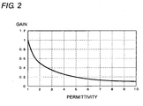
- the gain is largely decreased with increasing permittivity of the dielectric plate 10.
- Fig. 2 illustrates a relationship between the permittivity and the gain when a volume, a frequency band, and radiation efficiency of the antenna board 1 are kept constant.
- the gain is normalized with the gain having the permittivity of 1 (permittivity of air).
- the gain for the permittivity ⁇ r of 6 is lower than 0.2 times the gain for the permittivity of 1.
- the gain of the radio wave radiated from the antenna board 1 is substantially proportional to the volume of the dielectric plate 10. Accordingly, the gain significantly decreases with decreasing area of the high-permittivity dielectric plate 10. Because there is a restriction to the increase of the thickness of the dielectric plate 10, it is necessary to enlarge the surface area of the dielectric plate 10 in order to enhance the gain. However, in this case, the size of the dielectric plate 10 cannot be reduced.
- the dielectric plate 10 is made of low-permittivity material, the wavelength shortening effect of the radio wave is decreased while the gain can be enhanced. Accordingly, in this case the size of the antenna board 1 is hardly reduced.
- the function of the ground is complemented by the spacers 3 and the metallic plate 2, so that the length B of one side of the antenna board 1 can be made shorter than the wavelength ⁇ . Accordingly, even if the dielectric plate 10 is made of the relatively-low-permittivity material, the dielectric plate 10 can be reduced within an area where the diameter A of the antenna pattern 11 can be set to ⁇ /2. The gain can be enhanced by decreasing the permittivity.
- the gain is obtained about double that of the permittivity of 6.
- the permittivity ⁇ r is 3.5, because the wavelength of 30 cm can be shortened to about 16 cm, the diameter A of the antenna pattern 11 can be set to about 8 cm.
- the length of one side of the dielectric plate 10 made of the material having a permittivity ⁇ r of 3.5 is set to 12 cm that is equal to the wavelength shortened using the material having the permittivity ⁇ r of 6, the higher gain can be obtained compared with the permittivity ⁇ r of 6.
- one side of the dielectric plate 10 can be made shorter than 12 cm (however, more than 8 cm).
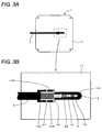
- a connection state between the antenna board 1 and the coaxial cable 4 will be described with reference to Figs. 3A and 3B .
- Fig. 3A illustrates an entire configuration of the rear surface of the antenna board 1 together in relationto the coaxial cable 4
- Fig. 3B is an enlarged view in the area (within the dotted-line frame in Fig. 3A ) of the point connected to the coaxial cable 4.
- a white portion 17 in Figs. 3A and 3B represents a resist that covers the ground layer 12; the actual resist has a green color.
- the resist 17 is removed in the area corresponding to a leading end portion of the coaxial cable 4 in addition to the areas coupled to the spacers 3, and the ground layer 12 is exposed in part of the area corresponding to the leading end portion of the coaxial cable 4A.
- Microstrip line 14 and a small conductor pattern 15 are formed in a band-shape region 101 beside the exposed portion with a micro gap.
- the feed pin 13 is provided by the passageway or conduit between the conductor pattern 15 and a point corresponding to the conductor pattern 15 on the front-surface side of dielectric plate 10.
- the microstrip line 14 and the conductor pattern 15 are electrically independent from the ground layer 12.
- conductive-layer removing regions 102, 103, and 104 are formed along a peripheral border of the ground layer 12, and the regions 102, 103, and 104 act as a thermal barrier or sink.
- the point where the ground layer 12 is exposed is coupled to the ground layer 12 at the point, where the resist 17 is covered, with the thermal lands 102, 103, and 104 interposed therebetween.
- An outer conductor 41 of the coaxial cable 4 is connected to the point where the ground layer 12 is exposed, and an inner conductor 42 of the coaxial cable 4 is connected to the microstrip line 14.
- the leading end portion of the microstrip line 14 and the conductor pattern 15 are connected to each other through the capacitor 5.
- the thickness of the dielectric plate 10 may be increased.
- the reactance or resistance component generated by the feed pin 13 is cancelled by the capacitor 5, and impedance of an RF signal route on the side of the antenna board 1 can be matched with impedance of the coaxial cable 4. Therefore, the radio wave from the antenna pattern 1 can be efficiently radiated.
- the microstrip line 14 and the conductor pattern 15 are integrated without the capacitor 5, and the inner conductor 42 of the coaxial cable 4 may be connected to the integrated microstrip line 14 and conductor pattern 15.
- Fig. 4 illustrates an embodiment of the invention in which the coupled body of the antenna board 1 and the metallic plate 2 is covered with a radome 6.
- the radome 6 is a resin case in which a bottom surface is opened, and an opening end edge of the redome 6 is supported by the overhang portion of the metallic plate 2.
- a hole (not illustrated) is made in a lateral surface of the radome 6 in order to insert the coaxial cable 4, and the coaxial cable 4 inserted through the hole is connected to the rear surface of the antenna board 1.
- the connection portion of the coaxial cable 4 is not exposed to the rear surface, and the antenna device can easily be attached to a wall surface.
- the antenna board 1 can well be protected irrespective of an installation environment.
- PPS resin is an example of the heat-resistant, chemical-resistant material.
- the permittivity of the dielectric plate 10 is set to around 3.5, the permittivity (permittivity of about 4) of the PPS resin is higher than that of the dielectric plate 10.
- the permittivity of the PPS resin is higher than that of the dielectric plate 10.
- the gap is adjusted by measuring a distance d (see Fig. 4 ) between the front plate of the redome 6 and the antenna board 1 in designing the antenna device. Depending on the change of the distance d, the diameter A of the antenna pattern 11 and the position of the feed pin 13 are also changed incrementally to ensure a setting state in which the proper gain is obtained.
- the antenna device, a second antenna board 1 on which a passive element is mounted can be disposed between the antenna board 1 and the radome 6.
- a distance between the second antenna board 1 and the radome 6 and a distance between the antenna boards 1 are adjusted on the assumption that the gaps are provided between the second antenna board 1 and the radome 6 and between the antenna boards 1.
Landscapes
- Waveguide Aerials (AREA)
- Details Of Aerials (AREA)
Claims (3)
- Antennenvorrichtung mit:einer Antennentafel (1), aufweisend:- eine dielektrische Platte (10), die eine erste Oberfläche und eine zweite Oberfläche aufweist;- ein Antennenprofil (11) in oder auf der ersten Oberfläche der dielektrischen Platte (10); und- eine Masseschicht (12), die in oder auf der zweiten Oberfläche der dielektrischen Platte (10) ausgebildet ist;einer metallenen Platte (2), die der Masseschicht (12) der Antennentafel (1) zugewandt angeordnet ist;einer Mehrzahl von metallenen Abstandshaltern (3), welche die Masseschicht (12) der Antennentafel (1) mit der metallenen Platte (2) koppeln und verbinden; undeinem Versorgungszapfen (13), welcher durch die Masseschicht (12) und die dielektrische Platte (10) geführt ist, um das Antennenprofil (11) mit elektrischer Energie oder einem Signal zu versorgen,wobei ein Koaxialkabel (4) in einem Spalt zwischen der Antennentafel (1) und der metallenen Platte (2) eingesetzt ist, wobei ein äußerer Leiter (41) des Koaxialkabels (4) mit der Masseschicht (12) verbunden ist,dadurch gekennzeichnet, dass ein erstes Leiterprofil (15) in einem vorbestimmten Bereich, der einen Verbindungspunkt zu dem Versorgungszapfen (13) umfasst, ausgebildet ist, wobei dieses von der Masseschicht (12) in der die Masseschicht bildenden Oberfläche der Antennentafel (1) beabstandet ist,ein zweites Leiterprofil (14) in der Nähe des ersten Leiterprofils (15) ausgebildet ist, wobei dieses vom ersten Leiterprofil (15) und der Masseschicht (12) beabstandet ist,wobei die ersten und zweiten Leiterprofile (14, 15) durch einen Kondensator (5) in Serie geschaltet sind,und dass ein innerer Leiter (42) des Koaxialkabels (4) mit dem zweiten Leiterprofil (14) verbunden ist.
- Antennenvorrichtung nach Anspruch 1, wobei der gekoppelte Körper der Antennentafel (1) und der metallenen Platte (2) von einem Radom (6) bedeckt ist.
- Antennenvorrichtung nach Anspruch 2, wobei das Radom (6) ein Kasten aus einem Harz ist, in welchem eine Bodenfläche geöffnet ist, und eine Öffnungsendkante des Radoms von dem überhängenden Abschnitt der metallenen Platte (2) gestützt ist.
Applications Claiming Priority (1)
| Application Number | Priority Date | Filing Date | Title |
|---|---|---|---|
| JP2011184518A JP5786559B2 (ja) | 2011-08-26 | 2011-08-26 | アンテナ装置 |
Publications (2)
| Publication Number | Publication Date |
|---|---|
| EP2562872A1 EP2562872A1 (de) | 2013-02-27 |
| EP2562872B1 true EP2562872B1 (de) | 2014-03-19 |
Family
ID=46651313
Family Applications (1)
| Application Number | Title | Priority Date | Filing Date |
|---|---|---|---|
| EP20120005274 Active EP2562872B1 (de) | 2011-08-26 | 2012-07-18 | Antennenvorrichtung |
Country Status (4)
| Country | Link |
|---|---|
| US (1) | US8866693B2 (de) |
| EP (1) | EP2562872B1 (de) |
| JP (1) | JP5786559B2 (de) |
| CN (1) | CN102956964B (de) |
Families Citing this family (17)
| Publication number | Priority date | Publication date | Assignee | Title |
|---|---|---|---|---|
| WO2014160720A1 (en) * | 2013-03-25 | 2014-10-02 | Farfield Co. | Broadband notch antennas |
| JP2017126837A (ja) * | 2016-01-12 | 2017-07-20 | 原田工業株式会社 | 複合アンテナ装置 |
| US10056332B2 (en) * | 2016-09-05 | 2018-08-21 | Renesas Electronics Corporation | Electronic device with delamination resistant wiring board |
| EP3631894B1 (de) * | 2017-06-20 | 2022-03-02 | Viasat, Inc. | Antennenarray-strahlungsabschirmung |
| SE1751201A1 (sv) * | 2017-09-28 | 2019-03-26 | Shortlink Resources Ab | Bredbandig antenn |
| WO2019086486A1 (en) * | 2017-10-30 | 2019-05-09 | Fractus Antennas, S.L. | Devices with radiating systems proximate to conductive bodies |
| KR102467935B1 (ko) * | 2018-04-18 | 2022-11-17 | 삼성전자 주식회사 | 유전체를 포함하는 안테나 모듈 및 이를 포함하는 전자 장치 |
| US10957982B2 (en) * | 2018-04-23 | 2021-03-23 | Samsung Electro-Mechanics Co., Ltd. | Antenna module formed of an antenna package and a connection member |
| CN110600864B (zh) * | 2018-06-12 | 2021-03-16 | 启碁科技股份有限公司 | 天线结构 |
| US11611155B2 (en) * | 2018-08-24 | 2023-03-21 | Kyocera Corporation | Structure, antenna, wireless communication module, and wireless communication device |
| CN113131182B (zh) * | 2019-12-30 | 2023-06-20 | 华为技术有限公司 | 一种天线和电子设备 |
| CN113839170B (zh) * | 2020-06-24 | 2023-08-29 | 深圳市万普拉斯科技有限公司 | 天线模块及移动终端 |
| JP7264861B2 (ja) * | 2020-11-11 | 2023-04-25 | 矢崎総業株式会社 | 薄型アンテナ |
| WO2022123892A1 (ja) * | 2020-12-07 | 2022-06-16 | 株式会社村田製作所 | 高周波モジュールおよび通信装置 |
| KR20220080544A (ko) | 2020-12-07 | 2022-06-14 | 삼성전자주식회사 | 안테나를 포함하는 전자 장치 및 그 제조 방법 |
| WO2023209947A1 (ja) * | 2022-04-28 | 2023-11-02 | 立山科学株式会社 | Rfタグ |
| CN115528432A (zh) * | 2022-07-22 | 2022-12-27 | 上海嘉来仕技术有限公司 | 一种电容加载钣金圆极化贴片天线 |
Family Cites Families (7)
| Publication number | Priority date | Publication date | Assignee | Title |
|---|---|---|---|---|
| US4051477A (en) * | 1976-02-17 | 1977-09-27 | Ball Brothers Research Corporation | Wide beam microstrip radiator |
| JPH04337907A (ja) | 1991-05-15 | 1992-11-25 | Matsushita Electric Works Ltd | アンテナ |
| DE59501555D1 (de) * | 1995-04-20 | 1998-04-09 | Fuba Automotive Gmbh | Flachantennen-Anordnung |
| FR2778500B1 (fr) * | 1998-05-05 | 2000-08-04 | Socapex Amphenol | Antenne a plaque |
| JP2004072320A (ja) | 2002-08-05 | 2004-03-04 | Alps Electric Co Ltd | アンテナ装置 |
| JP2005269228A (ja) * | 2004-03-18 | 2005-09-29 | Clarion Co Ltd | アンテナ |
| JP4868874B2 (ja) | 2005-03-29 | 2012-02-01 | 富士通テン株式会社 | ループアンテナ、該アンテナを使用したアンテナシステム及び該アンテナシステムを搭載した車両 |
-
2011
- 2011-08-26 JP JP2011184518A patent/JP5786559B2/ja not_active Expired - Fee Related
-
2012
- 2012-07-12 US US13/547,448 patent/US8866693B2/en active Active
- 2012-07-18 EP EP20120005274 patent/EP2562872B1/de active Active
- 2012-07-20 CN CN201210254709.5A patent/CN102956964B/zh active Active
Also Published As
| Publication number | Publication date |
|---|---|
| US8866693B2 (en) | 2014-10-21 |
| US20130050028A1 (en) | 2013-02-28 |
| EP2562872A1 (de) | 2013-02-27 |
| CN102956964B (zh) | 2014-12-17 |
| JP2013046335A (ja) | 2013-03-04 |
| JP5786559B2 (ja) | 2015-09-30 |
| CN102956964A (zh) | 2013-03-06 |
Similar Documents
| Publication | Publication Date | Title |
|---|---|---|
| US8866693B2 (en) | Radio-communication antenna device | |
| US9698487B2 (en) | Array antenna | |
| US20220255238A1 (en) | Antenna module and electronic device | |
| CN108346853B (zh) | 天线装置 | |
| JP6500859B2 (ja) | 無線モジュール | |
| JP5429215B2 (ja) | 水平方向放射アンテナ | |
| US8223083B2 (en) | Multiband monopole slot antenna | |
| US8907860B2 (en) | Stand-alone multi-band antenna | |
| US8659479B2 (en) | Dual-band antenna and antenna device having the same | |
| JP2006325178A (ja) | ワイヤレス・デバイスのための薄型埋め込みアンテナ・アーキテクチャ | |
| US10862212B2 (en) | Antenna device and wireless communication device | |
| US7209087B2 (en) | Mobile phone antenna | |
| KR20170094741A (ko) | 협대역 안테나 모듈용 패치 안테나 및 이를 포함하는 협대역 안테나 모듈 | |
| CN101682118A (zh) | 混合天线 | |
| CN114600315B (zh) | 双极化天线模块及包括所述天线模块的电子设备 | |
| CN102270781B (zh) | 槽孔天线 | |
| JP2004147327A (ja) | 多重帯域アンテナ | |
| US9130276B2 (en) | Antenna device | |
| CN104681993A (zh) | 天线装置 | |
| US7598912B2 (en) | Planar antenna structure | |
| JP2005203971A (ja) | アンテナ装置、アンテナシステム | |
| JP2006157845A (ja) | アンテナ装置 | |
| CN101093912B (zh) | 平面天线结构 | |
| KR20180123804A (ko) | 초광대역 평면 안테나 | |
| JP2016208137A (ja) | 広帯域アンテナ |
Legal Events
| Date | Code | Title | Description |
|---|---|---|---|
| PUAI | Public reference made under article 153(3) epc to a published international application that has entered the european phase |
Free format text: ORIGINAL CODE: 0009012 |
|
| AK | Designated contracting states |
Kind code of ref document: A1 Designated state(s): AL AT BE BG CH CY CZ DE DK EE ES FI FR GB GR HR HU IE IS IT LI LT LU LV MC MK MT NL NO PL PT RO RS SE SI SK SM TR |
|
| AX | Request for extension of the european patent |
Extension state: BA ME |
|
| 17P | Request for examination filed |
Effective date: 20130820 |
|
| RBV | Designated contracting states (corrected) |
Designated state(s): AL AT BE BG CH CY CZ DE DK EE ES FI FR GB GR HR HU IE IS IT LI LT LU LV MC MK MT NL NO PL PT RO RS SE SI SK SM TR |
|
| GRAP | Despatch of communication of intention to grant a patent |
Free format text: ORIGINAL CODE: EPIDOSNIGR1 |
|
| RIC1 | Information provided on ipc code assigned before grant |
Ipc: H01Q 1/48 20060101AFI20130906BHEP Ipc: H01Q 1/38 20060101ALI20130906BHEP Ipc: H01Q 9/04 20060101ALI20130906BHEP |
|
| INTG | Intention to grant announced |
Effective date: 20131010 |
|
| GRAS | Grant fee paid |
Free format text: ORIGINAL CODE: EPIDOSNIGR3 |
|
| GRAA | (expected) grant |
Free format text: ORIGINAL CODE: 0009210 |
|
| AK | Designated contracting states |
Kind code of ref document: B1 Designated state(s): AL AT BE BG CH CY CZ DE DK EE ES FI FR GB GR HR HU IE IS IT LI LT LU LV MC MK MT NL NO PL PT RO RS SE SI SK SM TR |
|
| REG | Reference to a national code |
Ref country code: GB Ref legal event code: FG4D |
|
| REG | Reference to a national code |
Ref country code: NL Ref legal event code: T3 |
|
| REG | Reference to a national code |
Ref country code: CH Ref legal event code: EP |
|
| REG | Reference to a national code |
Ref country code: AT Ref legal event code: REF Ref document number: 658200 Country of ref document: AT Kind code of ref document: T Effective date: 20140415 |
|
| REG | Reference to a national code |
Ref country code: IE Ref legal event code: FG4D |
|
| REG | Reference to a national code |
Ref country code: DE Ref legal event code: R096 Ref document number: 602012001042 Country of ref document: DE Effective date: 20140430 |
|
| PG25 | Lapsed in a contracting state [announced via postgrant information from national office to epo] |
Ref country code: LT Free format text: LAPSE BECAUSE OF FAILURE TO SUBMIT A TRANSLATION OF THE DESCRIPTION OR TO PAY THE FEE WITHIN THE PRESCRIBED TIME-LIMIT Effective date: 20140319 Ref country code: NO Free format text: LAPSE BECAUSE OF FAILURE TO SUBMIT A TRANSLATION OF THE DESCRIPTION OR TO PAY THE FEE WITHIN THE PRESCRIBED TIME-LIMIT Effective date: 20140619 |
|
| REG | Reference to a national code |
Ref country code: AT Ref legal event code: MK05 Ref document number: 658200 Country of ref document: AT Kind code of ref document: T Effective date: 20140319 |
|
| REG | Reference to a national code |
Ref country code: LT Ref legal event code: MG4D |
|
| PG25 | Lapsed in a contracting state [announced via postgrant information from national office to epo] |
Ref country code: SE Free format text: LAPSE BECAUSE OF FAILURE TO SUBMIT A TRANSLATION OF THE DESCRIPTION OR TO PAY THE FEE WITHIN THE PRESCRIBED TIME-LIMIT Effective date: 20140319 Ref country code: CY Free format text: LAPSE BECAUSE OF FAILURE TO SUBMIT A TRANSLATION OF THE DESCRIPTION OR TO PAY THE FEE WITHIN THE PRESCRIBED TIME-LIMIT Effective date: 20140319 Ref country code: FI Free format text: LAPSE BECAUSE OF FAILURE TO SUBMIT A TRANSLATION OF THE DESCRIPTION OR TO PAY THE FEE WITHIN THE PRESCRIBED TIME-LIMIT Effective date: 20140319 |
|
| PG25 | Lapsed in a contracting state [announced via postgrant information from national office to epo] |
Ref country code: LV Free format text: LAPSE BECAUSE OF FAILURE TO SUBMIT A TRANSLATION OF THE DESCRIPTION OR TO PAY THE FEE WITHIN THE PRESCRIBED TIME-LIMIT Effective date: 20140319 Ref country code: HR Free format text: LAPSE BECAUSE OF FAILURE TO SUBMIT A TRANSLATION OF THE DESCRIPTION OR TO PAY THE FEE WITHIN THE PRESCRIBED TIME-LIMIT Effective date: 20140319 Ref country code: RS Free format text: LAPSE BECAUSE OF FAILURE TO SUBMIT A TRANSLATION OF THE DESCRIPTION OR TO PAY THE FEE WITHIN THE PRESCRIBED TIME-LIMIT Effective date: 20140319 |
|
| PG25 | Lapsed in a contracting state [announced via postgrant information from national office to epo] |
Ref country code: RO Free format text: LAPSE BECAUSE OF FAILURE TO SUBMIT A TRANSLATION OF THE DESCRIPTION OR TO PAY THE FEE WITHIN THE PRESCRIBED TIME-LIMIT Effective date: 20140319 Ref country code: BG Free format text: LAPSE BECAUSE OF FAILURE TO SUBMIT A TRANSLATION OF THE DESCRIPTION OR TO PAY THE FEE WITHIN THE PRESCRIBED TIME-LIMIT Effective date: 20140619 Ref country code: EE Free format text: LAPSE BECAUSE OF FAILURE TO SUBMIT A TRANSLATION OF THE DESCRIPTION OR TO PAY THE FEE WITHIN THE PRESCRIBED TIME-LIMIT Effective date: 20140319 Ref country code: CZ Free format text: LAPSE BECAUSE OF FAILURE TO SUBMIT A TRANSLATION OF THE DESCRIPTION OR TO PAY THE FEE WITHIN THE PRESCRIBED TIME-LIMIT Effective date: 20140319 Ref country code: IS Free format text: LAPSE BECAUSE OF FAILURE TO SUBMIT A TRANSLATION OF THE DESCRIPTION OR TO PAY THE FEE WITHIN THE PRESCRIBED TIME-LIMIT Effective date: 20140719 Ref country code: BE Free format text: LAPSE BECAUSE OF FAILURE TO SUBMIT A TRANSLATION OF THE DESCRIPTION OR TO PAY THE FEE WITHIN THE PRESCRIBED TIME-LIMIT Effective date: 20140319 |
|
| PG25 | Lapsed in a contracting state [announced via postgrant information from national office to epo] |
Ref country code: SK Free format text: LAPSE BECAUSE OF FAILURE TO SUBMIT A TRANSLATION OF THE DESCRIPTION OR TO PAY THE FEE WITHIN THE PRESCRIBED TIME-LIMIT Effective date: 20140319 Ref country code: AT Free format text: LAPSE BECAUSE OF FAILURE TO SUBMIT A TRANSLATION OF THE DESCRIPTION OR TO PAY THE FEE WITHIN THE PRESCRIBED TIME-LIMIT Effective date: 20140319 Ref country code: ES Free format text: LAPSE BECAUSE OF FAILURE TO SUBMIT A TRANSLATION OF THE DESCRIPTION OR TO PAY THE FEE WITHIN THE PRESCRIBED TIME-LIMIT Effective date: 20140319 Ref country code: PL Free format text: LAPSE BECAUSE OF FAILURE TO SUBMIT A TRANSLATION OF THE DESCRIPTION OR TO PAY THE FEE WITHIN THE PRESCRIBED TIME-LIMIT Effective date: 20140319 |
|
| REG | Reference to a national code |
Ref country code: DE Ref legal event code: R097 Ref document number: 602012001042 Country of ref document: DE |
|
| PG25 | Lapsed in a contracting state [announced via postgrant information from national office to epo] |
Ref country code: PT Free format text: LAPSE BECAUSE OF FAILURE TO SUBMIT A TRANSLATION OF THE DESCRIPTION OR TO PAY THE FEE WITHIN THE PRESCRIBED TIME-LIMIT Effective date: 20140721 |
|
| PLBE | No opposition filed within time limit |
Free format text: ORIGINAL CODE: 0009261 |
|
| STAA | Information on the status of an ep patent application or granted ep patent |
Free format text: STATUS: NO OPPOSITION FILED WITHIN TIME LIMIT |
|
| PG25 | Lapsed in a contracting state [announced via postgrant information from national office to epo] |
Ref country code: DK Free format text: LAPSE BECAUSE OF FAILURE TO SUBMIT A TRANSLATION OF THE DESCRIPTION OR TO PAY THE FEE WITHIN THE PRESCRIBED TIME-LIMIT Effective date: 20140319 |
|
| 26N | No opposition filed |
Effective date: 20141222 |
|
| PG25 | Lapsed in a contracting state [announced via postgrant information from national office to epo] |
Ref country code: LU Free format text: LAPSE BECAUSE OF FAILURE TO SUBMIT A TRANSLATION OF THE DESCRIPTION OR TO PAY THE FEE WITHIN THE PRESCRIBED TIME-LIMIT Effective date: 20140718 |
|
| PG25 | Lapsed in a contracting state [announced via postgrant information from national office to epo] |
Ref country code: IT Free format text: LAPSE BECAUSE OF FAILURE TO SUBMIT A TRANSLATION OF THE DESCRIPTION OR TO PAY THE FEE WITHIN THE PRESCRIBED TIME-LIMIT Effective date: 20140319 |
|
| REG | Reference to a national code |
Ref country code: DE Ref legal event code: R097 Ref document number: 602012001042 Country of ref document: DE Effective date: 20141222 |
|
| REG | Reference to a national code |
Ref country code: IE Ref legal event code: MM4A |
|
| REG | Reference to a national code |
Ref country code: FR Ref legal event code: ST Effective date: 20150331 |
|
| REG | Reference to a national code |
Ref country code: DE Ref legal event code: R082 Ref document number: 602012001042 Country of ref document: DE Representative=s name: HORN KLEIMANN WAITZHOFER PATENTANWAELTE PARTG , DE |
|
| PG25 | Lapsed in a contracting state [announced via postgrant information from national office to epo] |
Ref country code: FR Free format text: LAPSE BECAUSE OF NON-PAYMENT OF DUE FEES Effective date: 20140731 |
|
| PG25 | Lapsed in a contracting state [announced via postgrant information from national office to epo] |
Ref country code: SI Free format text: LAPSE BECAUSE OF FAILURE TO SUBMIT A TRANSLATION OF THE DESCRIPTION OR TO PAY THE FEE WITHIN THE PRESCRIBED TIME-LIMIT Effective date: 20140319 |
|
| PG25 | Lapsed in a contracting state [announced via postgrant information from national office to epo] |
Ref country code: IE Free format text: LAPSE BECAUSE OF NON-PAYMENT OF DUE FEES Effective date: 20140718 |
|
| REG | Reference to a national code |
Ref country code: CH Ref legal event code: PL |
|
| PG25 | Lapsed in a contracting state [announced via postgrant information from national office to epo] |
Ref country code: MC Free format text: LAPSE BECAUSE OF FAILURE TO SUBMIT A TRANSLATION OF THE DESCRIPTION OR TO PAY THE FEE WITHIN THE PRESCRIBED TIME-LIMIT Effective date: 20140319 Ref country code: CH Free format text: LAPSE BECAUSE OF NON-PAYMENT OF DUE FEES Effective date: 20150731 Ref country code: LI Free format text: LAPSE BECAUSE OF NON-PAYMENT OF DUE FEES Effective date: 20150731 Ref country code: SM Free format text: LAPSE BECAUSE OF FAILURE TO SUBMIT A TRANSLATION OF THE DESCRIPTION OR TO PAY THE FEE WITHIN THE PRESCRIBED TIME-LIMIT Effective date: 20140319 |
|
| PG25 | Lapsed in a contracting state [announced via postgrant information from national office to epo] |
Ref country code: MT Free format text: LAPSE BECAUSE OF FAILURE TO SUBMIT A TRANSLATION OF THE DESCRIPTION OR TO PAY THE FEE WITHIN THE PRESCRIBED TIME-LIMIT Effective date: 20140319 Ref country code: GR Free format text: LAPSE BECAUSE OF FAILURE TO SUBMIT A TRANSLATION OF THE DESCRIPTION OR TO PAY THE FEE WITHIN THE PRESCRIBED TIME-LIMIT Effective date: 20140620 |
|
| PG25 | Lapsed in a contracting state [announced via postgrant information from national office to epo] |
Ref country code: HU Free format text: LAPSE BECAUSE OF FAILURE TO SUBMIT A TRANSLATION OF THE DESCRIPTION OR TO PAY THE FEE WITHIN THE PRESCRIBED TIME-LIMIT; INVALID AB INITIO Effective date: 20120718 Ref country code: TR Free format text: LAPSE BECAUSE OF FAILURE TO SUBMIT A TRANSLATION OF THE DESCRIPTION OR TO PAY THE FEE WITHIN THE PRESCRIBED TIME-LIMIT Effective date: 20140319 |
|
| GBPC | Gb: european patent ceased through non-payment of renewal fee |
Effective date: 20160718 |
|
| PG25 | Lapsed in a contracting state [announced via postgrant information from national office to epo] |
Ref country code: GB Free format text: LAPSE BECAUSE OF NON-PAYMENT OF DUE FEES Effective date: 20160718 |
|
| PG25 | Lapsed in a contracting state [announced via postgrant information from national office to epo] |
Ref country code: MK Free format text: LAPSE BECAUSE OF FAILURE TO SUBMIT A TRANSLATION OF THE DESCRIPTION OR TO PAY THE FEE WITHIN THE PRESCRIBED TIME-LIMIT Effective date: 20140319 |
|
| PG25 | Lapsed in a contracting state [announced via postgrant information from national office to epo] |
Ref country code: AL Free format text: LAPSE BECAUSE OF FAILURE TO SUBMIT A TRANSLATION OF THE DESCRIPTION OR TO PAY THE FEE WITHIN THE PRESCRIBED TIME-LIMIT Effective date: 20140319 |
|
| PGFP | Annual fee paid to national office [announced via postgrant information from national office to epo] |
Ref country code: NL Payment date: 20210615 Year of fee payment: 10 |
|
| REG | Reference to a national code |
Ref country code: NL Ref legal event code: MM Effective date: 20220801 |
|
| PG25 | Lapsed in a contracting state [announced via postgrant information from national office to epo] |
Ref country code: NL Free format text: LAPSE BECAUSE OF NON-PAYMENT OF DUE FEES Effective date: 20220801 |
|
| PGFP | Annual fee paid to national office [announced via postgrant information from national office to epo] |
Ref country code: DE Payment date: 20250722 Year of fee payment: 14 |