EP2562885A2 - Prise avec dispositif de ressort de pression pour le contact électrique direct d'une plaquette - Google Patents
Prise avec dispositif de ressort de pression pour le contact électrique direct d'une plaquette Download PDFInfo
- Publication number
- EP2562885A2 EP2562885A2 EP12175655A EP12175655A EP2562885A2 EP 2562885 A2 EP2562885 A2 EP 2562885A2 EP 12175655 A EP12175655 A EP 12175655A EP 12175655 A EP12175655 A EP 12175655A EP 2562885 A2 EP2562885 A2 EP 2562885A2
- Authority
- EP
- European Patent Office
- Prior art keywords
- contact
- plug
- circuit board
- anpressfedervorrichtung
- designed
- Prior art date
- Legal status (The legal status is an assumption and is not a legal conclusion. Google has not performed a legal analysis and makes no representation as to the accuracy of the status listed.)
- Granted
Links
- 230000005540 biological transmission Effects 0.000 claims abstract description 19
- 238000003825 pressing Methods 0.000 claims abstract description 10
- 238000003780 insertion Methods 0.000 claims description 17
- 230000037431 insertion Effects 0.000 claims description 17
- 238000006073 displacement reaction Methods 0.000 claims 1
- 125000006850 spacer group Chemical group 0.000 abstract description 5
- 239000000969 carrier Substances 0.000 abstract description 3
- 230000035515 penetration Effects 0.000 description 4
- 239000000463 material Substances 0.000 description 3
- 238000007789 sealing Methods 0.000 description 3
- 238000005452 bending Methods 0.000 description 1
- 238000006243 chemical reaction Methods 0.000 description 1
- 230000001427 coherent effect Effects 0.000 description 1
- 230000006835 compression Effects 0.000 description 1
- 238000007906 compression Methods 0.000 description 1
- 230000001419 dependent effect Effects 0.000 description 1
- 238000009434 installation Methods 0.000 description 1
- 238000004519 manufacturing process Methods 0.000 description 1
- 230000013011 mating Effects 0.000 description 1
- 238000000034 method Methods 0.000 description 1
- 239000012811 non-conductive material Substances 0.000 description 1
- 238000007665 sagging Methods 0.000 description 1
Images




Classifications
-
- H—ELECTRICITY
- H01—ELECTRIC ELEMENTS
- H01R—ELECTRICALLY-CONDUCTIVE CONNECTIONS; STRUCTURAL ASSOCIATIONS OF A PLURALITY OF MUTUALLY-INSULATED ELECTRICAL CONNECTING ELEMENTS; COUPLING DEVICES; CURRENT COLLECTORS
- H01R12/00—Structural associations of a plurality of mutually-insulated electrical connecting elements, specially adapted for printed circuits, e.g. printed circuit boards [PCB], flat or ribbon cables, or like generally planar structures, e.g. terminal strips, terminal blocks; Coupling devices specially adapted for printed circuits, flat or ribbon cables, or like generally planar structures; Terminals specially adapted for contact with, or insertion into, printed circuits, flat or ribbon cables, or like generally planar structures
- H01R12/70—Coupling devices
- H01R12/82—Coupling devices connected with low or zero insertion force
- H01R12/85—Coupling devices connected with low or zero insertion force contact pressure producing means, contacts activated after insertion of printed circuits or like structures
- H01R12/87—Coupling devices connected with low or zero insertion force contact pressure producing means, contacts activated after insertion of printed circuits or like structures acting automatically by insertion of rigid printed or like structures
-
- H—ELECTRICITY
- H01—ELECTRIC ELEMENTS
- H01R—ELECTRICALLY-CONDUCTIVE CONNECTIONS; STRUCTURAL ASSOCIATIONS OF A PLURALITY OF MUTUALLY-INSULATED ELECTRICAL CONNECTING ELEMENTS; COUPLING DEVICES; CURRENT COLLECTORS
- H01R12/00—Structural associations of a plurality of mutually-insulated electrical connecting elements, specially adapted for printed circuits, e.g. printed circuit boards [PCB], flat or ribbon cables, or like generally planar structures, e.g. terminal strips, terminal blocks; Coupling devices specially adapted for printed circuits, flat or ribbon cables, or like generally planar structures; Terminals specially adapted for contact with, or insertion into, printed circuits, flat or ribbon cables, or like generally planar structures
- H01R12/70—Coupling devices
- H01R12/71—Coupling devices for rigid printing circuits or like structures
- H01R12/72—Coupling devices for rigid printing circuits or like structures coupling with the edge of the rigid printed circuits or like structures
- H01R12/721—Coupling devices for rigid printing circuits or like structures coupling with the edge of the rigid printed circuits or like structures cooperating directly with the edge of the rigid printed circuits
-
- H—ELECTRICITY
- H01—ELECTRIC ELEMENTS
- H01R—ELECTRICALLY-CONDUCTIVE CONNECTIONS; STRUCTURAL ASSOCIATIONS OF A PLURALITY OF MUTUALLY-INSULATED ELECTRICAL CONNECTING ELEMENTS; COUPLING DEVICES; CURRENT COLLECTORS
- H01R13/00—Details of coupling devices of the kinds covered by groups H01R12/70 or H01R24/00 - H01R33/00
- H01R13/40—Securing contact members in or to a base or case; Insulating of contact members
- H01R13/42—Securing in a demountable manner
- H01R13/426—Securing by a separate resilient retaining piece supported by base or case, e.g. collar or metal contact-retention clip
-
- H—ELECTRICITY
- H01—ELECTRIC ELEMENTS
- H01R—ELECTRICALLY-CONDUCTIVE CONNECTIONS; STRUCTURAL ASSOCIATIONS OF A PLURALITY OF MUTUALLY-INSULATED ELECTRICAL CONNECTING ELEMENTS; COUPLING DEVICES; CURRENT COLLECTORS
- H01R2201/00—Connectors or connections adapted for particular applications
- H01R2201/26—Connectors or connections adapted for particular applications for vehicles
Definitions
- a control board integrated circuit board For electrical control devices, e.g. in motor vehicles, electrical contact must be made between a control board integrated circuit board and a plug, e.g. a harness connector.
- the poles of the wiring harness can be contacted directly on the circuit board.
- electrical contact surfaces, so-called lands can be provided on the circuit board, which are contacted by contact elements of the cable connector.
- a pressure spring may be provided, which exerts a force on the contact surfaces in the direction of the printed circuit board.
- the pressure spring is usually on a housing, e.g. arranged on a collar, the circuit board and presses in the assembled state, the contact elements against the circuit board.
- the assembly of a plug in particular a placement of the contact carrier with contact elements can be complicated and complicated when a known Anpressfedervorraum is used.
- a plug for direct electrical contacting of contact surfaces on a circuit board has a contact carrier, which is designed to receive a printed circuit board. Furthermore, the plug has contact elements which are arranged in the contact carrier and a contact pressure spring device.
- the Anpressfedervorraum is designed to press the contact elements to the contact surfaces of the circuit board. Further, the Anpressfedervorses on a direction of insertion of the plug vertically arranged power transmission area. In this case, the Anpressfedervoriques is designed and arranged on the plug that it converts acting on the power transmission area in the insertion direction or parallel to the insertion direction force in a direction perpendicular to the direction of insertion on the contact elements acting normal force.
- the idea of the present invention is based on providing the Anpressfedervorraum directly on the plug and geometrically and material technically designed so that it converts a force acting on insertion of the plug, for example, in a control device in the insertion direction force in an orthogonal force acting on the contact elements.
- the power can be converted by a deformation of the Anpressfedervorraum.
- the design of the Anpressfedervorses with a power transmission area is arranged perpendicular to the force during mating, the surface on which the force acts can be increased and in this way optimal deformation of the Anpressfedervortechnisch and optimal power transmission to the contact elements can be achieved.
- the connectors of the invention may e.g. be used with Moldstuerierin that have a collarless interface to the plug.
- the plug can be designed as a harness connector and be suitable for receiving a circuit board of a controller.
- the plug can be designed to contact printed circuit boards which have contact surfaces on one or both sides.
- the contact carrier can be made in one piece or in two parts. In two-part design, two contact carrier halves can be pivotally connected to each other by means of a hinge.
- contact elements are provided, which can connect lines of a harness connector with contact surfaces of the circuit board.
- the contact elements may e.g. by a sealing mat which is electrically insulating to be introduced into the contact carrier.
- the contact elements can be designed as a prestressed contact spring or as a contact surface.
- the Anpressfedervorraum may consist of several individual spring elements or be made in one piece. It is located directly on the plug. That is, in contrast to known embodiments, in which pressure springs are arranged, for example, on a collar of a control device, the inventive Anpressfedervorides on the connector side, for example, arranged directly on the contact carrier or on a housing of the plug.
- the Anpressfedervorraum is designed for pressing the contact elements to the contact surfaces of the circuit board.
- the Anpressfedervorectomy can thereby transmit an orthogonal contact force directly or indirectly to the contact elements.
- the pressure spring device can compress the two halves of the contact carrier.
- flexible or movable elements also referred to as locking lances, may be provided between the Anpressfedervorides and the contact elements. These may be mounted deflectable in a direction perpendicular to the plug-in direction and in this way transmit a contact pressure of the Anpressfedervortechnisch on the contact elements.
- the plugging direction can be e.g. the longitudinal direction of the plug or the longitudinal direction of the circuit board correspond.
- the longitudinal direction can correspond to the direction of the largest extent.
- the plugging direction may correspond to the direction of movement of the plug with respect to the printed circuit board while making electrical contact.
- the contact normal force acts perpendicular to the insertion direction or normal to the inserted circuit board.
- the pressure spring device can in this case e.g. have a geometric shape, which causes a deformation of the Anpressfedervorraum when exerting a force in the insertion direction. By the deformation, the force is deflected and acts perpendicular to its original direction, namely perpendicular to the contact elements.
- the Anpressfedervorraum may be S-shaped. Further, the Anpressfedervortechnik may have a power transmission area, which is arranged perpendicular to the direction of insertion and can receive and transmit the force acting in the plugging direction.
- the Anpressfedervoriques may also have areas with different material thickness and / or different materials, which favor the desired deformation and power transmission.
- a plug for direct electrical contacting of contact surfaces on a circuit board has a contact carrier, which is designed to receive a printed circuit board. Furthermore, the plug has contact elements which are arranged in the contact carrier and a contact pressure spring device.
- the Anpressfedervorraum is designed to press the contact elements to the contact surfaces of the circuit board.
- the Anpressfedervorses is arranged on the contact carrier and running to be moved from a loading position to a latching position. In this case, the Anpressfedervortechnisch is executed when moving to change their position with respect to the contact carrier (5) and maintain their shape.
- the loading position corresponds to a position in which the pressure spring device is not biased. That the Anpressfedervoriques exerts no force on the contact carrier or on the flexible elements on the contact carrier. In this position of the Anpressfedervorides the contact elements can be inserted without force into the contact carrier and pulled out of this. This can e.g. be advantageous when fitting the connector with contacts.
- the pressure spring device In the latching position, the pressure spring device is in contact with surfaces of the contact carrier or with the flexible elements, so that a force can be transmitted to the contact elements in the contact carrier.
- the pressure spring device can be moved between the loading and locking position, e.g. be moved manually. After fitting the carrier element, the pressure spring device may be e.g. be pushed into the latching position. Subsequently, the circuit board can be guided in the connector between the contact elements.
- latching elements may be provided on the contact carrier and / or on the Anpressfedervoriques, so that the Anpressfedervortechnische can be locked in these positions, for example.
- the displaceability of the Anpressfedervoriques with respect to the support member has the advantage that a fitting of the contact carrier with Contact elements without force by the Anpressfedervorraum is made possible.
- the plug further comprises a plug housing, which is open in the plugging direction, so that a recording of the printed circuit board in the contact carrier is possible.
- the Anpressfedervoriques is arranged on the connector housing.
- the plug housing may e.g. be designed as a collar.
- the pressure spring device is e.g. attached with a first end inside the collar.
- a second end of the Anpressfedervoriques can be directed freely to the interior of the plug and be designed as a power transmission area.
- a pressing area between the first and second ends of the pressing spring device may be e.g. rest in parallel on the contact carrier or on the flexible element and transmit the contact normal force to the contact elements upon deformation of the Anpressfedervorraum.
- a recess is provided on the Anpressfedervoriques.
- the recess is designed such that a tool can be inserted through the recess into the contact carrier at a predefined distance from the contact elements.
- the recess may be designed as an opening, for example, on a power transmission area of the pressure spring device.
- the dimensions of the opening can specify, for example, the diameter of the tool.
- the predefined distance can be predetermined, for example, by the positioning of the opening on the pressure spring device.
- the recess can be designed, for example, to guide a rod-like tool into the interior of the contact carrier at a safe distance from the contact elements. There, for example, the fixation of the flexible elements of the contact carrier can be solved by means of the tool, so that, for example, contact elements located in the contact carrier can be removed again.
- the Anpressfedervoraires can assume a spacer function. This makes it possible to dispense with additional spacer elements. On the one hand, this can reduce costs and, on the other hand, reduce installation costs.
- the Anpressfedervoriques for each contact element on a pressure spring may consist of individual spring elements, which are each assigned to a contact element.
- the individual pressure springs can be separated, i. be made without connection to the adjacent springs.
- the pressure springs may have two areas. A first region in which the individual pressure springs are connected to each other and a second region in which the pressure springs are formed separately from each other. The first area is therefore integral or coherent.
- the second area may e.g. be executed comb-like and designed individually for each contact element.
- the Anpressfedervoriques total or individual contact springs may consist entirely or partially of non-conductive material or be coated partially insulating.
- the contact element to which a pressure spring rest may be coated partially insulating.
- a plug-in connection for the direct electrical contacting of contact surfaces on a printed circuit board is presented.
- the connector has one of the connectors described above and a printed circuit board.
- an actuating element is arranged, which is designed to exert a force on the Anpressfedervoriques, in particular to the power transmission area.
- the actuator may e.g. be designed as an interface with a vertical surface to the direction of insertion.
- the actuating element can be designed as a housing of the printed circuit board or as a collar arranged on the printed circuit board.
- the connector is further designed such that a power transmission to the contact elements takes place only in a last area of the plug-in.
- the halves of the contact carrier can be easily opened, ie enclose an angle with each other, so that damage to the contact elements can be avoided by printed circuit board or land edges.
- FIG. 1 is a connector 31 'according to the prior art shown.
- a plug 1 ' has a contact carrier 5', in which via a sealing mat 39 'contact elements 7' are introduced.
- the plug 1 ' is for example a harness connector.
- the contact elements 7 ' make a direct electrical contact to contact surfaces of a circuit board 3' ago.
- the printed circuit board 3 ' is designed, for example, as part of a control device 35' and surrounded by a housing. In this case pressure springs 9 'are integrated, which press the contact elements 7' to the circuit board 3 '.
- the Anpressfedervoruze 9 is arranged directly on the plug 1 and designed to convert a force acting in the insertion direction 11 force 13 in a contact normal force 15. In this way, for example, collarless control devices 35 or interfaces without interface with the connector 1 can be used safely.
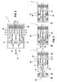
- Fig. 2 to 9 show a first embodiment in which the Anpressfedervoropathy 9 is arranged directly on the connector housing 19.
- 10 to 15 a second embodiment is shown in which the Anpressfedervortechnisch 9 is arranged directly on the contact carrier 5 and is designed to be movable with respect to this.
- Fig. 2 shows a plug 1, in contrast to Fig. 1 a collar-shaped connector housing 19, on which the Anpressfedervorraum 9 is arranged.
- the contact carrier 5 is made in two parts.
- the contact carrier halves are rotatably connected by means of a hinge 37.
- movable elements 21 can be provided, which can be deflected in a direction perpendicular to the plug-in direction 11 and a force exerted by the Anpressfedervortechnisch 9 force can be transmitted to the contact elements 7.
- the Anpressfedervortechnisch 9 has a power transmission area 17 which is arranged perpendicular to the insertion direction 11 and can cooperate with an interface or an actuating element 33 on the circuit board 3.
- the plug-in process is in Fig. 3 shown.
- the pressure spring device 9 deforms and converts the applied force into an orthogonal force. This provides as contact normal force 15 ( Fig. 3B
- the pressure spring device 9 can act directly on the contact carrier 5 or on the movable elements 21 arranged thereon.
- Fig. 4 an alternative embodiment of the Anpressfedervoriques 9 and the Anpressvorgangs is shown. In this case, a portion of the Anpressfedervoriques 9, for example, is not parallel to the contact carriers 5 and contact elements 7 but is inclined relative to this. In this way, the conversion of the force acting on the power transmission area 17 into a contact normal force can be promoted.
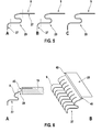
- the Anpressfedervorraum may consist of several pressure springs, each having a first region 27 and a second region 29.
- the first region 27 can connect all pressure springs with each other.
- the second area can be designed individually or separately for each pressure spring.
- the pressure spring has a second area 29, which is surrounded by a first region 27. That is, the S-shaped area is made individually for each contact element 7.
- the pressure spring is comb-like. That is, the first region 27 connects the individual pressure springs of the Anpressfedervortechnisch 9 with each other. In the second region 29, these are carried out separately.
- a compression spring is shown, which is completely individual, ie executed without connection to the adjacent pressure springs.
- Fig. 6 is another alternative embodiment of the Anpressfedervorides 9 with a contact surface 45, also referred to as a bent, shown.
- the contact surface 45 is designed to be optionally pressed flat against the plug housing 19 when a force 13 is exerted in the insertion direction on the Anpressfedervorides 9.
- the contact surface 45 can serve to stiffen the Anpressfedervorides 9 and prevent sagging. Further, the contact surface 45 can serve as a stop or travel limit for the Anpressfedervorides 9.
- the contact surface 45 is arranged in the second integral region 29 of the Anpressfedervortechnik 9 and may for example include a 90 ° -Abwinkelung the Anpressfedervortechnik 9.
- Fig. 6A shows a cross section and Fig. 6B a perspective view of the Anpressfedervorides 9. Also in Fig. 12A a contact surface 45 is shown.
- Fig. 7 shows an embodiment of the plug 1 with a recess 23 in the Anpressfedervorraum 9, in particular on the power transmission area 17.
- This is designed such that a disassembly tool 25 can be inserted through the recess 23 in the contact carrier 5, without the contact elements 7 or to damage the movable elements 21. This can be achieved, for example, by the positioning and by the dimensions of the recess 23. Due to the spacing of the power transmission region 17 from the contact carrier 5 in the non-assembled state of the plug 1, a spacer function is fulfilled by the pressure spring device 9.
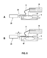
- FIG. 8 a further embodiment of the Anpressfedervorraum 9 is shown with a recess 25.
- the Anpressfedervoriques 9 offers the possibility to detect a not correctly located in position contact element 7. This can about one Position inquiry of the movable element 21 happen.
- Fig. 8A is the contact element 7 correctly positioned in the contact carrier 5, so that the disassembly tool 25 can be inserted through the recess 23 to a first penetration depth in the contact carrier 5.
- the dismantling tool 25 or another checking tool abuts the movable element 21 at the collision point designated 47 and can only penetrate into the contact carrier up to a second penetration depth.
- the second penetration depth is smaller by an amount A than the first penetration depth. Due to this difference, an incorrect positioning of the contact element 7 can be detected.
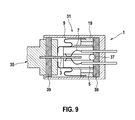
- Fig. 9 an alternative embodiment of the connector 31 is shown.
- the contact elements 7 in Fig. 9 designed as contact springs.
- no movable elements 21 are provided.
- the contact normal force 15 can be transmitted from the contact pressure spring device 9 directly or completely integrally to the contact carriers 5.
- the printed circuit board 3 is guided through a sealing mat 39 on the control unit side.
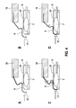
- a plug 1 according to the second embodiment is shown.
- the Anpressfedervoruze 9 is mounted directly on the contact carrier 5 and designed slidably with respect to this.
- This embodiment allows a contact assembly without force by the Anpressfedervorraum 9.
- Fig. 10A is the Anpressfedervortechnik 9 in a loading position, so that the movable elements 21 are not fixed in position and can escape during insertion of contact elements 7 in the contact carrier 5 to the outside.
- Fig. 10B For example, after loading the contact carrier 5 with contact elements 7, the movable elements 21 are manually brought into a locking position. Subsequently, as in 10C and 10D 9, the pressing spring device 9 is shifted to a locking position, so that the movable elements 21 are fixed.
- corresponding locking points can be provided on the contact carrier.
- the Anpressfedervoriques 9 provide the required power assistance for the contact production.
- Fig. 11A shown in the embodiment of the Anpressfedervortechnik 9 according to the second embodiment a force on the Anpressfedervortechnisch 9 take place only towards the end of the plug-in.
- the halves of the contact carrier 5 can open or rotate about the hinge 37, so that damage by edges of the circuit board 3 or land edges on the contact element 7 can be avoided.
- Fig. 11B shows the connector 31 in the mated position.
- the Anpressfedervortechnische 9 By a deformation of the Anpressfedervoriques 9 a contact normal force 15 is exerted on the contact elements.
- the Anpressfedervoriques 9 is also designed so that by applying force to the contact spring end 43 no moment forms, which counteracts a closure of both contact carrier halves.
- Fig. 12 shows in analogy to Fig. 5 possible embodiments of the Anpressfedervoriques 9 according to the second embodiment.
- pressure spring is connected in the first region 27 with the adjacent pressure springs and running in the second region 29 comb-like.
- the pressure spring is designed separately from the adjacent springs.
- Fig. 12C shows two pressure springs, each touching one of the two halves of the contact carrier 5. These pressure springs are connected to one another and can furthermore have first regions 27 and second regions 29.
- Fig. 13 is similar to Fig. 7 the possibility of disassembly of the contact elements 7 by a recess 23 by means of a disassembly tool 25 shown.
- the Anpressfedervoriques 9 fulfills example, in the placement position a spacer function, since it specifies a distance between the contact carrier 5 and the disassembly tool 25.
- Fig. 8 also the function of detecting an incorrect positioning of a contact element 7 to be implemented.
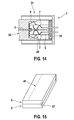
- Fig. 14 shows a connector 31 according to the second embodiment, in the similar to Fig. 9 the contact elements 7 are designed as spring contacts. In this case, the Anpressfedervoriques 9 completely integrally act on the contact carrier 5.
- the contact force or contact normal force 15 can be introduced along a contact line 43 via the contact points or via the individual contact elements 7 on the contact carrier 5. This is schematically in Fig. 15 shown. A bending of the contact carrier 5 due to a punctual introduction of the contact pressure or the contact normal force 15 can be avoided in this way.
Landscapes
- Coupling Device And Connection With Printed Circuit (AREA)
Applications Claiming Priority (1)
| Application Number | Priority Date | Filing Date | Title |
|---|---|---|---|
| DE102011081632A DE102011081632A1 (de) | 2011-08-26 | 2011-08-26 | Stecker mit Anpressfedervorrichtung zur elektrischen Direktkontaktierung einer Leiterplatte |
Publications (3)
| Publication Number | Publication Date |
|---|---|
| EP2562885A2 true EP2562885A2 (fr) | 2013-02-27 |
| EP2562885A3 EP2562885A3 (fr) | 2013-03-27 |
| EP2562885B1 EP2562885B1 (fr) | 2020-02-12 |
Family
ID=46507914
Family Applications (1)
| Application Number | Title | Priority Date | Filing Date |
|---|---|---|---|
| EP12175655.5A Active EP2562885B1 (fr) | 2011-08-26 | 2012-07-10 | Prise avec dispositif de ressort de pression pour le contact électrique direct d'une plaquette |
Country Status (2)
| Country | Link |
|---|---|
| EP (1) | EP2562885B1 (fr) |
| DE (1) | DE102011081632A1 (fr) |
Families Citing this family (1)
| Publication number | Priority date | Publication date | Assignee | Title |
|---|---|---|---|---|
| DE102014106471B4 (de) | 2014-05-08 | 2023-09-21 | Ke Elektronik Gmbh | Steckverbinder mit niedriger Steck- und hoher Kontaktnormalkraft |
Family Cites Families (6)
| Publication number | Priority date | Publication date | Assignee | Title |
|---|---|---|---|---|
| US4904197A (en) * | 1989-01-13 | 1990-02-27 | Itt Corporation | High density zif edge card connector |
| US5427533A (en) * | 1993-11-02 | 1995-06-27 | Northrop Grumman Corporation | Zero insertion force connector |
| DE10203150A1 (de) * | 2002-01-28 | 2003-07-31 | Harting Electro Optics Gmbh & | Steckverbinder mit verschiebbaren Kontaktelementen |
| DE102005063239A1 (de) * | 2005-12-20 | 2007-06-21 | Robert Bosch Gmbh | Kontaktierungssteckverbindung |
| JP2009259544A (ja) * | 2008-04-15 | 2009-11-05 | Fujitsu Ltd | コネクタ |
| JP4948574B2 (ja) * | 2009-07-24 | 2012-06-06 | 株式会社デンソー | カードエッジコネクタ及びその組付方法 |
-
2011
- 2011-08-26 DE DE102011081632A patent/DE102011081632A1/de not_active Withdrawn
-
2012
- 2012-07-10 EP EP12175655.5A patent/EP2562885B1/fr active Active
Non-Patent Citations (1)
| Title |
|---|
| None |
Also Published As
| Publication number | Publication date |
|---|---|
| EP2562885A3 (fr) | 2013-03-27 |
| EP2562885B1 (fr) | 2020-02-12 |
| DE102011081632A1 (de) | 2013-02-28 |
Similar Documents
| Publication | Publication Date | Title |
|---|---|---|
| EP2351161B1 (fr) | Système de connexion électrique enfichable | |
| DE112017001349T5 (de) | Verbindersystem mit Verbinderpositionsgewährleistung | |
| EP1901402A1 (fr) | Connecteur solaire doté de moyens d'encliquetage améliorés | |
| DE102013106117B4 (de) | Steckverbinderanordnung und Steckverbindungssystem | |
| EP3021421A1 (fr) | Dispositif de raccordement pour cable multiconducteur | |
| EP1730819B1 (fr) | Partie de connexion electrique par enfichage a force d'insertion nulle | |
| EP2545614B1 (fr) | Connecteur | |
| EP3076188B1 (fr) | Contacteur de test, procede et utilisation | |
| EP4430707A1 (fr) | Appareil de support de contact, dispositif de connexion, actionneur, insert de connecteur enfichable et procédé d'installation, et système de connexion de câble | |
| EP2942839B1 (fr) | Connecteur à fiches à faible force de couplage et à haute force normale de contact | |
| WO2013034443A1 (fr) | Connecteur électrique pourvu d'une protection de contact | |
| EP2562885B1 (fr) | Prise avec dispositif de ressort de pression pour le contact électrique direct d'une plaquette | |
| DE112018005146B4 (de) | Elektrischer verbinderkörper vom hebeltyp und zugehörige elektrische verbinderanordnung | |
| EP2012392B1 (fr) | Douille de maintien sécurisée améliorée d'un connecteur à fiches | |
| EP2026416B1 (fr) | Dispositif de réception de câble et système de contact | |
| EP3066723A1 (fr) | Câble d'essai ainsi qu'adaptateur de prise pour un câble d'essai | |
| EP3123566B1 (fr) | Douille de contact pour prise électrique | |
| EP2587595B1 (fr) | Connexion à fiche et procédé d'actionnement d'une connexion à fiche pour applications haute tension | |
| EP2200127B1 (fr) | Agencement de connecteur à fiches | |
| DE202011103484U1 (de) | Kontaktelement für eine elektrische Steckverbindervorrichtung | |
| EP2093842B1 (fr) | Boîtier pour câble, système de connecteur, procédé et utilisation | |
| WO2013087272A1 (fr) | Dispositif électrique enfichable permettant de réduire l'effort nécessaire à l'enfichage. | |
| EP2541689A1 (fr) | Prise avec une multitude de broches allongées et au moins une broche conductrice de masse en avance de phase | |
| DE102013206956B4 (de) | Schirmverbindung für Hochstromschnittstellen | |
| DE102024102096A1 (de) | Vorrichtung, Steckverbinder und Verfahren zur Schirmkontaktierung |
Legal Events
| Date | Code | Title | Description |
|---|---|---|---|
| PUAL | Search report despatched |
Free format text: ORIGINAL CODE: 0009013 |
|
| PUAI | Public reference made under article 153(3) epc to a published international application that has entered the european phase |
Free format text: ORIGINAL CODE: 0009012 |
|
| AK | Designated contracting states |
Kind code of ref document: A2 Designated state(s): AL AT BE BG CH CY CZ DE DK EE ES FI FR GB GR HR HU IE IS IT LI LT LU LV MC MK MT NL NO PL PT RO RS SE SI SK SM TR |
|
| AX | Request for extension of the european patent |
Extension state: BA ME |
|
| AK | Designated contracting states |
Kind code of ref document: A3 Designated state(s): AL AT BE BG CH CY CZ DE DK EE ES FI FR GB GR HR HU IE IS IT LI LT LU LV MC MK MT NL NO PL PT RO RS SE SI SK SM TR |
|
| AX | Request for extension of the european patent |
Extension state: BA ME |
|
| RIC1 | Information provided on ipc code assigned before grant |
Ipc: H01R 12/87 20110101ALI20130220BHEP Ipc: H01R 13/426 20060101AFI20130220BHEP Ipc: H01R 12/72 20110101ALI20130220BHEP |
|
| 17P | Request for examination filed |
Effective date: 20130927 |
|
| RBV | Designated contracting states (corrected) |
Designated state(s): AL AT BE BG CH CY CZ DE DK EE ES FI FR GB GR HR HU IE IS IT LI LT LU LV MC MK MT NL NO PL PT RO RS SE SI SK SM TR |
|
| STAA | Information on the status of an ep patent application or granted ep patent |
Free format text: STATUS: EXAMINATION IS IN PROGRESS |
|
| 17Q | First examination report despatched |
Effective date: 20180621 |
|
| GRAP | Despatch of communication of intention to grant a patent |
Free format text: ORIGINAL CODE: EPIDOSNIGR1 |
|
| STAA | Information on the status of an ep patent application or granted ep patent |
Free format text: STATUS: GRANT OF PATENT IS INTENDED |
|
| INTG | Intention to grant announced |
Effective date: 20190920 |
|
| GRAS | Grant fee paid |
Free format text: ORIGINAL CODE: EPIDOSNIGR3 |
|
| GRAA | (expected) grant |
Free format text: ORIGINAL CODE: 0009210 |
|
| STAA | Information on the status of an ep patent application or granted ep patent |
Free format text: STATUS: THE PATENT HAS BEEN GRANTED |
|
| AK | Designated contracting states |
Kind code of ref document: B1 Designated state(s): AL AT BE BG CH CY CZ DE DK EE ES FI FR GB GR HR HU IE IS IT LI LT LU LV MC MK MT NL NO PL PT RO RS SE SI SK SM TR |
|
| REG | Reference to a national code |
Ref country code: GB Ref legal event code: FG4D Free format text: NOT ENGLISH |
|
| REG | Reference to a national code |
Ref country code: CH Ref legal event code: EP |
|
| REG | Reference to a national code |
Ref country code: AT Ref legal event code: REF Ref document number: 1233337 Country of ref document: AT Kind code of ref document: T Effective date: 20200215 |
|
| REG | Reference to a national code |
Ref country code: DE Ref legal event code: R096 Ref document number: 502012015756 Country of ref document: DE |
|
| REG | Reference to a national code |
Ref country code: IE Ref legal event code: FG4D Free format text: LANGUAGE OF EP DOCUMENT: GERMAN |
|
| RAP2 | Party data changed (patent owner data changed or rights of a patent transferred) |
Owner name: ROBERT BOSCH GMBH |
|
| PG25 | Lapsed in a contracting state [announced via postgrant information from national office to epo] |
Ref country code: NO Free format text: LAPSE BECAUSE OF FAILURE TO SUBMIT A TRANSLATION OF THE DESCRIPTION OR TO PAY THE FEE WITHIN THE PRESCRIBED TIME-LIMIT Effective date: 20200512 Ref country code: FI Free format text: LAPSE BECAUSE OF FAILURE TO SUBMIT A TRANSLATION OF THE DESCRIPTION OR TO PAY THE FEE WITHIN THE PRESCRIBED TIME-LIMIT Effective date: 20200212 Ref country code: RS Free format text: LAPSE BECAUSE OF FAILURE TO SUBMIT A TRANSLATION OF THE DESCRIPTION OR TO PAY THE FEE WITHIN THE PRESCRIBED TIME-LIMIT Effective date: 20200212 |
|
| REG | Reference to a national code |
Ref country code: LT Ref legal event code: MG4D |
|
| REG | Reference to a national code |
Ref country code: NL Ref legal event code: MP Effective date: 20200212 |
|
| PG25 | Lapsed in a contracting state [announced via postgrant information from national office to epo] |
Ref country code: BG Free format text: LAPSE BECAUSE OF FAILURE TO SUBMIT A TRANSLATION OF THE DESCRIPTION OR TO PAY THE FEE WITHIN THE PRESCRIBED TIME-LIMIT Effective date: 20200512 Ref country code: GR Free format text: LAPSE BECAUSE OF FAILURE TO SUBMIT A TRANSLATION OF THE DESCRIPTION OR TO PAY THE FEE WITHIN THE PRESCRIBED TIME-LIMIT Effective date: 20200513 Ref country code: IS Free format text: LAPSE BECAUSE OF FAILURE TO SUBMIT A TRANSLATION OF THE DESCRIPTION OR TO PAY THE FEE WITHIN THE PRESCRIBED TIME-LIMIT Effective date: 20200612 Ref country code: SE Free format text: LAPSE BECAUSE OF FAILURE TO SUBMIT A TRANSLATION OF THE DESCRIPTION OR TO PAY THE FEE WITHIN THE PRESCRIBED TIME-LIMIT Effective date: 20200212 Ref country code: LV Free format text: LAPSE BECAUSE OF FAILURE TO SUBMIT A TRANSLATION OF THE DESCRIPTION OR TO PAY THE FEE WITHIN THE PRESCRIBED TIME-LIMIT Effective date: 20200212 Ref country code: HR Free format text: LAPSE BECAUSE OF FAILURE TO SUBMIT A TRANSLATION OF THE DESCRIPTION OR TO PAY THE FEE WITHIN THE PRESCRIBED TIME-LIMIT Effective date: 20200212 |
|
| PG25 | Lapsed in a contracting state [announced via postgrant information from national office to epo] |
Ref country code: NL Free format text: LAPSE BECAUSE OF FAILURE TO SUBMIT A TRANSLATION OF THE DESCRIPTION OR TO PAY THE FEE WITHIN THE PRESCRIBED TIME-LIMIT Effective date: 20200212 |
|
| PG25 | Lapsed in a contracting state [announced via postgrant information from national office to epo] |
Ref country code: ES Free format text: LAPSE BECAUSE OF FAILURE TO SUBMIT A TRANSLATION OF THE DESCRIPTION OR TO PAY THE FEE WITHIN THE PRESCRIBED TIME-LIMIT Effective date: 20200212 Ref country code: DK Free format text: LAPSE BECAUSE OF FAILURE TO SUBMIT A TRANSLATION OF THE DESCRIPTION OR TO PAY THE FEE WITHIN THE PRESCRIBED TIME-LIMIT Effective date: 20200212 Ref country code: SK Free format text: LAPSE BECAUSE OF FAILURE TO SUBMIT A TRANSLATION OF THE DESCRIPTION OR TO PAY THE FEE WITHIN THE PRESCRIBED TIME-LIMIT Effective date: 20200212 Ref country code: EE Free format text: LAPSE BECAUSE OF FAILURE TO SUBMIT A TRANSLATION OF THE DESCRIPTION OR TO PAY THE FEE WITHIN THE PRESCRIBED TIME-LIMIT Effective date: 20200212 Ref country code: SM Free format text: LAPSE BECAUSE OF FAILURE TO SUBMIT A TRANSLATION OF THE DESCRIPTION OR TO PAY THE FEE WITHIN THE PRESCRIBED TIME-LIMIT Effective date: 20200212 Ref country code: PT Free format text: LAPSE BECAUSE OF FAILURE TO SUBMIT A TRANSLATION OF THE DESCRIPTION OR TO PAY THE FEE WITHIN THE PRESCRIBED TIME-LIMIT Effective date: 20200705 Ref country code: LT Free format text: LAPSE BECAUSE OF FAILURE TO SUBMIT A TRANSLATION OF THE DESCRIPTION OR TO PAY THE FEE WITHIN THE PRESCRIBED TIME-LIMIT Effective date: 20200212 Ref country code: RO Free format text: LAPSE BECAUSE OF FAILURE TO SUBMIT A TRANSLATION OF THE DESCRIPTION OR TO PAY THE FEE WITHIN THE PRESCRIBED TIME-LIMIT Effective date: 20200212 Ref country code: CZ Free format text: LAPSE BECAUSE OF FAILURE TO SUBMIT A TRANSLATION OF THE DESCRIPTION OR TO PAY THE FEE WITHIN THE PRESCRIBED TIME-LIMIT Effective date: 20200212 |
|
| PGFP | Annual fee paid to national office [announced via postgrant information from national office to epo] |
Ref country code: GB Payment date: 20200724 Year of fee payment: 9 Ref country code: FR Payment date: 20200727 Year of fee payment: 9 |
|
| REG | Reference to a national code |
Ref country code: DE Ref legal event code: R097 Ref document number: 502012015756 Country of ref document: DE |
|
| PGFP | Annual fee paid to national office [announced via postgrant information from national office to epo] |
Ref country code: IT Payment date: 20200731 Year of fee payment: 9 |
|
| PLBE | No opposition filed within time limit |
Free format text: ORIGINAL CODE: 0009261 |
|
| STAA | Information on the status of an ep patent application or granted ep patent |
Free format text: STATUS: NO OPPOSITION FILED WITHIN TIME LIMIT |
|
| 26N | No opposition filed |
Effective date: 20201113 |
|
| PG25 | Lapsed in a contracting state [announced via postgrant information from national office to epo] |
Ref country code: PL Free format text: LAPSE BECAUSE OF FAILURE TO SUBMIT A TRANSLATION OF THE DESCRIPTION OR TO PAY THE FEE WITHIN THE PRESCRIBED TIME-LIMIT Effective date: 20200212 Ref country code: SI Free format text: LAPSE BECAUSE OF FAILURE TO SUBMIT A TRANSLATION OF THE DESCRIPTION OR TO PAY THE FEE WITHIN THE PRESCRIBED TIME-LIMIT Effective date: 20200212 Ref country code: MC Free format text: LAPSE BECAUSE OF FAILURE TO SUBMIT A TRANSLATION OF THE DESCRIPTION OR TO PAY THE FEE WITHIN THE PRESCRIBED TIME-LIMIT Effective date: 20200212 |
|
| REG | Reference to a national code |
Ref country code: CH Ref legal event code: PL |
|
| REG | Reference to a national code |
Ref country code: BE Ref legal event code: MM Effective date: 20200731 |
|
| PG25 | Lapsed in a contracting state [announced via postgrant information from national office to epo] |
Ref country code: LU Free format text: LAPSE BECAUSE OF NON-PAYMENT OF DUE FEES Effective date: 20200710 Ref country code: LI Free format text: LAPSE BECAUSE OF NON-PAYMENT OF DUE FEES Effective date: 20200731 Ref country code: CH Free format text: LAPSE BECAUSE OF NON-PAYMENT OF DUE FEES Effective date: 20200731 |
|
| PG25 | Lapsed in a contracting state [announced via postgrant information from national office to epo] |
Ref country code: BE Free format text: LAPSE BECAUSE OF NON-PAYMENT OF DUE FEES Effective date: 20200731 |
|
| PG25 | Lapsed in a contracting state [announced via postgrant information from national office to epo] |
Ref country code: IE Free format text: LAPSE BECAUSE OF NON-PAYMENT OF DUE FEES Effective date: 20200710 |
|
| REG | Reference to a national code |
Ref country code: AT Ref legal event code: MM01 Ref document number: 1233337 Country of ref document: AT Kind code of ref document: T Effective date: 20200710 |
|
| PG25 | Lapsed in a contracting state [announced via postgrant information from national office to epo] |
Ref country code: AT Free format text: LAPSE BECAUSE OF NON-PAYMENT OF DUE FEES Effective date: 20200710 |
|
| GBPC | Gb: european patent ceased through non-payment of renewal fee |
Effective date: 20210710 |
|
| PG25 | Lapsed in a contracting state [announced via postgrant information from national office to epo] |
Ref country code: GB Free format text: LAPSE BECAUSE OF NON-PAYMENT OF DUE FEES Effective date: 20210710 |
|
| PG25 | Lapsed in a contracting state [announced via postgrant information from national office to epo] |
Ref country code: TR Free format text: LAPSE BECAUSE OF FAILURE TO SUBMIT A TRANSLATION OF THE DESCRIPTION OR TO PAY THE FEE WITHIN THE PRESCRIBED TIME-LIMIT Effective date: 20200212 Ref country code: MT Free format text: LAPSE BECAUSE OF FAILURE TO SUBMIT A TRANSLATION OF THE DESCRIPTION OR TO PAY THE FEE WITHIN THE PRESCRIBED TIME-LIMIT Effective date: 20200212 Ref country code: FR Free format text: LAPSE BECAUSE OF NON-PAYMENT OF DUE FEES Effective date: 20210731 Ref country code: CY Free format text: LAPSE BECAUSE OF FAILURE TO SUBMIT A TRANSLATION OF THE DESCRIPTION OR TO PAY THE FEE WITHIN THE PRESCRIBED TIME-LIMIT Effective date: 20200212 |
|
| PG25 | Lapsed in a contracting state [announced via postgrant information from national office to epo] |
Ref country code: MK Free format text: LAPSE BECAUSE OF FAILURE TO SUBMIT A TRANSLATION OF THE DESCRIPTION OR TO PAY THE FEE WITHIN THE PRESCRIBED TIME-LIMIT Effective date: 20200212 Ref country code: AL Free format text: LAPSE BECAUSE OF FAILURE TO SUBMIT A TRANSLATION OF THE DESCRIPTION OR TO PAY THE FEE WITHIN THE PRESCRIBED TIME-LIMIT Effective date: 20200212 |
|
| PG25 | Lapsed in a contracting state [announced via postgrant information from national office to epo] |
Ref country code: IT Free format text: LAPSE BECAUSE OF NON-PAYMENT OF DUE FEES Effective date: 20210710 |
|
| PGFP | Annual fee paid to national office [announced via postgrant information from national office to epo] |
Ref country code: DE Payment date: 20220927 Year of fee payment: 11 |
|
| REG | Reference to a national code |
Ref country code: DE Ref legal event code: R119 Ref document number: 502012015756 Country of ref document: DE |
|
| PG25 | Lapsed in a contracting state [announced via postgrant information from national office to epo] |
Ref country code: DE Free format text: LAPSE BECAUSE OF NON-PAYMENT OF DUE FEES Effective date: 20240201 |