EP2564183B1 - Procédé de détermination de paramètres de matériau d'un substrat semi-conducteur dopé par la mesure du rayonnement photoluminescent - Google Patents
Procédé de détermination de paramètres de matériau d'un substrat semi-conducteur dopé par la mesure du rayonnement photoluminescent Download PDFInfo
- Publication number
- EP2564183B1 EP2564183B1 EP11715660.4A EP11715660A EP2564183B1 EP 2564183 B1 EP2564183 B1 EP 2564183B1 EP 11715660 A EP11715660 A EP 11715660A EP 2564183 B1 EP2564183 B1 EP 2564183B1
- Authority
- EP
- European Patent Office
- Prior art keywords
- semiconductor substrate
- radiation
- intensity
- excitation
- measurement
- Prior art date
- Legal status (The legal status is an assumption and is not a legal conclusion. Google has not performed a legal analysis and makes no representation as to the accuracy of the status listed.)
- Active
Links
Images


Classifications
-
- G—PHYSICS
- G01—MEASURING; TESTING
- G01N—INVESTIGATING OR ANALYSING MATERIALS BY DETERMINING THEIR CHEMICAL OR PHYSICAL PROPERTIES
- G01N21/00—Investigating or analysing materials by the use of optical means, i.e. using sub-millimetre waves, infrared, visible or ultraviolet light
- G01N21/62—Systems in which the material investigated is excited whereby it emits light or causes a change in wavelength of the incident light
- G01N21/63—Systems in which the material investigated is excited whereby it emits light or causes a change in wavelength of the incident light optically excited
- G01N21/64—Fluorescence; Phosphorescence
- G01N21/6408—Fluorescence; Phosphorescence with measurement of decay time, time resolved fluorescence
-
- G—PHYSICS
- G01—MEASURING; TESTING
- G01N—INVESTIGATING OR ANALYSING MATERIALS BY DETERMINING THEIR CHEMICAL OR PHYSICAL PROPERTIES
- G01N21/00—Investigating or analysing materials by the use of optical means, i.e. using sub-millimetre waves, infrared, visible or ultraviolet light
- G01N21/62—Systems in which the material investigated is excited whereby it emits light or causes a change in wavelength of the incident light
- G01N21/63—Systems in which the material investigated is excited whereby it emits light or causes a change in wavelength of the incident light optically excited
- G01N21/64—Fluorescence; Phosphorescence
- G01N21/6489—Photoluminescence of semiconductors
-
- G—PHYSICS
- G01—MEASURING; TESTING
- G01R—MEASURING ELECTRIC VARIABLES; MEASURING MAGNETIC VARIABLES
- G01R31/00—Arrangements for testing electric properties; Arrangements for locating electric faults; Arrangements for electrical testing characterised by what is being tested not provided for elsewhere
- G01R31/26—Testing of individual semiconductor devices
- G01R31/2648—Characterising semiconductor materials
-
- G—PHYSICS
- G01—MEASURING; TESTING
- G01R—MEASURING ELECTRIC VARIABLES; MEASURING MAGNETIC VARIABLES
- G01R31/00—Arrangements for testing electric properties; Arrangements for locating electric faults; Arrangements for electrical testing characterised by what is being tested not provided for elsewhere
- G01R31/26—Testing of individual semiconductor devices
- G01R31/265—Contactless testing
- G01R31/2656—Contactless testing using non-ionising electromagnetic radiation, e.g. optical radiation
Definitions
- the invention relates to a method for determining material parameters of a doped semiconductor substrate by measuring photoluminescence radiation.
- measurement methods are known in which modulated excitation radiation is applied to the semiconductor substrate, so that the generation rate G of charge carrier pairs in the semiconductor substrate caused by the excitation radiation is inhomogeneous over time and has at least one maximum.
- a periodic, sinusoidal modulation is used.
- the modulation is carried out in such a way that a quasi-static state is achieved.
- the corresponding measuring method with evaluation of the photoluminescence radiation is a quasi-static photoluminescence lifetime measurement (quasi-steady-state photoluminescence life time measurements, QSS-PL) known and for example in T. Trupke and RA Bardos, 31st IEEE PVSC, Orlando, 2005 described.
- the quantitative determination of the excess charge carrier density ⁇ n is essential for determining, for example, the effective life ⁇ of the minority charge carriers.
- doping concentration concentration of electrically active doping atoms N in the semiconductor substrate
- G (t) time-dependent generation rate
- the invention described here is therefore based on the object of creating a method for measuring minority charge carrier lifetimes that is based on photoluminescence and is independent of previously necessary assumptions about charge carrier mobilities, in particular a method that is independent of the determination of the doping concentration N which is generally required for lifetime measurements based on photoluminescence to accomplish.
- a method step A the doped semiconductor substrate is exposed to electromagnetic excitation radiation for generating luminescence radiation in the semiconductor substrate, the time profile of the intensity of the excitation radiation being modulated.
- the periodic modulation takes place in such a way that the generation rate G of charge carrier pairs in the semiconductor substrate has a maximum and a minimum due to the excitation radiation during an excitation period.
- the time course of the generation rate G (t) is determined by means of time-dependent measurement of the intensity of the excitation radiation.
- a time-resolved measurement of at least the relative intensity of the luminescence radiation emanating from a measurement area of the semiconductor substrate takes place, the time course of the intensity of the luminescence radiation ⁇ ( t ) being measured at least during an excitation period of the excitation radiation.
- At least one material parameter of the semiconductor substrate is determined as a function of the time profile G (t) of the generation rate and the time profile of the intensity of the luminescence radiation ⁇ ( t ).
- step C the effective lifetime ⁇ of the minority carriers of the semiconductor substrate at least at the maximum reached during an excitation period, excess charge carrier density ⁇ n max is determined in which the time difference between the maximum of G (t) and a corresponding thereto maximum of ⁇ ( t ) is determined.
- the invention is based on the applicant's knowledge that in the special case of an injection-independent service life, the effective service life of the semiconductor substrate can be determined in a surprisingly simple manner, provided that the above-mentioned condition of a quasi-static measurement method is met:
- the modulation of the excitation radiation leads to a corresponding modulation of the generation rate G (t) of charge carrier pairs in the semiconductor substrate.
- the luminescence radiation ⁇ (t ) measured as a function of time accordingly also has at least one maximum in terms of intensity.
- the maximum of the intensity of the luminescence radiation is, however, a little later than the maximum of the generation rate G (t).
- this time offset is determined.
- this time offset corresponds to the effective service life in the semiconductor substrate.
- the periodic modulation preferably takes place in step A in such a way that the minimum of the generation rate G is less than 50%, preferably less than 20%, in particular less than 10% of the maximum of the generation rate. This ensures a high level of accuracy in determining the service life.
- the generation rate is preferably modulated in a sinusoidal manner in step A, since this results in a comparatively simple mathematical treatment.
- the period T is preferably selected to be greater than the expected service life, in particular at least by a factor of 30, furthermore by at least a factor of 50, preferably by at least a factor of 100 larger. This ensures the existence of quasi-static measurement conditions.
- an exact determination of the service life can nevertheless be carried out on the basis of the measurement of the time offset between the maxima of generation rate and intensity of the photoluminescence radiation.
- Method steps A and B are preferably extended to the effect that the application of excitation radiation, the measurement of the generation rate, and the measurement of the intensity of the photoluminescence radiation take place at at least two slightly different maximum excitation intensities. These differ relatively preferably in the range between 5% and 25%, preferably in the range between 10% and 20%, furthermore preferably by about 15%.
- Method steps A and B are thus carried out at least twice, with the first and second embodiments differing in terms of the maximum excitation intensities.
- the calculated time offsets of the respective maxima of generation rate and photoluminescence intensity are used under the various excitation conditions.
- the material parameters are preferably determined using an iteration process.
- the lifetime associated with the maximum excess charge carrier density achieved during an excitation period is preferably determined by means of the aforementioned iteration method and preferably depending on the at least two time offsets determined under the various excitation conditions between the respective maximum of the generation rate and the intensity of the excitation radiation.
- Said iteration method is used to find the injection-dependent lifetime ⁇ ( ⁇ n ), which - inserted into the differential equation describing the charge carrier dynamics (see equation 4) - the measured time differences of the maxima of G (t) and ⁇ ( t ), respectively maps correctly.
- the iteration method for determining the service life is preferably designed as follows:
- the time shifts between the maxima of generation rate and intensity of the photoluminescence radiation measured for the two measurements, each with slightly different excitation intensities, are denoted here by ⁇ t 0, i , and the associated maximum generation rates by G 0, i.
- the index j indicates the respective iteration step
- the index i indicates the various excitation intensities.
- the ⁇ 1, i ( ⁇ n 1, i ) are then used for an approximation, preferably a linear approximation, of the injection-dependent service life ⁇ ( ⁇ n ) in the differential equation describing the charge carrier dynamics (equation 4) in order to in turn derive time shifts from its numerical solution To calculate ⁇ t 1, i.
- the number 0 ⁇ ⁇ ⁇ 1 is chosen so small that convergence is made possible. Typically 10-20 iteration steps are sufficient to achieve convergent lifetimes.
- the determination is the effective lifetime ⁇ of the semiconductor substrate in the area of the excess carrier density n ⁇ max possible.
- step C the effective service life ⁇ ( ⁇ n ) of the semiconductor substrate is determined as a function of the excess charge carrier density ⁇ n and / or the doping concentration N of the semiconductor substrate is determined.
- the determination in this preferred embodiment of the method according to the invention is based on the knowledge that if the quantitative time course of the generation rate G (t) is known, it is possible to determine the effective lifetime ⁇ as a function of the excess charge carrier density ⁇ n, ie not only for the immediate area in order to determine the excess charge carrier density ⁇ n max , and also the doping concentration N of the semiconductor substrate. In this preferred embodiment, too, no prior knowledge of the doping concentration N of the semiconductor substrate is necessary. In addition, it is possible to determine the doping concentration yourself from the measurement data.
- the periodic modulation is preferably carried out in step A in such a way that the minimum of the generation rate G is less than 15%, preferably less than 10%, in particular less than 5% of the maximum of the generation rate. This ensures a high level of accuracy in determining the doping concentration N.
- step C the description of the time course of the generation rate G (t) by means of a mathematical model, which has a first set of at least two fit parameters, and the description of the time course of the intensity of the photoluminescent radiation ⁇ ( t ) by means of a model analogous to the first mathematical model, which has a second set of at least two fit parameters.
- the determination of the fit parameters of the first set takes place as a function of the time-dependent measured intensity of the excitation radiation and the determination takes place accordingly the fit parameter of the second set as a function of the time-dependent measured intensity of the photoluminescence radiation.
- the excitation radiation is preferably modulated sinusoidally and the mathematical model for the temporal course of the generation rate and for the temporal course of the intensity of the photoluminescence radiation preferably has a sinusoidal function and a frequency and a phase position as fit parameters.
- the excess charge carrier density ⁇ n corresponds to the time-dependent generation rate retarded by the service life and multiplied by the service life.
- phase ⁇ ⁇ ( t ⁇ t 0 ⁇ 0 ) / T and the doping concentration N
- the initially still unknown factor A can be determined in equation 6, which enables ⁇ n ( t ) to be determined by solving equation 6.
- the time-dependent excess charge carrier density can in turn be inserted into the continuity equation (equation 4) and this (since G (t) is known) can be resolved according to the lifetime.
- the service life can thus be determined as a function of the excess charge carrier density.
- the modulation of the excitation radiation is therefore preferably selected - if the orders of magnitude of service life and doping concentration are known - such that the excess charge carrier density at maximum generation corresponds approximately to the doping concentration to be expected.
- the quantitative determination of the doping concentration N and / or the effective lifetime of the minority charge carriers ⁇ ( ⁇ n ) takes place as a function of the excess charge carrier density ⁇ n by performing method steps A and B under two very different measurement conditions:
- a first measurement condition is selected such that low injection conditions exist in the semiconductor substrate, and a second measurement condition is selected such that high injection conditions exist.
- Low injection conditions mean that the product of the maximum generation rate Go and the effective lifetime of the minority charge carriers is very small compared to the doping concentration of the semiconductor substrate.
- high injection conditions exist when the product of the maximum generation rate and the effective service life is approximately in the range of the doping concentration of the semiconductor substrate. Quasi-static measurements under low and high injection conditions are known per se, and corresponding measurement setups and parameters for generating these injection conditions are also known to the person skilled in the art.
- the time course of the generation rate is determined quantitatively. In the case of the time course of the intensity of the photoluminescence radiation, a determination in relative units is again sufficient.
- the doping concentration N of the semiconductor substrate is determined as a function of the aforementioned variables.
- the doping concentration N can be determined from equation 11 when measuring the intensity of the photoluminescence radiation ⁇ high ( t).
- An injection-dependent service life can then be determined in accordance with the procedure already described using the continuity equation (equation 4).
- the quantitative determination of the time-dependent course of the generation rate G (t) is preferably carried out as follows:
- the current density of the excitation radiation jo can be measured.
- Averaging over the entire substrate thickness provides the necessary value for the generation rate.
- a method not claimed for determining material parameters of a doped semiconductor substrate by measuring photoluminescence radiation is based on a method of self-consistent calibration, as in FIG T. Trupke, RA Bardos, MD Abbott, “Self-Consistent Calibration of Photoluminescence and Photoconductance Lifetime Measurements", Applied Physics Letters, 87: 184102, 2005 described.
- Process steps A to C correspond to the process steps described.
- the effective lifetime of the minority charge carriers of the semiconductor substrate is determined as a function of the excess charge carrier density, ⁇ ( ⁇ n ), using a self-consistency method and, at the same time, a scaling parameter A and the doping concentration N of the semiconductor substrate.
- the time-dependent intensity of the photoluminescence radiation ⁇ ( t ) can be described as a function of the time-dependent excess charge carrier density ⁇ n ( t ), the doping concentration N and a scaling factor A.
- the scaling parameter A can be determined as follows: For an incorrect scaling factor A, a so-called hysteresis curve results when the excess charge carrier density is plotted against the effective service life. However, this is an artifact that is based on the incorrect conversion between the intensity of the photoluminescence radiation and the excess charge carrier density due to the incorrect calibration factor A. It is therefore possible to determine the scaling factor A by eliminating the stroke of the hysteresis curve and thereby determine the effective life of the minority charge carriers as a function of the excess charge carrier density from the measurement data.
- the minimization can be done by defining an error function. Every excess charge carrier density below the maximum achieved occurs twice ( up / down) in the course of an excitation period. For each value pair of doping concentration N and calibration factor A , two lifetimes ⁇ up and ⁇ down can be determined according to the continuity equation (equation 4), which must be identical if the parameters N and A are chosen correctly. Said error function contains the sum of the squares of these differences between the lifetimes ⁇ up and ⁇ down, which occur at discrete, well-defined levels of the excess charge carrier density.
- ⁇ N A. ⁇ i 2 ⁇ up ⁇ n i N A. - ⁇ down ⁇ n i N A. ⁇ up ⁇ n i N A.
- the time-resolved measurement of the intensity of the luminescence radiation ⁇ ( t ) is preferably carried out in that a large number of measured values follow one another in time the intensity of the luminescence radiation is measured.
- the measurement is preferably carried out with a clock rate in the range between 10-300 kHz, depending on the modulation period T (preferably in the range 10 Hz ⁇ T -1 ⁇ 300 Hz), which depends on the expected service life.
- the measurement of the time course of the generation rate G (t) is preferably carried out in such a way that the intensity of the excitation radiation is measured analogously to the intensity of the luminescence radiation, ie by successive measurement of a plurality of measurement points for the intensity of the excitation radiation.
- the measured intensity of the excitation radiation corresponds qualitatively to the time course of the intensity of the generation rate.
- the measurement is preferably carried out with an identical clock frequency for measuring the luminescence radiation.
- the quantitative time course of the generation rate G (t) is preferably determined in the manner already described above.
- the excitation radiation is modulated periodically and preferably sinusoidally.
- the intensity of the excitation radiation and / or the intensity of the photoluminescence radiation is preferably measured over a large number of periods, and the measured values are then averaged.
- the averaging is preferably carried out over measured values of at least 100, preferably at least 300, particularly preferably at least 500 periods in order to achieve a sufficiently high signal-to-noise ratio after averaging the measured values.
- the excitation radiation is preferably generated in a manner known per se by means of a modulatable light source. Lasers are particularly suitable for this, and the use of LED light sources is also within the scope of the invention.
- the wavelength of the excitation radiation is preferably above the band edge of the semiconductor substrate to be measured, or the spectrum of the excitation radiation is preferably at least substantially above this band edge.
- the method according to the invention is particularly suitable for determining material parameters in silicon semiconductor substrates.
- the The wavelength or the center of gravity of the spectrum of the excitation radiation is therefore below 1000 nm, preferably below 900 nm.
- wavelengths between 790 nm and 880 nm are suitable for carrying out the method according to the invention.
- the method is preferably carried out using a measurement setup known per se from the QSS-PL methods.
- the excitation radiation is preferably directed from the radiation source, such as a laser, via a beam splitter onto the semiconductor substrate, part of the excitation radiation being directed via the beam splitter to a detection unit for measuring the time profile of the intensity of the excitation radiation. Diodes are particularly suitable as the detection unit.
- the beam splitter is preferably arranged and designed in such a way that only a small part of the excitation radiation, preferably less than 5%, preferably less than 2%, in particular less than 1% in terms of the intensity of the excitation radiation is directed onto the detection unit, so that the essential portion the intensity of the excitation radiation impinges on the semiconductor substrate to generate charge carrier pairs.
- the intensity of the photoluminescent radiation is preferably measured in a manner known per se by means of a diode.
- the semiconductor substrate itself already serves as a filter and shields the detection unit for the intensity of the photoluminescent radiation from the radiation source, so that errors due to the impact of excitation radiation on the detection unit for the intensity of the photoluminescent radiation are avoided.
- additional filters are attached in the beam path between the semiconductor substrate and the detection unit for the intensity of the photoluminescent radiation in order to mask out the excitation radiation. Such filters are known per se in photoluminescent structures.
- the radiation source and detection unit for the intensity of the photoluminescence radiation on the same side of the semiconductor substrate.
- filters in the beam path between the semiconductor substrate and the detection unit for the intensity of the photoluminescence radiation in order to block out any reflected excitation radiation.
- This arrangement is also known per se in measuring devices for measuring the photoluminescence radiation.
- the measuring range of the semiconductor substrate whose photoluminescence radiation is measured is defined by the detection unit for the intensity of the photoluminescence radiation or any optical elements (filters, lenses, diaphragms) in the beam path between the semiconductor substrate and the detection unit.
- the measuring area preferably represents only a partial area of the semiconductor substrate.
- the area of the measuring area projected onto a surface of the semiconductor substrate is typically between 0.5 cm 2 and 12 cm 2 , but it is also variable.
- important information with regard to the material quality of the semiconductor substrate can be obtained by determining the effective service life at one location on the semiconductor substrate. It is also within the scope of the invention to carry out a spatially resolved measurement of the material properties of the semiconductor substrate at several locations using raster or scanning measuring methods, for example by shifting the semiconductor substrate on an XY table.
- the periodic modulation of the excitation radiation is preferably carried out in such a way that the intensity of the excitation radiation has exactly one maximum in one period.
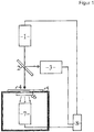
- the in Figure 1 The structure shown comprises a radiation source 1, which is designed as a diode laser with a wavelength of 880 nm.
- a beam splitter 2 is arranged in the beam path of the excitation radiation, by means of which approximately 4% of the intensity of the excitation radiation is directed onto a monitor diode 3, whereas the main part of the excitation radiation strikes a semiconductor substrate 4 in a measuring area with a size of approximately 4 cm 2.
- the semiconductor substrate 4 is a multicrystalline silicon wafer with a basic doping of ⁇ 1 ⁇ cm.
- the semiconductor substrate is arranged on a measuring table 5 on which an optical filter 6 and a PL diode 7 are arranged for measuring the intensity of the photoluminescence radiation emanating from the measuring region of the semiconductor substrate 4.
- the filter 6 is designed in such a way that radiation in the wavelength range below 970 nm is masked out.
- Radiation source 1, monitor diode 3 and PL diode 7 are connected to a control and evaluation unit 8 designed as a computer.
- the semiconductor substrate 4 is exposed to periodically modulated excitation radiation from the radiation source 1.
- the modulation is sinusoidal.
- the intensity of the excitation radiation on the semiconductor substrate is typically approximately 10 16 -10 19 cm -2 s -1 .
- the time profile of the intensity of the excitation radiation is measured qualitatively by means of the monitor diode 3, the measurement being carried out at a clock rate of typically ⁇ 10-300 kHz.
- the time profile of the intensity of the photoluminescence radiation is measured qualitatively by means of the PL diode 7, the measurement being carried out at the same clock rate as in the case of the excitation radiation.
- the measurement points belonging to curve a are the measurement results originating from the measurements of the monitor diode 3 and the measurement points belonging to the curve b are the measurement data originating from the measurements of the PL diode 7.
- the doping concentration determined from this via the ratio of the curvatures of the relative generation rate and the relative intensity of the photoluminescence radiation at their respective maxima using equation 9 is N ⁇ 1.2 ⁇ 10 16 cm -3 .
- equation 4 (as in Figure 3 shown) the service life can be determined as a function of the excess charge carrier density.
Landscapes
- Health & Medical Sciences (AREA)
- Nuclear Medicine, Radiotherapy & Molecular Imaging (AREA)
- Physics & Mathematics (AREA)
- Life Sciences & Earth Sciences (AREA)
- Chemical & Material Sciences (AREA)
- Analytical Chemistry (AREA)
- Biochemistry (AREA)
- General Health & Medical Sciences (AREA)
- General Physics & Mathematics (AREA)
- Immunology (AREA)
- Pathology (AREA)
- Testing Or Measuring Of Semiconductors Or The Like (AREA)
- Investigating, Analyzing Materials By Fluorescence Or Luminescence (AREA)
Claims (7)
- Procédé pour déterminer une durée de vie effective τ des porteurs de charge minoritaires d'un substrat semi-conducteur dopé par mesure d'un rayonnement photoluminescent dans des conditions de mesure quasi-statiques, comprenant les étapes de procédé suivantes :A appliquer au substrat semi-conducteur un rayonnement d'excitation électromagnétique pour produire un rayonnement photoluminescent dans le substrat semi-conducteur, dans lequel la courbe dans le temps de l'intensité du rayonnement d'excitation est modulée périodiquement, de telle sorte que le taux de production G de paires de porteurs de charge dans le substrat semi-conducteur (4) présente un maximum et un minimum en raison du rayonnement d'excitation pendant une période d'excitation et dans lequel au moins la courbe dans le temps relative du taux de production G(t) est déterminée à l'aide d'une mesure en fonction du temps de l'intensité du rayonnement d'excitation,B mesurer dans le temps l'intensité du rayonnement photoluminescent partant d'une zone de mesure du substrat semi-conducteur, dans lequel la courbe dans le temps de l'intensité du rayonnement photoluminescent Φ(t) est mesurée au moins pendant une période d'excitation,C déterminer la durée de vie effective τ du substrat semi-conducteur sur la base de la mesure du décalage dans le temps entre le maximum du taux de production G(t) et l'intensité du rayonnement photoluminescent Φ(t),dans lequel les étapes de procédé A et B sont réalisées par rapport à l'intensité d'excitation dans une première configuration de mesure qui est choisie de telle sorte qu'il y ait des conditions d'injection basse dans le substrat semi-conducteur, et dans l'étape C la durée de vie effective τ des porteurs de charge minoritaires est établie lors de la densité de porteurs de charge en excès maximale Δnmax atteinte pendant une période d'excitation.
- Procédé pour déterminer une durée de vie effective τ des porteurs de charge minoritaires d'un substrat semi-conducteur dopé par mesure d'un rayonnement photoluminescent dans des conditions de mesure quasi-statiques, comprenant les étapes de procédé suivantes :A appliquer au substrat semi-conducteur un rayonnement d'excitation électromagnétique pour produire un rayonnement photoluminescent dans le substrat semi-conducteur, dans lequel la courbe dans le temps de l'intensité du rayonnement d'excitation est modulée périodiquement, de telle sorte que le taux de production G de paires de porteurs de charge dans le substrat semi-conducteur (4) présente un maximum et un minimum en raison du rayonnement d'excitation pendant une période d'excitation et dans lequel au moins la courbe dans le temps du taux de production G(t) est déterminée à l'aide d'une mesure en fonction du temps de l'intensité du rayonnement d'excitation,B mesurer dans le temps l'intensité du rayonnement photoluminescent partant d'une zone de mesure du substrat semi-conducteur, dans lequel la courbe dans le temps de l'intensité du rayonnement photoluminescent Φ(t) est mesurée au moins pendant une période d'excitation,C déterminer la durée de vie effective τ des porteurs de charge minoritaires du substrat semi-conducteur par un procédé d'itération sur la base de la mesure du décalage dans le temps entre les maxima de taux de production G(t) et l'intensité du rayonnement photoluminescent Φ(t),dans lequel les étapes de procédé A et B sont réalisées par rapport à l'intensité d'excitation dans une deuxième configuration de mesure qui est choisie de telle sorte qu'il y ait des conditions d'injection élevée dans le substrat semi-conducteur, et les étapes de procédé A et B sont réalisées au moins deux fois, dans lequel les première et deuxième réalisations se différencient par les intensités d'excitation maximales, etdans l'étape C, la durée de vie effective τ du substrat semi-conducteur est établie lors de la densité de porteurs de charge en excès maximale Δnmax atteinte pendant une période d'excitation, et dans lequel les décalages dans le temps des maxima respectifs du taux de production et de l'intensité dans les différentes conditions d'excitation sont utilisés.
- Procédé selon l'une des revendications 1 ou 2 précédentes,
caractérisé
en ce que la durée de vie effective τ(Δn) du substrat semi-conducteur est déterminée en fonction de la densité de porteurs de charge en excès Δn et/ou la concentration de dopage N du substrat semi-conducteur. - Procédé selon l'une des revendications 1 ou 2 précédentes,
caractériséen ce que la courbe dans le temps du taux de production est décrite à l'aide d'un modèle mathématique qui présente un premier ensemble de respectivement au moins deux paramètres d'ajustement et la courbe dans le temps de l'intensité du rayonnement photoluminescent est décrite à l'aide d'un modèle mathématique analogue qui présente un deuxième ensemble de respectivement au moins deux paramètres d'ajustement, et les paramètres d'ajustement du premier ensemble sont déterminés en fonction des intensités du rayonnement d'excitation mesurées en fonction du temps et les paramètres d'ajustement du deuxième ensemble sont déterminés en fonction des intensités du rayonnement photoluminescent mesurées en fonction du temps, eten ce que la durée de vie effective τ du substrat semi-conducteur est déterminée en fonction de la densité de porteurs de charge en excès Δn et/ou la concentration de dopage N du substrat semi-conducteur est déterminée en fonction des premier et deuxième ensembles de paramètres d'ajustement. - Procédé selon la revendication 4,
caractérisé
en ce que la modulation du rayonnement d'excitation est sinusoïdale et le modèle mathématique pour les courbes dans le temps du taux de production et des intensités du rayonnement photoluminescent présente respectivement une fonction sinusoïdale et respectivement comme paramètres d'ajustement une fréquence et une position de phase. - Procédé selon l'une des revendications 3 à 5,
caractérisé
en ce que le rayonnement d'excitation est modulé de telle sorte que la densité de porteurs de charge en excès des porteurs de charge minoritaires dans le substrat semi-conducteur (4) avec une production maximale correspond à peu près à la concentration de dopage du substrat semi-conducteur à prévoir. - Procédé selon la revendication 1 ou 2,
caractérisé
en ce que la concentration de dopage N du substrat semi-conducteur est déterminée.
Applications Claiming Priority (2)
| Application Number | Priority Date | Filing Date | Title |
|---|---|---|---|
| DE102010019132A DE102010019132A1 (de) | 2010-04-30 | 2010-04-30 | Verfahren zur Bestimmung von Materialparametern eines dotierten Halbleitersubstrates durch Messung von Photolumineszenzstrahlung |
| PCT/EP2011/001848 WO2011134602A1 (fr) | 2010-04-30 | 2011-04-13 | Procédé de détermination de paramètres de matériau d'un substrat semi-conducteur dopé par la mesure du rayonnement photoluminescent |
Publications (2)
| Publication Number | Publication Date |
|---|---|
| EP2564183A1 EP2564183A1 (fr) | 2013-03-06 |
| EP2564183B1 true EP2564183B1 (fr) | 2021-12-01 |
Family
ID=43945292
Family Applications (1)
| Application Number | Title | Priority Date | Filing Date |
|---|---|---|---|
| EP11715660.4A Active EP2564183B1 (fr) | 2010-04-30 | 2011-04-13 | Procédé de détermination de paramètres de matériau d'un substrat semi-conducteur dopé par la mesure du rayonnement photoluminescent |
Country Status (4)
| Country | Link |
|---|---|
| US (1) | US8759793B2 (fr) |
| EP (1) | EP2564183B1 (fr) |
| DE (1) | DE102010019132A1 (fr) |
| WO (1) | WO2011134602A1 (fr) |
Families Citing this family (11)
| Publication number | Priority date | Publication date | Assignee | Title |
|---|---|---|---|---|
| US8912799B2 (en) * | 2011-11-10 | 2014-12-16 | Semiconductor Physics Laboratory Co., Ltd. | Accurate measurement of excess carrier lifetime using carrier decay method |
| DE102013202480B4 (de) | 2013-02-15 | 2019-03-07 | Fraunhofer-Gesellschaft zur Förderung der angewandten Forschung e.V. | Verfahren zur Bestimmung der tatsächlichen Ladungsträger-Lebensdauer eines Halbleitersubstrates aus einer dynamischen und differentiellen Messung der Relaxationszeit freier Ladungsträger |
| DE102013205042A1 (de) | 2013-03-21 | 2014-09-25 | Fraunhofer-Gesellschaft zur Förderung der angewandten Forschung e.V. | Verfahren und Vorrichtung zur Bestimmung von Materialparametern, insbesondere der Ladungsträgerlebensdauer eines Halbleitersubstrates durch Messung von Lumineszenzstrahlung |
| DE102013109010B4 (de) * | 2013-08-21 | 2019-03-14 | Presens - Precision Sensing Gmbh | Verfahren zur Bestimmung einer Veränderlichen einer Probe |
| JP6395206B2 (ja) * | 2014-03-25 | 2018-09-26 | 株式会社Screenホールディングス | 検査装置および検査方法 |
| DE102014005178B4 (de) | 2014-04-02 | 2018-07-26 | Friedrich-Schiller-Universität Jena | Verfahren zur ortsaufgelösten Bestimmung lokaler elektrischer Parameter eines optoelektronischen Bauelements |
| FR3073944B1 (fr) * | 2017-11-21 | 2019-12-20 | Commissariat A L'energie Atomique Et Aux Energies Alternatives | Methode de mesure par photoluminescence d'un echantillon |
| FR3098913B1 (fr) * | 2019-07-17 | 2021-08-06 | Centre Nat Rech Scient | Dispositif et méthode pour mesurer in-situ le temps de vie de porteurs minoritaires dans un matériau semi-conducteur |
| DE102019121807A1 (de) | 2019-08-13 | 2021-02-18 | Fraunhofer-Gesellschaft zur Förderung der angewandten Forschung e.V. | Verfahren und Vorrichtung zur Analyse einer Mehrfachsolarzelle mit zumindest zwei Sub-Solarzellen mittels Lumineszenzstrahlung |
| CN111366833B (zh) * | 2020-03-16 | 2022-09-09 | 深圳第三代半导体研究院 | 一种测量半导体中杂质活化能的方法 |
| CN114624501A (zh) * | 2020-12-11 | 2022-06-14 | 嘉兴阿特斯技术研究院有限公司 | 一种复合电流密度的测试方法及装置 |
Family Cites Families (10)
| Publication number | Priority date | Publication date | Assignee | Title |
|---|---|---|---|---|
| US4661770A (en) * | 1984-12-18 | 1987-04-28 | The United States Of America As Represented By The Administrator Of The National Aeronautics And Space Administration | Method and apparatus for measuring minority carrier lifetime in a direct band-gap semiconductor |
| JPH0727945B2 (ja) * | 1991-09-26 | 1995-03-29 | 信越半導体株式会社 | 半導体結晶中の深い準位密度分布の評価方法 |
| JP2975476B2 (ja) * | 1992-03-30 | 1999-11-10 | 三井金属鉱業株式会社 | 結晶内のフォトルミネッセンス計測方法及び装置 |
| US6534774B2 (en) * | 2000-09-08 | 2003-03-18 | Mitsubishi Materials Silicon Corporation | Method and apparatus for evaluating the quality of a semiconductor substrate |
| WO2005017996A1 (fr) * | 2003-03-14 | 2005-02-24 | Andreas Mandelis | Procede de radiometrie de porteurs de semi-conducteurs |
| US7919762B2 (en) * | 2006-08-01 | 2011-04-05 | Bt Imaging Pty Ltd | Determining diffusion length of minority carriers using luminescence |
| WO2008037002A1 (fr) * | 2006-09-25 | 2008-04-03 | Newsouth Innovations Pty Limited | Procédés et systèmes pour réaliser des mesures de photoluminescence avec effets de réabsorption de photons réduits |
| WO2008052237A1 (fr) * | 2006-10-30 | 2008-05-08 | Newsouth Innovations Pty Limited | Procédés et systèmes permettant de produire de manière auto-cohérente une constante d'étalonnage pour la durée de vie des porteurs de charge en excès |
| DE102008013068B4 (de) * | 2008-03-06 | 2012-06-21 | Institut Für Solarenergieforschung Gmbh | Verfahren und Vorrichtung zur ortsaufgelösten Bestimmung von Ladungsträgerlebensdauern in Halbleiterstrukturen |
| DE102008044879A1 (de) * | 2008-08-29 | 2010-03-04 | Fraunhofer-Gesellschaft zur Förderung der angewandten Forschung e.V. | Verfahren zur Bestimmung der Überschussladungsträgerlebensdauer in einer Halbleiterschicht |
-
2010
- 2010-04-30 DE DE102010019132A patent/DE102010019132A1/de not_active Ceased
-
2011
- 2011-04-13 WO PCT/EP2011/001848 patent/WO2011134602A1/fr not_active Ceased
- 2011-04-13 EP EP11715660.4A patent/EP2564183B1/fr active Active
- 2011-04-13 US US13/695,452 patent/US8759793B2/en active Active
Also Published As
| Publication number | Publication date |
|---|---|
| EP2564183A1 (fr) | 2013-03-06 |
| DE102010019132A1 (de) | 2011-11-03 |
| WO2011134602A1 (fr) | 2011-11-03 |
| US8759793B2 (en) | 2014-06-24 |
| US20130146787A1 (en) | 2013-06-13 |
Similar Documents
| Publication | Publication Date | Title |
|---|---|---|
| EP2564183B1 (fr) | Procédé de détermination de paramètres de matériau d'un substrat semi-conducteur dopé par la mesure du rayonnement photoluminescent | |
| DE69425316T2 (de) | Verfahren zur Bestimmung der Rekombinationslebendauer von Minoritäts-Ladungsträgern einer Probe aus Halbleitermaterial | |
| DE112011103163B4 (de) | Kristallqualitäts-Evaluierungsvorrichtung für Dünnfilm-Halbleiter unter Verwendung einer μ- PCD Technik | |
| DE102005040010A1 (de) | Verfahren und Vorrichtung zur Ermittlung von Produktionsfehlern in einem Halbleiterbau-element | |
| EP2433148B1 (fr) | Procédé pour déterminer spatialement la résistance série d'une structure semi-conductrice | |
| DE3116611C2 (de) | Vorrichtung zur Messung von Halbleitereigenschaften | |
| DE112016001907B4 (de) | Herstellungsverfahren und Beurteilungsverfahren für Silizium-Epiwafer | |
| DE4321548A1 (de) | Verfahren zum Erfassen und Auswerten analoger photometrischer Signale in einem Testträger-Analysesystem und Anordnung zur Durchführung des Verfahrens | |
| DE112014007063T5 (de) | Siliciumcarbid-Epitaxialwafer-Herstellungsverfahren | |
| EP2950446A1 (fr) | Procédé de détection d'un degré de salissure de panneaux pv | |
| EP2516990A1 (fr) | Analyseur de gaz infrarouge non dispersif à double faisceau et procédé pour déterminer la concentration d'un constituant gazeux à mesurer dans un mélange gazeux au moyen d'un tel analyseur de gaz | |
| DE19831216A1 (de) | Verfahren und Vorrichtung zur Bestimmung der Abhängigkeit einer ersten Meßgröße von einer zweiten Meßgröße | |
| DE102004037603B3 (de) | Regelung der UV-Strahlungsquellen einer Bewitterungsvorrichtung auf der Basis der gemittelten Strahlungsintensität | |
| DE102014119607A1 (de) | Ermittlung der Leistungsdichteverteilung eines Photovoltaikgenerators aus zeitlichen Verläufen seiner elektrischen Leistung | |
| DE102004014984B4 (de) | Verfahren zur Bestimmung des substitutionellen Kohlenstoffgehalts in poly- oder monokristallinem Silicium | |
| DE112022005169T5 (de) | Phasendifferenz-messvorrichtung, messverfahren und elektrisches gerät umfassend dieselbe | |
| WO2010022922A1 (fr) | Procédé pour la détermination de la durée de vie d’un porteur de surcharge dans une couche semi-conductrice | |
| EP0400373A2 (fr) | Procédé pour la détermination de la résolution spatiale de la longueur de diffusion de porteurs minoritaires de charge dans un corps cristallin semi-conducteur à l'aide d'une cellule électrolytique | |
| DE102008013068A1 (de) | Verfahren und Vorrichtung zur ortsaufgelösten Bestimmung von Ladungsträgerlebensdauern in Halbleiterstrukturen | |
| DE112012002507B4 (de) | Verfahren zur Bewertung von metallischen Verunreinigungen in einer Halbleiterprobe und Verfahren zur Herstellung eines Halbleitersubtrats | |
| DE10311658A1 (de) | Verfahren und Vorrichtung zum Bestimmen einer Eigenschaft einer Halbleiterprobe | |
| DE102009048155B4 (de) | Verfahren und Vorrichtung zum Bestimmen eines Dehnungsprofils in einer optischen Faser | |
| EP0400386A2 (fr) | Procédé pour déterminer la vitesse de recombination de porteurs minoritaires aux surfaces de séparation entre semi-conducteurs et autres matières | |
| DE102014005178B4 (de) | Verfahren zur ortsaufgelösten Bestimmung lokaler elektrischer Parameter eines optoelektronischen Bauelements | |
| EP2318851B1 (fr) | Procédé permettant de déterminer les propriétés de recombinaison au niveau d'une zone partielle de mesure d'un côté de mesure d'une structure semi-conductrice |
Legal Events
| Date | Code | Title | Description |
|---|---|---|---|
| PUAI | Public reference made under article 153(3) epc to a published international application that has entered the european phase |
Free format text: ORIGINAL CODE: 0009012 |
|
| 17P | Request for examination filed |
Effective date: 20121026 |
|
| AK | Designated contracting states |
Kind code of ref document: A1 Designated state(s): AL AT BE BG CH CY CZ DE DK EE ES FI FR GB GR HR HU IE IS IT LI LT LU LV MC MK MT NL NO PL PT RO RS SE SI SK SM TR |
|
| DAX | Request for extension of the european patent (deleted) | ||
| STAA | Information on the status of an ep patent application or granted ep patent |
Free format text: STATUS: EXAMINATION IS IN PROGRESS |
|
| 17Q | First examination report despatched |
Effective date: 20190225 |
|
| REG | Reference to a national code |
Ref country code: DE Ref legal event code: R079 Ref document number: 502011017271 Country of ref document: DE Free format text: PREVIOUS MAIN CLASS: G01N0021640000 Ipc: G01R0031265000 |
|
| GRAP | Despatch of communication of intention to grant a patent |
Free format text: ORIGINAL CODE: EPIDOSNIGR1 |
|
| STAA | Information on the status of an ep patent application or granted ep patent |
Free format text: STATUS: GRANT OF PATENT IS INTENDED |
|
| RIC1 | Information provided on ipc code assigned before grant |
Ipc: G01R 31/265 20060101AFI20210526BHEP Ipc: G01N 21/64 20060101ALI20210526BHEP Ipc: G01R 31/26 20200101ALI20210526BHEP |
|
| INTG | Intention to grant announced |
Effective date: 20210623 |
|
| GRAS | Grant fee paid |
Free format text: ORIGINAL CODE: EPIDOSNIGR3 |
|
| GRAA | (expected) grant |
Free format text: ORIGINAL CODE: 0009210 |
|
| STAA | Information on the status of an ep patent application or granted ep patent |
Free format text: STATUS: THE PATENT HAS BEEN GRANTED |
|
| AK | Designated contracting states |
Kind code of ref document: B1 Designated state(s): AL AT BE BG CH CY CZ DE DK EE ES FI FR GB GR HR HU IE IS IT LI LT LU LV MC MK MT NL NO PL PT RO RS SE SI SK SM TR |
|
| REG | Reference to a national code |
Ref country code: GB Ref legal event code: FG4D Free format text: NOT ENGLISH |
|
| REG | Reference to a national code |
Ref country code: AT Ref legal event code: REF Ref document number: 1452278 Country of ref document: AT Kind code of ref document: T Effective date: 20211215 Ref country code: CH Ref legal event code: EP |
|
| REG | Reference to a national code |
Ref country code: IE Ref legal event code: FG4D Free format text: LANGUAGE OF EP DOCUMENT: GERMAN |
|
| REG | Reference to a national code |
Ref country code: DE Ref legal event code: R096 Ref document number: 502011017271 Country of ref document: DE |
|
| REG | Reference to a national code |
Ref country code: LT Ref legal event code: MG9D |
|
| REG | Reference to a national code |
Ref country code: NL Ref legal event code: MP Effective date: 20211201 |
|
| RAP4 | Party data changed (patent owner data changed or rights of a patent transferred) |
Owner name: FRAUNHOFER-GESELLSCHAFT ZUR FOERDERUNG DER ANGEWANDTEN FORSCHUNG E.V. |
|
| PG25 | Lapsed in a contracting state [announced via postgrant information from national office to epo] |
Ref country code: RS Free format text: LAPSE BECAUSE OF FAILURE TO SUBMIT A TRANSLATION OF THE DESCRIPTION OR TO PAY THE FEE WITHIN THE PRESCRIBED TIME-LIMIT Effective date: 20211201 Ref country code: LT Free format text: LAPSE BECAUSE OF FAILURE TO SUBMIT A TRANSLATION OF THE DESCRIPTION OR TO PAY THE FEE WITHIN THE PRESCRIBED TIME-LIMIT Effective date: 20211201 Ref country code: FI Free format text: LAPSE BECAUSE OF FAILURE TO SUBMIT A TRANSLATION OF THE DESCRIPTION OR TO PAY THE FEE WITHIN THE PRESCRIBED TIME-LIMIT Effective date: 20211201 Ref country code: BG Free format text: LAPSE BECAUSE OF FAILURE TO SUBMIT A TRANSLATION OF THE DESCRIPTION OR TO PAY THE FEE WITHIN THE PRESCRIBED TIME-LIMIT Effective date: 20220301 |
|
| PG25 | Lapsed in a contracting state [announced via postgrant information from national office to epo] |
Ref country code: SE Free format text: LAPSE BECAUSE OF FAILURE TO SUBMIT A TRANSLATION OF THE DESCRIPTION OR TO PAY THE FEE WITHIN THE PRESCRIBED TIME-LIMIT Effective date: 20211201 Ref country code: PL Free format text: LAPSE BECAUSE OF FAILURE TO SUBMIT A TRANSLATION OF THE DESCRIPTION OR TO PAY THE FEE WITHIN THE PRESCRIBED TIME-LIMIT Effective date: 20211201 Ref country code: NO Free format text: LAPSE BECAUSE OF FAILURE TO SUBMIT A TRANSLATION OF THE DESCRIPTION OR TO PAY THE FEE WITHIN THE PRESCRIBED TIME-LIMIT Effective date: 20220301 Ref country code: LV Free format text: LAPSE BECAUSE OF FAILURE TO SUBMIT A TRANSLATION OF THE DESCRIPTION OR TO PAY THE FEE WITHIN THE PRESCRIBED TIME-LIMIT Effective date: 20211201 Ref country code: HR Free format text: LAPSE BECAUSE OF FAILURE TO SUBMIT A TRANSLATION OF THE DESCRIPTION OR TO PAY THE FEE WITHIN THE PRESCRIBED TIME-LIMIT Effective date: 20211201 Ref country code: GR Free format text: LAPSE BECAUSE OF FAILURE TO SUBMIT A TRANSLATION OF THE DESCRIPTION OR TO PAY THE FEE WITHIN THE PRESCRIBED TIME-LIMIT Effective date: 20220302 Ref country code: ES Free format text: LAPSE BECAUSE OF FAILURE TO SUBMIT A TRANSLATION OF THE DESCRIPTION OR TO PAY THE FEE WITHIN THE PRESCRIBED TIME-LIMIT Effective date: 20211201 |
|
| PG25 | Lapsed in a contracting state [announced via postgrant information from national office to epo] |
Ref country code: NL Free format text: LAPSE BECAUSE OF FAILURE TO SUBMIT A TRANSLATION OF THE DESCRIPTION OR TO PAY THE FEE WITHIN THE PRESCRIBED TIME-LIMIT Effective date: 20211201 |
|
| PG25 | Lapsed in a contracting state [announced via postgrant information from national office to epo] |
Ref country code: SM Free format text: LAPSE BECAUSE OF FAILURE TO SUBMIT A TRANSLATION OF THE DESCRIPTION OR TO PAY THE FEE WITHIN THE PRESCRIBED TIME-LIMIT Effective date: 20211201 Ref country code: SK Free format text: LAPSE BECAUSE OF FAILURE TO SUBMIT A TRANSLATION OF THE DESCRIPTION OR TO PAY THE FEE WITHIN THE PRESCRIBED TIME-LIMIT Effective date: 20211201 Ref country code: RO Free format text: LAPSE BECAUSE OF FAILURE TO SUBMIT A TRANSLATION OF THE DESCRIPTION OR TO PAY THE FEE WITHIN THE PRESCRIBED TIME-LIMIT Effective date: 20211201 Ref country code: PT Free format text: LAPSE BECAUSE OF FAILURE TO SUBMIT A TRANSLATION OF THE DESCRIPTION OR TO PAY THE FEE WITHIN THE PRESCRIBED TIME-LIMIT Effective date: 20220401 Ref country code: EE Free format text: LAPSE BECAUSE OF FAILURE TO SUBMIT A TRANSLATION OF THE DESCRIPTION OR TO PAY THE FEE WITHIN THE PRESCRIBED TIME-LIMIT Effective date: 20211201 Ref country code: CZ Free format text: LAPSE BECAUSE OF FAILURE TO SUBMIT A TRANSLATION OF THE DESCRIPTION OR TO PAY THE FEE WITHIN THE PRESCRIBED TIME-LIMIT Effective date: 20211201 |
|
| REG | Reference to a national code |
Ref country code: DE Ref legal event code: R097 Ref document number: 502011017271 Country of ref document: DE |
|
| PG25 | Lapsed in a contracting state [announced via postgrant information from national office to epo] |
Ref country code: IS Free format text: LAPSE BECAUSE OF FAILURE TO SUBMIT A TRANSLATION OF THE DESCRIPTION OR TO PAY THE FEE WITHIN THE PRESCRIBED TIME-LIMIT Effective date: 20220401 |
|
| PLBE | No opposition filed within time limit |
Free format text: ORIGINAL CODE: 0009261 |
|
| STAA | Information on the status of an ep patent application or granted ep patent |
Free format text: STATUS: NO OPPOSITION FILED WITHIN TIME LIMIT |
|
| PG25 | Lapsed in a contracting state [announced via postgrant information from national office to epo] |
Ref country code: DK Free format text: LAPSE BECAUSE OF FAILURE TO SUBMIT A TRANSLATION OF THE DESCRIPTION OR TO PAY THE FEE WITHIN THE PRESCRIBED TIME-LIMIT Effective date: 20211201 Ref country code: AL Free format text: LAPSE BECAUSE OF FAILURE TO SUBMIT A TRANSLATION OF THE DESCRIPTION OR TO PAY THE FEE WITHIN THE PRESCRIBED TIME-LIMIT Effective date: 20211201 |
|
| 26N | No opposition filed |
Effective date: 20220902 |
|
| PG25 | Lapsed in a contracting state [announced via postgrant information from national office to epo] |
Ref country code: SI Free format text: LAPSE BECAUSE OF FAILURE TO SUBMIT A TRANSLATION OF THE DESCRIPTION OR TO PAY THE FEE WITHIN THE PRESCRIBED TIME-LIMIT Effective date: 20211201 |
|
| REG | Reference to a national code |
Ref country code: CH Ref legal event code: PL |
|
| REG | Reference to a national code |
Ref country code: BE Ref legal event code: MM Effective date: 20220430 |
|
| PG25 | Lapsed in a contracting state [announced via postgrant information from national office to epo] |
Ref country code: MC Free format text: LAPSE BECAUSE OF FAILURE TO SUBMIT A TRANSLATION OF THE DESCRIPTION OR TO PAY THE FEE WITHIN THE PRESCRIBED TIME-LIMIT Effective date: 20211201 Ref country code: LU Free format text: LAPSE BECAUSE OF NON-PAYMENT OF DUE FEES Effective date: 20220413 Ref country code: LI Free format text: LAPSE BECAUSE OF NON-PAYMENT OF DUE FEES Effective date: 20220430 Ref country code: CH Free format text: LAPSE BECAUSE OF NON-PAYMENT OF DUE FEES Effective date: 20220430 |
|
| PG25 | Lapsed in a contracting state [announced via postgrant information from national office to epo] |
Ref country code: BE Free format text: LAPSE BECAUSE OF NON-PAYMENT OF DUE FEES Effective date: 20220430 |
|
| PG25 | Lapsed in a contracting state [announced via postgrant information from national office to epo] |
Ref country code: IE Free format text: LAPSE BECAUSE OF NON-PAYMENT OF DUE FEES Effective date: 20220413 |
|
| PG25 | Lapsed in a contracting state [announced via postgrant information from national office to epo] |
Ref country code: IT Free format text: LAPSE BECAUSE OF FAILURE TO SUBMIT A TRANSLATION OF THE DESCRIPTION OR TO PAY THE FEE WITHIN THE PRESCRIBED TIME-LIMIT Effective date: 20211201 |
|
| REG | Reference to a national code |
Ref country code: AT Ref legal event code: MM01 Ref document number: 1452278 Country of ref document: AT Kind code of ref document: T Effective date: 20220413 |
|
| P01 | Opt-out of the competence of the unified patent court (upc) registered |
Effective date: 20230524 |
|
| PG25 | Lapsed in a contracting state [announced via postgrant information from national office to epo] |
Ref country code: AT Free format text: LAPSE BECAUSE OF NON-PAYMENT OF DUE FEES Effective date: 20220413 |
|
| PG25 | Lapsed in a contracting state [announced via postgrant information from national office to epo] |
Ref country code: HU Free format text: LAPSE BECAUSE OF FAILURE TO SUBMIT A TRANSLATION OF THE DESCRIPTION OR TO PAY THE FEE WITHIN THE PRESCRIBED TIME-LIMIT; INVALID AB INITIO Effective date: 20110413 |
|
| PG25 | Lapsed in a contracting state [announced via postgrant information from national office to epo] |
Ref country code: MK Free format text: LAPSE BECAUSE OF FAILURE TO SUBMIT A TRANSLATION OF THE DESCRIPTION OR TO PAY THE FEE WITHIN THE PRESCRIBED TIME-LIMIT Effective date: 20211201 Ref country code: CY Free format text: LAPSE BECAUSE OF FAILURE TO SUBMIT A TRANSLATION OF THE DESCRIPTION OR TO PAY THE FEE WITHIN THE PRESCRIBED TIME-LIMIT Effective date: 20211201 |
|
| PG25 | Lapsed in a contracting state [announced via postgrant information from national office to epo] |
Ref country code: MT Free format text: LAPSE BECAUSE OF FAILURE TO SUBMIT A TRANSLATION OF THE DESCRIPTION OR TO PAY THE FEE WITHIN THE PRESCRIBED TIME-LIMIT Effective date: 20211201 |
|
| PGFP | Annual fee paid to national office [announced via postgrant information from national office to epo] |
Ref country code: DE Payment date: 20250417 Year of fee payment: 15 |
|
| PGFP | Annual fee paid to national office [announced via postgrant information from national office to epo] |
Ref country code: GB Payment date: 20250423 Year of fee payment: 15 |
|
| PGFP | Annual fee paid to national office [announced via postgrant information from national office to epo] |
Ref country code: FR Payment date: 20250422 Year of fee payment: 15 |
|
| PG25 | Lapsed in a contracting state [announced via postgrant information from national office to epo] |
Ref country code: TR Free format text: LAPSE BECAUSE OF FAILURE TO SUBMIT A TRANSLATION OF THE DESCRIPTION OR TO PAY THE FEE WITHIN THE PRESCRIBED TIME-LIMIT Effective date: 20211201 |