EP2565746A2 - Appareil électronique mobile comportant des cellules solaires - Google Patents
Appareil électronique mobile comportant des cellules solaires Download PDFInfo
- Publication number
- EP2565746A2 EP2565746A2 EP12162679A EP12162679A EP2565746A2 EP 2565746 A2 EP2565746 A2 EP 2565746A2 EP 12162679 A EP12162679 A EP 12162679A EP 12162679 A EP12162679 A EP 12162679A EP 2565746 A2 EP2565746 A2 EP 2565746A2
- Authority
- EP
- European Patent Office
- Prior art keywords
- electronic apparatus
- mobile electronic
- board
- solar cell
- cell module
- Prior art date
- Legal status (The legal status is an assumption and is not a legal conclusion. Google has not performed a legal analysis and makes no representation as to the accuracy of the status listed.)
- Granted
Links
Images




Classifications
-
- G—PHYSICS
- G06—COMPUTING OR CALCULATING; COUNTING
- G06F—ELECTRIC DIGITAL DATA PROCESSING
- G06F1/00—Details not covered by groups G06F3/00 - G06F13/00 and G06F21/00
- G06F1/26—Power supply means, e.g. regulation thereof
- G06F1/263—Arrangements for using multiple switchable power supplies, e.g. battery and AC
-
- G—PHYSICS
- G06—COMPUTING OR CALCULATING; COUNTING
- G06F—ELECTRIC DIGITAL DATA PROCESSING
- G06F1/00—Details not covered by groups G06F3/00 - G06F13/00 and G06F21/00
- G06F1/26—Power supply means, e.g. regulation thereof
-
- G—PHYSICS
- G06—COMPUTING OR CALCULATING; COUNTING
- G06F—ELECTRIC DIGITAL DATA PROCESSING
- G06F1/00—Details not covered by groups G06F3/00 - G06F13/00 and G06F21/00
- G06F1/16—Constructional details or arrangements
-
- G—PHYSICS
- G06—COMPUTING OR CALCULATING; COUNTING
- G06F—ELECTRIC DIGITAL DATA PROCESSING
- G06F1/00—Details not covered by groups G06F3/00 - G06F13/00 and G06F21/00
- G06F1/16—Constructional details or arrangements
- G06F1/1613—Constructional details or arrangements for portable computers
-
- G—PHYSICS
- G06—COMPUTING OR CALCULATING; COUNTING
- G06F—ELECTRIC DIGITAL DATA PROCESSING
- G06F1/00—Details not covered by groups G06F3/00 - G06F13/00 and G06F21/00
- G06F1/16—Constructional details or arrangements
- G06F1/1613—Constructional details or arrangements for portable computers
- G06F1/1615—Constructional details or arrangements for portable computers with several enclosures having relative motions, each enclosure supporting at least one I/O or computing function
- G06F1/1616—Constructional details or arrangements for portable computers with several enclosures having relative motions, each enclosure supporting at least one I/O or computing function with folding flat displays, e.g. laptop computers or notebooks having a clamshell configuration, with body parts pivoting to an open position around an axis parallel to the plane they define in closed position
-
- G—PHYSICS
- G06—COMPUTING OR CALCULATING; COUNTING
- G06F—ELECTRIC DIGITAL DATA PROCESSING
- G06F1/00—Details not covered by groups G06F3/00 - G06F13/00 and G06F21/00
- G06F1/16—Constructional details or arrangements
- G06F1/1613—Constructional details or arrangements for portable computers
- G06F1/1633—Constructional details or arrangements of portable computers not specific to the type of enclosures covered by groups G06F1/1615 - G06F1/1626
- G06F1/1635—Details related to the integration of battery packs and other power supplies such as fuel cells or integrated AC adapter
-
- G—PHYSICS
- G06—COMPUTING OR CALCULATING; COUNTING
- G06F—ELECTRIC DIGITAL DATA PROCESSING
- G06F1/00—Details not covered by groups G06F3/00 - G06F13/00 and G06F21/00
- G06F1/16—Constructional details or arrangements
- G06F1/1613—Constructional details or arrangements for portable computers
- G06F1/1633—Constructional details or arrangements of portable computers not specific to the type of enclosures covered by groups G06F1/1615 - G06F1/1626
- G06F1/1637—Details related to the display arrangement, including those related to the mounting of the display in the housing
-
- G—PHYSICS
- G06—COMPUTING OR CALCULATING; COUNTING
- G06F—ELECTRIC DIGITAL DATA PROCESSING
- G06F1/00—Details not covered by groups G06F3/00 - G06F13/00 and G06F21/00
- G06F1/16—Constructional details or arrangements
- G06F1/18—Packaging or power distribution
- G06F1/183—Internal mounting support structures, e.g. for supporting printed circuit boards
- G06F1/188—Mounting of power supply units
-
- G—PHYSICS
- G06—COMPUTING OR CALCULATING; COUNTING
- G06F—ELECTRIC DIGITAL DATA PROCESSING
- G06F1/00—Details not covered by groups G06F3/00 - G06F13/00 and G06F21/00
- G06F1/16—Constructional details or arrangements
- G06F1/18—Packaging or power distribution
- G06F1/189—Power distribution
-
- H—ELECTRICITY
- H02—GENERATION; CONVERSION OR DISTRIBUTION OF ELECTRIC POWER
- H02J—ELECTRIC POWER NETWORKS; CIRCUIT ARRANGEMENTS OR SYSTEMS FOR SUPPLYING OR DISTRIBUTING ELECTRIC POWER; SYSTEMS FOR STORING ELECTRIC ENERGY
- H02J7/00—Circuit arrangements for charging or discharging batteries or for supplying loads from batteries
- H02J7/34—Parallel operation in networks using both storage and other DC sources, e.g. providing buffering
- H02J7/35—Parallel operation in networks using both storage and other DC sources, e.g. providing buffering with light sensitive cells
-
- H—ELECTRICITY
- H04—ELECTRIC COMMUNICATION TECHNIQUE
- H04M—TELEPHONIC COMMUNICATION
- H04M1/00—Substation equipment, e.g. for use by subscribers
- H04M1/02—Constructional features of telephone sets
- H04M1/21—Combinations with auxiliary equipment, e.g. with clocks or memoranda pads
-
- Y—GENERAL TAGGING OF NEW TECHNOLOGICAL DEVELOPMENTS; GENERAL TAGGING OF CROSS-SECTIONAL TECHNOLOGIES SPANNING OVER SEVERAL SECTIONS OF THE IPC; TECHNICAL SUBJECTS COVERED BY FORMER USPC CROSS-REFERENCE ART COLLECTIONS [XRACs] AND DIGESTS
- Y02—TECHNOLOGIES OR APPLICATIONS FOR MITIGATION OR ADAPTATION AGAINST CLIMATE CHANGE
- Y02E—REDUCTION OF GREENHOUSE GAS [GHG] EMISSIONS, RELATED TO ENERGY GENERATION, TRANSMISSION OR DISTRIBUTION
- Y02E10/00—Energy generation through renewable energy sources
- Y02E10/50—Photovoltaic [PV] energy
Definitions
- the present invention relates to a mobile electronic apparatus. More particularly, the present invention relates to a mobile electronic apparatus which can supply electric power by using solar cells.
- solar cells are used as electrical power sources for mobile electronic apparatuses such as notebook computers, netbook computers, personal media players, mobile terminals, portable electronic books, and other similar portable electronic devices.
- mobile electronic apparatuses such as notebook computers, netbook computers, personal media players, mobile terminals, portable electronic books, and other similar portable electronic devices.
- the solar cells need to supply a constant and stable voltage to the mobile electronic apparatus.
- an output voltage of the solar cells changes according to factors such as an amount of sunlight or an irradiating circumstance of the solar cells, such as the presence of clouds in the sky, an angle of incidence of the light, and other similar factors, the solar cells need to be modified in order to provide a stable electric power source which can provide a constant output voltage.
- a converter system is used to convert unstable output voltage of the solar cells into stable voltage at a high-speed.
- a solar cell DC/DC converter may be used as the converter system of the unstable output voltage of the solar cells.
- a separate converting circuit which operates as the converter system is arranged in the mobile electronic apparatus.
- the converting circuit is arranged on a main board thereof, while the solar cells are disposed on an outside surface or on a keyboard surface of the mobile electronic apparatus.
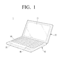
- FIG. 1 illustrates a netbook computer as an example of a mobile electronic apparatus according to the related art.
- a converting circuit 40 is disposed with or on a main board 30, both of which are disposed in a main body unit 10 of the netbook computer 1.
- a keyboard 50 is disposed on the main body unit 10.
- Solar cells (not illustrated) are disposed on a rear side of a screen portion 21 of a display unit 20, such as an LCD unit or any other similar display unit.
- the main board 30 has a separate area for receiving the converting circuit 40.
- the unstable electric power moves through a long cable from the solar cells of the display unit 20 to the main board 30 of the main body unit 10, loss of electric power is likely to occur.
- the unstable electric power may cause electronic noise so as to affect other parts of the netbook computer 1.
- the solar cells when the solar cells are disposed so as to be exposed to the outside of the mobile electronic apparatus 1, the solar cells may be damaged by an external impact or the solar cells may be contaminated by environmental contaminants.
- an aspect of the present invention is to provide a mobile electronic apparatus that can reduce output electric power loss of solar cells by arranging a converting circuit close to the solar cells.
- Another aspect of the present invention is to provide a mobile electronic apparatus that can effectively prevent Electromagnetic Interference (EMI) by transmitting stable electric power to a main body unit using an existing display cable connecting a display unit and a main board of the main body unit.
- EMI Electromagnetic Interference
- the present disclosure relates to a mobile electronic apparatus that can increase efficiency of the solar cells by disposing a fixing bracket between the display unit and the solar cells so as to secure the solar cells and to effectively release heat generated by the solar cells.
- the present invention relates to a mobile electronic apparatus having a cover capable of protecting solar cells.
- a mobile electronic apparatus includes a main body unit including a main board, a display unit disposed so as to rotate with respect to the main body unit for operating according to a control of the main board, a solar cell module disposed on a rear surface of the display unit for generating electric power by converting solar energy into electric power, and a converting circuit disposed inside the display unit for stabilizing electric power generated by the solar cell module so as to supply stable electric power.
- the display unit may include a display driving board, and the converting circuit may be formed in the display driving board.
- the converting circuit may be formed on a separate exclusive board.
- the converting circuit may be formed on a sub-board having a function different from a function of the display driving board.
- the sub-board may include a camera module board, a 3rd Generation (3G) system board, a 4th Generation (4G) system board, and an antenna board.
- 3G 3rd Generation
- 4G 4th Generation
- the mobile electronic apparatus may include a display cable connecting the display unit and the main board, wherein the electric power converted by the converting circuit may be supplied to the main board through the display cable.
- the mobile electronic apparatus may include a fixing bracket disposed between the display unit and the solar cell module so as to affix the solar cell module to the display unit.
- the fixing bracket may include a cushioning member.
- the fixing bracket may be formed of a thermally conductive material.
- the mobile electronic apparatus may include a protection cover disposed above the solar cell module, wherein the protection cover may be transparent so that sunlight can pass through the protection cover.
- the mobile electronic apparatus may include a gap maintaining member disposed between the protection cover and the solar cell module.
- the gap maintaining member may include an insulating tape.
- a mobile electronic apparatus includes a main body unit including a main board, a display unit disposed so as to rotate with respect to the main body unit for displaying data according to a control of the main board, a solar cell module disposed on a rear surface of the display unit for generating electric power by converting solar energy into electric power, a fixing bracket disposed between the display unit and the solar cell module so as to affix the solar cell module to the display unit, a protection cover disposed above the solar cell module and which is transparent so that sunlight can pass through the protection cover, and a converting circuit disposed inside the display unit for stabilizing the electric power generated by the solar cell module so as to supply stable electric power.
- FIG. 2 is a perspective view schematically illustrating a mobile electronic apparatus according to an exemplary embodiment of the present invention
- FIG. 3 is an exploded perspective view schematically illustrating a solar cell module of a display unit of a mobile electronic apparatus according to an exemplary embodiment of the present invention.
- a netbook computer is illustrated as an example of a mobile electronic apparatus 100, however, the present invention is not limited thereto, and the mobile electronic apparatus 100 may be any of a variety of portable electronic devices that include a display unit.
- the mobile electronic apparatus 100 may include a main body unit 110, a display unit 120, a solar cell module 130, and a converting circuit 140.
- the main body unit 110 includes a main board 111 that processes various data such as texts, sounds, images, etc., and performs computing functions of the mobile electronic apparatus 100.
- the main body unit 110 also outputs the various data to the display unit 120, and includes a memory unit (not illustrated) that may store the data described above.
- a keyboard 112 that allows a user to input commands into the main board 111 is disposed on a top surface of the main body unit 110.
- An electric power supply unit having a rechargeable battery (not illustrated) may be disposed in the main body unit 110.
- the rechargeable battery may be charged by a commercial electric power source and by electric power generated by the solar cell module 130 as described below.
- the main board 111 controls the electric power supply unit so as to supply electric power and to charge the rechargeable battery.
- the main body unit 110 may include various elements that are well known in the art to be included in a main body unit of a related art mobile electronic apparatus.
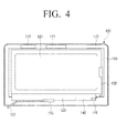
- FIG. 4 is a view illustrating a display unit having a converting circuit disposed in a display driving board of the display unit according to an exemplary embodiment of the present invention.
- the display unit 120 is connected to the main board 111 by hinges and may pivot with respect to the main body unit 110 by a predetermined angle.
- the display unit 120 may include any suitable apparatus that can display data, such as a liquid crystal display module, a field emission display module or any other similar display module.
- the display unit 120 may include a screen portion 121 in order to output various data and information of the mobile electronic apparatus 100 according to control of the main board 111 and a display driving board 123 (see FIG. 4 ) for driving the screen portion 121.
- the display driving board 123 drives the screen portion 121 according to control signals from the main board 111.
- a Time-CONtrol (T-CON) board may be used as the display driving board 123.
- the display unit 120 may further include sub-boards that can perform other functions in addition to the display driving board 123. As shown in FIG. 4 , the display unit 120 may include a camera module board 171, a communication board 172, an antenna board 173, and other similar boards or components that are disposed around the screen portion 121.
- the communication board 172 may include a variety of mobile and wireless communication system boards.
- the display unit 120 includes the converting circuit 140 that stabilizes the electricity generated by the solar cell module 130 and supplies it to the main body unit 110. That is, the converting circuit 140 is disposed inside a housing that forms the display unit 120.
- the converting circuit 140 converts unstable electric power output from the solar cell module 130 that has an unstable voltage that is altered or modified according to a change of sunlight so as to be stable electric power having a constant voltage.
- a solar cell DC/DC converter may be used as the converting circuit 140.
- the converting circuit 140 may be arranged in the display unit 120 according to various methods and designs of the mobile electronic apparatus 100.
- the converting circuit 140 may be formed integrally with the display driving board 123 of the display unit 120.
- the converting circuit 140 is formed on a portion of the display driving board 123 so that the display driving board 123 and the converting circuit 140 are formed as one single board. If the display driving board 123 and the converting circuit 140 are formed as a single board as described above, a space on the board may be reserved and the electric power output from the converting circuit 140 may be supplied to the main body unit 110 using a display cable 127 (see FIG. 4 ) connecting the display driving board 123 and the main board 111.
- the display cable 127 is connected to the display driving board 123 by a display connector 125.
- a connector 141 of the display driving board 123 connects the solar cell module 130 and the converting circuit 140.
- a solar cell cable 132 coupled to the solar cell module 130 is connected to the connector 141.
- the display cable 127 In a case when the display cable 127 is used to transmit electric power that has been converted in the converting circuit 140 to the main body unit 110, if the display cable 127 has extra wires that are not used for the electrical connection to the display unit 120 and the main board 111, then, the extra wires may be used to transmit the electric power output from the converting circuit 140. If the display cable 127 does not have the extra wires, the wires for transmitting the electric power output from the converting circuit 140 may be added as additional wires to the display cable 127.
- FIG. 5 is a view illustrating a display unit having a converting circuit formed on a separate exclusive board according to an exemplary embodiment of the present invention.
- the converting circuit 140 may be formed on an exclusive board 140' that is separated from the display driving board 123.
- the converting circuit 140 is formed on the separate converter board 140' and the converter board 140' is disposed inside the display unit 120. If the converting circuit 140 is formed on the separate converter board 140', then the converting circuit 140 may be arranged at an optimum position according to the design of the display unit 120. In this case, the electric power and signals are transmitted to the main board 111 using the display cable 127 connecting the display driving board 123 and the main board 111 and using a separate converter board cable 143 connecting the exclusive converter board 140' to the main board 111.
- the display connector 125 is used to connect the display cable 127 to the display driving board 123.
- a connector 142 of the exclusive converter board 140' is used to connect the solar cell module 130 to the converter board 140'.
- the solar cell cable 132 is coupled to the solar cell module 130 and is connected to the connector 142.
- FIG. 6 is a view illustrating a display unit having a converting circuit formed on a separate camera module board according to an exemplary embodiment of the present invention.
- the converting circuit 140 may be formed integrally with one sub-board 171 from among sub-boards 171, 172, and 173 that are disposed in the display unit 120 and have different functions than the display driving board 123.
- the converting circuit 140 is formed on a camera module board 171' such that the camera module board 171' may perform a converter function in addition to the camera function.
- the present invention is not limited to the exemplary embodiment disclosed above, and the sub-board on which the converting circuit 140 is disposed is not limited to the camera module board 171', as described above.
- the converting circuit 140 may be disposed on any one among sub-boards 171, 172, and 173 having specific functions and disposed inside the display unit 120, such as a communication board 172, which may be a 3rd Generation (3G) system board or a 4th Generation (4G) system board, the antenna board 173, the camera module board 171', or any other suitable sub-board.
- 3G 3rd Generation
- 4G 4th Generation
- the electric power and the signals are transmitted using the display cable 127 connecting the display driving board 123 and the main board 111 and using a separate converter cable 143' connecting any one of the sub-boards 171, 172, and 173.
- a connector 142' provided in the sub-boards 171, 172, and 173 is used to connect the solar cell module 130 and the converting circuit 140.
- the solar cell cable 132 is coupled to the solar cell module 130 and is also connected to the connector 142'.
- the display driving board 123 is connected with the main board 111 of the main body unit 110 via the display cable 127.
- the display cable 127 is connected to the display driving board 123 by the display connector 125. Ground parts of the display cable 127 are shielded in order to prevent noise, such as Electromagnetic Interference (EMI).
- EMI Electromagnetic Interference
- the electric power converted by the converting circuit 140 is transmitted to the main board 111 via the display cable 127.
- the main board 111 controls the electric power transmitted via the display cable 127 so as to charge the rechargeable battery or to be supplied to other elements of the mobile electronic apparatus 100 that require power.
- the electric power stabilized by the converting circuit 140 is transmitted to the main board 111 of the main body unit 110 through the shielded display cable 127, the possibility of loss of electric power may be reduced compared to related-art mobile electronic apparatuses so as to transmit unstable electric power generated in the solar cells to the main body unit 10 via a separate electric power supply cable.
- a length of a wire through which unstable electric power flows is shorter than that in the related-art mobile electronic apparatus, so as to reduce the possibility or the amount of electrical noise and interference.
- the converting circuit 40 is disposed on the main board 30 of the main body unit 10 and the solar cells are disposed in the display unit 20, a length of the wire connecting the converting circuit 40 and the solar cells is longer than that of a wire used in the mobile electronic apparatus 100 according to an exemplary embodiment of the present disclosure.
- the solar cell module 130 converts solar energy into electric power and is disposed on a rear surface of the display unit 120.
- the solar cell module 130 is disposed on the rear surface of the display unit 120, or in other words, on a surface of the display unit 120 that is opposite to a surface on which the screen portion 121 is disposed.
- the solar cell module 130 may be directly fixed to the rear surface of the display unit 120.
- the present invention is not limited thereto, and the solar cell module 130 may be attached or disposed on the rear surface of the display unit 120 in a variety of suitable manners.
- the electric power generated by the solar cell module 130 is transmitted to the converting circuit 140 through the solar cell cable 132.
- a fixing bracket 150 may be disposed between the solar cell module 130 and the display unit 120.
- the fixing bracket 150 allows the solar cell module 130 to be fixed to the display unit 120 and buffers the solar cell module 130.
- the fixing bracket 150 is formed as a substantially rectangular frame having an opening at a central portion 154 that corresponds to the circumference of the solar cell module 130.
- the fixing bracket 150 may be formed to secure the solar cell module 130 while fixing the display unit 120 to a case 129.
- the fixing bracket 150 has a plurality of fixing portions 151 which are projected from the circumference of the fixing bracket 150 so as to fix the fixing bracket 150 to the case 129.
- the fixing bracket 150 also includes a plurality of fixing holes 153 so as to attach the display unit 120 to the solar cell module 130.
- the fixing bracket 150 can be fixed to the case 129 by using fastening elements such as screws or any other suitable fastening elements.
- the solar cell module 130 and the display unit 120 can be fixed to the fixing bracket 150 by using the fastening elements.
- a cushioning member 155 may be disposed in the central portion 154 of the fixing bracket 150.
- the cushioning member 155 has two slim band shapes that are disposed in the central portion 154 of the fixing bracket 150.
- the shape of the cushioning member 155 is not limited thereto, and may be formed in any suitable shape.
- the cushioning member 155 may be formed to have the same size and shape as those of the inner space 154 of the fixing bracket 150. Therefore, the cushioning member 155 may be formed to be various sizes and shapes as long as the cushioning member 155 may be disposed inside the inner space 154.
- the cushioning member 155 may be formed of a material that can absorb shocks, such as a sponge or any other suitable material, in order to absorb external shocks applied to the solar cell module 130.
- the fixing bracket 150 may be formed of a material having good thermal conductivity. If the fixing bracket 150 is made of such a material, then the fixing bracket 150 can absorb heat generated by operation of the solar cell module 130 and may evenly diffuse the heat to the whole of the display unit 120. Thus, the temperature increase due to use of the solar cell module 130 may be reduced. Therefore, electric power generating efficiency of the solar cell module 130 may be increased. Also, the fixing bracket 150 may affix the solar cell cable 132 that is connected between the converting circuit 140 and the solar cell module 130.
- a protection cover 160 may be disposed above the solar cell module 130 in order to prevent the solar cell module 130 from being damaged and contaminated.
- One example of the protection cover 160 is illustrated in FIG. 3 .
- the protection cover 160 is made of a transparent material through which sunlight can pass. If the protection cover 160 is disposed above the solar cell module 130, as described above, then the solar cell module 130 may be prevented from being damaged by the external shocks or by contamination.
- FIG. 7 is a plan view illustrating a gap maintaining member disposed between a protection cover and a solar cell module in a mobile electronic apparatus according to an exemplary embodiment of the present invention
- FIG. 8 is a view illustrating an example of wave patterns generated when pressure is applied to a protection cover of a mobile electronic apparatus according to an exemplary embodiment of the present invention.
- the protection cover 160 when the protection cover 160 is disposed above the solar cell module 130 there is a gap between the protection cover 160 and the solar cell module 130. If the solar cell module 130 has a size of 8 inches or more, then a shape of the protection cover 160 may be altered so as to droop down due to the weight of the protection cover 160. If the shape of the protection cover 160 is altered, the gap between the solar cell module 130 and the protection cover 160 is not constant so that the protection cover 160 may be variously in contact with the solar cell module 130. In addition, when external pressure is applied to the protection cover 160 in such a case, as illustrated in FIG. 8 , wave patterns 170 may be formed on the top surface of the solar cell module 130. Therefore, as shown in FIG.
- a gap remaining member 161 may be disposed in the space between the protection cover 160 and the solar cell module 130 in order to prevent the protection cover 160 from being in contact with the solar cell module 130 and to prevent the wave patterns from occurring due to a drooping of the protection cover 160.
- the gap maintaining member 161 is attached to the solar cell module 130 so as to occupy the gap between the solar cell module 130 and the protection cover 160.
- the gap maintaining member 161 may be disposed on portions of the solar cell module 130 where the solar cells 131 do not exist on a top surface of the solar cell module 130.
- FIG. 7 illustrates two gap maintaining members 161 which are disposed in parallel to each other on portions of the solar cell module 130 which do not generate electric power.
- the present invention is not limited to the present exemplary embodiment of the gap maintaining member 161, and other suitable shapes and arranging positions of the gap maintaining member 161 may be used.
- the gap maintaining member 161 may be formed as various shapes as long as the gap maintaining member 161 uniformly maintains the gap between the protection cover 160 and the solar cell module 130 and does not interfere with electric power production of the solar cell module 130.
- an insulating tape may be used as the gap maintaining member 161.
- the solar cell module and the converting circuit are located close to each other. Therefore, the length of the wire through which unstable electricity flows between the solar cell module and the converting circuit is shorter than that of the related-art mobile electronic apparatus. As a result, a decline of power generation efficiency of the solar cell module that may be generated by unstable electric power may be minimized.
- the electrical noise and interference may be minimized so that the noise generated by the solar cell module affects other elements.
- the fixing bracket is disposed between the display unit and the solar cell module so as to affix the solar cell module and to effectively diffuse heat generated in the solar cell module, the electric power generation efficiency of the solar cell module may be increased.
- the protection cover may be prevented from being in contact with the solar cell module.
Landscapes
- Engineering & Computer Science (AREA)
- Theoretical Computer Science (AREA)
- Physics & Mathematics (AREA)
- General Engineering & Computer Science (AREA)
- General Physics & Mathematics (AREA)
- Computer Hardware Design (AREA)
- Power Engineering (AREA)
- Human Computer Interaction (AREA)
- Mathematical Physics (AREA)
- Signal Processing (AREA)
- Devices For Indicating Variable Information By Combining Individual Elements (AREA)
- Power Sources (AREA)
- Telephone Set Structure (AREA)
- Photovoltaic Devices (AREA)
Applications Claiming Priority (1)
| Application Number | Priority Date | Filing Date | Title |
|---|---|---|---|
| KR1020110088212A KR101414469B1 (ko) | 2011-08-31 | 2011-08-31 | 태양전지를 구비한 휴대용 전자기기 |
Publications (3)
| Publication Number | Publication Date |
|---|---|
| EP2565746A2 true EP2565746A2 (fr) | 2013-03-06 |
| EP2565746A3 EP2565746A3 (fr) | 2016-01-06 |
| EP2565746B1 EP2565746B1 (fr) | 2019-03-06 |
Family
ID=46085344
Family Applications (1)
| Application Number | Title | Priority Date | Filing Date |
|---|---|---|---|
| EP12162679.0A Not-in-force EP2565746B1 (fr) | 2011-08-31 | 2012-03-30 | Appareil électronique mobile comportant des cellules solaires |
Country Status (4)
| Country | Link |
|---|---|
| US (1) | US9354682B2 (fr) |
| EP (1) | EP2565746B1 (fr) |
| KR (1) | KR101414469B1 (fr) |
| CN (1) | CN102968167B (fr) |
Families Citing this family (7)
| Publication number | Priority date | Publication date | Assignee | Title |
|---|---|---|---|---|
| US9398422B2 (en) | 2014-11-05 | 2016-07-19 | Beco, Inc. | Systems, methods and apparatus for light enabled indoor positioning and reporting |
| KR102562895B1 (ko) * | 2015-12-15 | 2023-08-04 | 삼성디스플레이 주식회사 | 표시 장치의 제조장치 및 표시 장치의 제조방법 |
| US10231346B2 (en) * | 2016-05-27 | 2019-03-12 | Lg Electronics Inc. | Display device |
| CN109615941B (zh) * | 2019-01-21 | 2020-09-15 | 合肥状元郎电子科技有限公司 | 一种太阳能电子书包 |
| WO2021188675A1 (fr) * | 2020-03-20 | 2021-09-23 | Garmin Switzerland Gmbh | Cellules photovoltaïques à visibilité d'isolation améliorée |
| CN115461879A (zh) * | 2020-03-20 | 2022-12-09 | 佳明瑞士有限责任公司 | 用于便携式电子设备的多单元光伏电池 |
| US11670724B2 (en) | 2020-03-20 | 2023-06-06 | Garmin Switzerland Gmbh | Photovoltaic cells for a portable electronic device |
Family Cites Families (19)
| Publication number | Priority date | Publication date | Assignee | Title |
|---|---|---|---|---|
| JPH0283640U (fr) * | 1988-12-09 | 1990-06-28 | ||
| CN2100660U (zh) * | 1991-08-31 | 1992-04-01 | 马希光 | 可充电太阳能计算机 |
| JP2001178017A (ja) * | 1999-12-15 | 2001-06-29 | Nec Corp | バッテリパック及びその充電回路 |
| KR200191762Y1 (ko) * | 2000-03-03 | 2000-08-16 | 임성묵 | 솔라셀이 부착된 노트북컴퓨터 |
| US20020088486A1 (en) * | 2001-01-11 | 2002-07-11 | I-Ming Chen | Solar-powered device for charging a battery unit of a mobile telephone handset |
| KR100434048B1 (ko) * | 2001-10-05 | 2004-06-04 | 엘지전자 주식회사 | 휴대형 전자기기의 엘시디 모듈 연결장치 |
| KR20030068763A (ko) * | 2002-02-18 | 2003-08-25 | 박창복 | 노트북컴퓨터에서 솔라를 이용한 전원충전장치 |
| KR20040013640A (ko) * | 2002-08-07 | 2004-02-14 | 삼성전자주식회사 | 태양열전지를 이용하여 전원을 충전할 수 있는 휴대용 기기 |
| CN1332286C (zh) | 2003-11-24 | 2007-08-15 | 佛山市顺德区顺达电脑厂有限公司 | 具有辅助电力供应之可携式电脑电源管理装置及方法 |
| US20060170223A1 (en) * | 2005-02-01 | 2006-08-03 | Homer Steven S | Computer latch |
| CN101145743A (zh) | 2006-09-11 | 2008-03-19 | 官有占 | 太阳电池高效发电散热系统 |
| US20080094025A1 (en) * | 2006-10-20 | 2008-04-24 | Rosenblatt Michael N | Solar cells on portable devices |
| CN101169677A (zh) | 2006-10-24 | 2008-04-30 | 鸿富锦精密工业(深圳)有限公司 | 笔记本电脑 |
| US7952866B2 (en) * | 2009-04-21 | 2011-05-31 | Seung Min Lee | Portable computer |
| JP5491063B2 (ja) * | 2009-04-27 | 2014-05-14 | キヤノン株式会社 | 表示装置及び調整機構 |
| JP2011008086A (ja) * | 2009-06-26 | 2011-01-13 | Toshiba Corp | 電子機器 |
| TWI467781B (zh) * | 2010-10-29 | 2015-01-01 | Au Optronics Corp | 電子裝置 |
| US20120110354A1 (en) * | 2010-11-02 | 2012-05-03 | Sunrex Technology Corp. | Holder with solar module for holding portable electronic devices |
| KR20120053149A (ko) * | 2010-11-17 | 2012-05-25 | 삼성전자주식회사 | 태양 전지를 이용한 전원 공급 방법, 이를 수행하기 위한 전원 공급 장치 및 이 전원 공급 장치를 포함하는 표시 장치 |
-
2011
- 2011-08-31 KR KR1020110088212A patent/KR101414469B1/ko not_active Expired - Fee Related
-
2012
- 2012-03-30 EP EP12162679.0A patent/EP2565746B1/fr not_active Not-in-force
- 2012-08-24 US US13/594,081 patent/US9354682B2/en active Active
- 2012-08-27 CN CN201210308778.XA patent/CN102968167B/zh not_active Expired - Fee Related
Non-Patent Citations (1)
| Title |
|---|
| None |
Also Published As
| Publication number | Publication date |
|---|---|
| US20130050948A1 (en) | 2013-02-28 |
| CN102968167B (zh) | 2016-12-28 |
| US9354682B2 (en) | 2016-05-31 |
| CN102968167A (zh) | 2013-03-13 |
| EP2565746B1 (fr) | 2019-03-06 |
| KR101414469B1 (ko) | 2014-07-03 |
| KR20130024647A (ko) | 2013-03-08 |
| EP2565746A3 (fr) | 2016-01-06 |
Similar Documents
| Publication | Publication Date | Title |
|---|---|---|
| EP2565746B1 (fr) | Appareil électronique mobile comportant des cellules solaires | |
| KR102184621B1 (ko) | 방열 쉬트를 구비한 이동 통신 단말기 | |
| US9268376B2 (en) | Mobile computing device dock station with headset jack heat pipe interface | |
| US10333195B2 (en) | Electronic device | |
| CN105376465B (zh) | 一种便携式无线摄像机 | |
| US20090295234A1 (en) | Portable solar power supply system and its applying device | |
| KR101691797B1 (ko) | 이동 단말기 | |
| US20150185408A1 (en) | Protective cover | |
| JP4635918B2 (ja) | 携帯電話機の保護カバーおよび携帯電話機の充電システム。 | |
| CN101452970B (zh) | 太阳能电池模组及便携式电子装置 | |
| CN108600446A (zh) | 移动终端 | |
| CN208014281U (zh) | 显示屏箱体、显示装置和拼接式显示器件 | |
| KR20140130806A (ko) | 태양전지를 이용한 휴대용 충전장치 | |
| US20120214556A1 (en) | Method and Apparatus for Solar Cell Light Concentrator Panel | |
| CN213904765U (zh) | 一种显示装置 | |
| CN109004756A (zh) | 无线充电系统 | |
| CN115811718A (zh) | 一种控制器 | |
| CN202940752U (zh) | 一种离网逆变一体机 | |
| CN217789664U (zh) | Wifi模组及电子设备 | |
| CN222260020U (zh) | 能引出信号及取电的皮套键盘 | |
| CN204832683U (zh) | 一种头戴显示装置 | |
| JP2009032806A (ja) | 電子機器用電力供給ケース | |
| US9372506B2 (en) | Electronic device | |
| CN219181219U (zh) | 一种便携式移动电源 | |
| CN213071728U (zh) | 一种便携式备用电源 |
Legal Events
| Date | Code | Title | Description |
|---|---|---|---|
| PUAI | Public reference made under article 153(3) epc to a published international application that has entered the european phase |
Free format text: ORIGINAL CODE: 0009012 |
|
| 17P | Request for examination filed |
Effective date: 20120330 |
|
| AK | Designated contracting states |
Kind code of ref document: A2 Designated state(s): AL AT BE BG CH CY CZ DE DK EE ES FI FR GB GR HR HU IE IS IT LI LT LU LV MC MK MT NL NO PL PT RO RS SE SI SK SM TR |
|
| AX | Request for extension of the european patent |
Extension state: BA ME |
|
| PUAL | Search report despatched |
Free format text: ORIGINAL CODE: 0009013 |
|
| AK | Designated contracting states |
Kind code of ref document: A3 Designated state(s): AL AT BE BG CH CY CZ DE DK EE ES FI FR GB GR HR HU IE IS IT LI LT LU LV MC MK MT NL NO PL PT RO RS SE SI SK SM TR |
|
| AX | Request for extension of the european patent |
Extension state: BA ME |
|
| RIC1 | Information provided on ipc code assigned before grant |
Ipc: G06F 1/26 20060101AFI20151130BHEP Ipc: H04M 1/21 20060101ALN20151130BHEP Ipc: G06F 1/16 20060101ALI20151130BHEP Ipc: H02J 7/35 20060101ALI20151130BHEP |
|
| STAA | Information on the status of an ep patent application or granted ep patent |
Free format text: STATUS: EXAMINATION IS IN PROGRESS |
|
| 17Q | First examination report despatched |
Effective date: 20170629 |
|
| GRAP | Despatch of communication of intention to grant a patent |
Free format text: ORIGINAL CODE: EPIDOSNIGR1 |
|
| STAA | Information on the status of an ep patent application or granted ep patent |
Free format text: STATUS: GRANT OF PATENT IS INTENDED |
|
| RIC1 | Information provided on ipc code assigned before grant |
Ipc: H04M 1/21 20060101ALN20180910BHEP Ipc: G06F 1/16 20060101ALI20180910BHEP Ipc: G06F 1/26 20060101AFI20180910BHEP Ipc: H02J 7/35 20060101ALI20180910BHEP |
|
| INTG | Intention to grant announced |
Effective date: 20180928 |
|
| GRAS | Grant fee paid |
Free format text: ORIGINAL CODE: EPIDOSNIGR3 |
|
| GRAA | (expected) grant |
Free format text: ORIGINAL CODE: 0009210 |
|
| STAA | Information on the status of an ep patent application or granted ep patent |
Free format text: STATUS: THE PATENT HAS BEEN GRANTED |
|
| AK | Designated contracting states |
Kind code of ref document: B1 Designated state(s): AL AT BE BG CH CY CZ DE DK EE ES FI FR GB GR HR HU IE IS IT LI LT LU LV MC MK MT NL NO PL PT RO RS SE SI SK SM TR |
|
| REG | Reference to a national code |
Ref country code: GB Ref legal event code: FG4D |
|
| REG | Reference to a national code |
Ref country code: CH Ref legal event code: EP Ref country code: AT Ref legal event code: REF Ref document number: 1105402 Country of ref document: AT Kind code of ref document: T Effective date: 20190315 |
|
| REG | Reference to a national code |
Ref country code: DE Ref legal event code: R096 Ref document number: 602012057359 Country of ref document: DE |
|
| REG | Reference to a national code |
Ref country code: IE Ref legal event code: FG4D |
|
| REG | Reference to a national code |
Ref country code: NL Ref legal event code: FP |
|
| REG | Reference to a national code |
Ref country code: LT Ref legal event code: MG4D |
|
| PG25 | Lapsed in a contracting state [announced via postgrant information from national office to epo] |
Ref country code: SE Free format text: LAPSE BECAUSE OF FAILURE TO SUBMIT A TRANSLATION OF THE DESCRIPTION OR TO PAY THE FEE WITHIN THE PRESCRIBED TIME-LIMIT Effective date: 20190306 Ref country code: NO Free format text: LAPSE BECAUSE OF FAILURE TO SUBMIT A TRANSLATION OF THE DESCRIPTION OR TO PAY THE FEE WITHIN THE PRESCRIBED TIME-LIMIT Effective date: 20190606 Ref country code: FI Free format text: LAPSE BECAUSE OF FAILURE TO SUBMIT A TRANSLATION OF THE DESCRIPTION OR TO PAY THE FEE WITHIN THE PRESCRIBED TIME-LIMIT Effective date: 20190306 Ref country code: LT Free format text: LAPSE BECAUSE OF FAILURE TO SUBMIT A TRANSLATION OF THE DESCRIPTION OR TO PAY THE FEE WITHIN THE PRESCRIBED TIME-LIMIT Effective date: 20190306 |
|
| PG25 | Lapsed in a contracting state [announced via postgrant information from national office to epo] |
Ref country code: GR Free format text: LAPSE BECAUSE OF FAILURE TO SUBMIT A TRANSLATION OF THE DESCRIPTION OR TO PAY THE FEE WITHIN THE PRESCRIBED TIME-LIMIT Effective date: 20190607 Ref country code: BG Free format text: LAPSE BECAUSE OF FAILURE TO SUBMIT A TRANSLATION OF THE DESCRIPTION OR TO PAY THE FEE WITHIN THE PRESCRIBED TIME-LIMIT Effective date: 20190606 Ref country code: RS Free format text: LAPSE BECAUSE OF FAILURE TO SUBMIT A TRANSLATION OF THE DESCRIPTION OR TO PAY THE FEE WITHIN THE PRESCRIBED TIME-LIMIT Effective date: 20190306 Ref country code: HR Free format text: LAPSE BECAUSE OF FAILURE TO SUBMIT A TRANSLATION OF THE DESCRIPTION OR TO PAY THE FEE WITHIN THE PRESCRIBED TIME-LIMIT Effective date: 20190306 Ref country code: LV Free format text: LAPSE BECAUSE OF FAILURE TO SUBMIT A TRANSLATION OF THE DESCRIPTION OR TO PAY THE FEE WITHIN THE PRESCRIBED TIME-LIMIT Effective date: 20190306 |
|
| REG | Reference to a national code |
Ref country code: AT Ref legal event code: MK05 Ref document number: 1105402 Country of ref document: AT Kind code of ref document: T Effective date: 20190306 |
|
| PG25 | Lapsed in a contracting state [announced via postgrant information from national office to epo] |
Ref country code: CZ Free format text: LAPSE BECAUSE OF FAILURE TO SUBMIT A TRANSLATION OF THE DESCRIPTION OR TO PAY THE FEE WITHIN THE PRESCRIBED TIME-LIMIT Effective date: 20190306 Ref country code: RO Free format text: LAPSE BECAUSE OF FAILURE TO SUBMIT A TRANSLATION OF THE DESCRIPTION OR TO PAY THE FEE WITHIN THE PRESCRIBED TIME-LIMIT Effective date: 20190306 Ref country code: SK Free format text: LAPSE BECAUSE OF FAILURE TO SUBMIT A TRANSLATION OF THE DESCRIPTION OR TO PAY THE FEE WITHIN THE PRESCRIBED TIME-LIMIT Effective date: 20190306 Ref country code: EE Free format text: LAPSE BECAUSE OF FAILURE TO SUBMIT A TRANSLATION OF THE DESCRIPTION OR TO PAY THE FEE WITHIN THE PRESCRIBED TIME-LIMIT Effective date: 20190306 Ref country code: IT Free format text: LAPSE BECAUSE OF FAILURE TO SUBMIT A TRANSLATION OF THE DESCRIPTION OR TO PAY THE FEE WITHIN THE PRESCRIBED TIME-LIMIT Effective date: 20190306 Ref country code: ES Free format text: LAPSE BECAUSE OF FAILURE TO SUBMIT A TRANSLATION OF THE DESCRIPTION OR TO PAY THE FEE WITHIN THE PRESCRIBED TIME-LIMIT Effective date: 20190306 Ref country code: AL Free format text: LAPSE BECAUSE OF FAILURE TO SUBMIT A TRANSLATION OF THE DESCRIPTION OR TO PAY THE FEE WITHIN THE PRESCRIBED TIME-LIMIT Effective date: 20190306 Ref country code: PT Free format text: LAPSE BECAUSE OF FAILURE TO SUBMIT A TRANSLATION OF THE DESCRIPTION OR TO PAY THE FEE WITHIN THE PRESCRIBED TIME-LIMIT Effective date: 20190706 |
|
| REG | Reference to a national code |
Ref country code: CH Ref legal event code: PL |
|
| PG25 | Lapsed in a contracting state [announced via postgrant information from national office to epo] |
Ref country code: LU Free format text: LAPSE BECAUSE OF NON-PAYMENT OF DUE FEES Effective date: 20190330 Ref country code: SM Free format text: LAPSE BECAUSE OF FAILURE TO SUBMIT A TRANSLATION OF THE DESCRIPTION OR TO PAY THE FEE WITHIN THE PRESCRIBED TIME-LIMIT Effective date: 20190306 Ref country code: PL Free format text: LAPSE BECAUSE OF FAILURE TO SUBMIT A TRANSLATION OF THE DESCRIPTION OR TO PAY THE FEE WITHIN THE PRESCRIBED TIME-LIMIT Effective date: 20190306 |
|
| REG | Reference to a national code |
Ref country code: BE Ref legal event code: MM Effective date: 20190331 |
|
| REG | Reference to a national code |
Ref country code: DE Ref legal event code: R097 Ref document number: 602012057359 Country of ref document: DE |
|
| PG25 | Lapsed in a contracting state [announced via postgrant information from national office to epo] |
Ref country code: AT Free format text: LAPSE BECAUSE OF FAILURE TO SUBMIT A TRANSLATION OF THE DESCRIPTION OR TO PAY THE FEE WITHIN THE PRESCRIBED TIME-LIMIT Effective date: 20190306 Ref country code: IS Free format text: LAPSE BECAUSE OF FAILURE TO SUBMIT A TRANSLATION OF THE DESCRIPTION OR TO PAY THE FEE WITHIN THE PRESCRIBED TIME-LIMIT Effective date: 20190706 |
|
| PLBE | No opposition filed within time limit |
Free format text: ORIGINAL CODE: 0009261 |
|
| STAA | Information on the status of an ep patent application or granted ep patent |
Free format text: STATUS: NO OPPOSITION FILED WITHIN TIME LIMIT |
|
| PG25 | Lapsed in a contracting state [announced via postgrant information from national office to epo] |
Ref country code: LI Free format text: LAPSE BECAUSE OF NON-PAYMENT OF DUE FEES Effective date: 20190331 Ref country code: CH Free format text: LAPSE BECAUSE OF NON-PAYMENT OF DUE FEES Effective date: 20190331 Ref country code: IE Free format text: LAPSE BECAUSE OF NON-PAYMENT OF DUE FEES Effective date: 20190330 Ref country code: DK Free format text: LAPSE BECAUSE OF FAILURE TO SUBMIT A TRANSLATION OF THE DESCRIPTION OR TO PAY THE FEE WITHIN THE PRESCRIBED TIME-LIMIT Effective date: 20190306 Ref country code: MC Free format text: LAPSE BECAUSE OF FAILURE TO SUBMIT A TRANSLATION OF THE DESCRIPTION OR TO PAY THE FEE WITHIN THE PRESCRIBED TIME-LIMIT Effective date: 20190306 |
|
| 26N | No opposition filed |
Effective date: 20191209 |
|
| PG25 | Lapsed in a contracting state [announced via postgrant information from national office to epo] |
Ref country code: BE Free format text: LAPSE BECAUSE OF NON-PAYMENT OF DUE FEES Effective date: 20190331 Ref country code: SI Free format text: LAPSE BECAUSE OF FAILURE TO SUBMIT A TRANSLATION OF THE DESCRIPTION OR TO PAY THE FEE WITHIN THE PRESCRIBED TIME-LIMIT Effective date: 20190306 |
|
| PG25 | Lapsed in a contracting state [announced via postgrant information from national office to epo] |
Ref country code: TR Free format text: LAPSE BECAUSE OF FAILURE TO SUBMIT A TRANSLATION OF THE DESCRIPTION OR TO PAY THE FEE WITHIN THE PRESCRIBED TIME-LIMIT Effective date: 20190306 |
|
| PG25 | Lapsed in a contracting state [announced via postgrant information from national office to epo] |
Ref country code: FR Free format text: LAPSE BECAUSE OF NON-PAYMENT OF DUE FEES Effective date: 20190506 Ref country code: MT Free format text: LAPSE BECAUSE OF NON-PAYMENT OF DUE FEES Effective date: 20190330 |
|
| PGFP | Annual fee paid to national office [announced via postgrant information from national office to epo] |
Ref country code: NL Payment date: 20210209 Year of fee payment: 10 |
|
| PG25 | Lapsed in a contracting state [announced via postgrant information from national office to epo] |
Ref country code: CY Free format text: LAPSE BECAUSE OF FAILURE TO SUBMIT A TRANSLATION OF THE DESCRIPTION OR TO PAY THE FEE WITHIN THE PRESCRIBED TIME-LIMIT Effective date: 20190306 |
|
| PGFP | Annual fee paid to national office [announced via postgrant information from national office to epo] |
Ref country code: GB Payment date: 20210216 Year of fee payment: 10 |
|
| PG25 | Lapsed in a contracting state [announced via postgrant information from national office to epo] |
Ref country code: HU Free format text: LAPSE BECAUSE OF FAILURE TO SUBMIT A TRANSLATION OF THE DESCRIPTION OR TO PAY THE FEE WITHIN THE PRESCRIBED TIME-LIMIT; INVALID AB INITIO Effective date: 20120330 |
|
| PG25 | Lapsed in a contracting state [announced via postgrant information from national office to epo] |
Ref country code: MK Free format text: LAPSE BECAUSE OF FAILURE TO SUBMIT A TRANSLATION OF THE DESCRIPTION OR TO PAY THE FEE WITHIN THE PRESCRIBED TIME-LIMIT Effective date: 20190306 |
|
| REG | Reference to a national code |
Ref country code: NL Ref legal event code: MM Effective date: 20220401 |
|
| GBPC | Gb: european patent ceased through non-payment of renewal fee |
Effective date: 20220330 |
|
| PG25 | Lapsed in a contracting state [announced via postgrant information from national office to epo] |
Ref country code: NL Free format text: LAPSE BECAUSE OF NON-PAYMENT OF DUE FEES Effective date: 20220401 Ref country code: GB Free format text: LAPSE BECAUSE OF NON-PAYMENT OF DUE FEES Effective date: 20220330 |
|
| PGFP | Annual fee paid to national office [announced via postgrant information from national office to epo] |
Ref country code: DE Payment date: 20240220 Year of fee payment: 13 |
|
| REG | Reference to a national code |
Ref country code: DE Ref legal event code: R119 Ref document number: 602012057359 Country of ref document: DE |
|
| PG25 | Lapsed in a contracting state [announced via postgrant information from national office to epo] |
Ref country code: DE Free format text: LAPSE BECAUSE OF NON-PAYMENT OF DUE FEES Effective date: 20251001 |