EP2565925A2 - Festkörperabbildungsvorrichtung - Google Patents
Festkörperabbildungsvorrichtung Download PDFInfo
- Publication number
- EP2565925A2 EP2565925A2 EP12004985A EP12004985A EP2565925A2 EP 2565925 A2 EP2565925 A2 EP 2565925A2 EP 12004985 A EP12004985 A EP 12004985A EP 12004985 A EP12004985 A EP 12004985A EP 2565925 A2 EP2565925 A2 EP 2565925A2
- Authority
- EP
- European Patent Office
- Prior art keywords
- region
- pixel
- photodiode
- semiconductor
- semiconductor region
- Prior art date
- Legal status (The legal status is an assumption and is not a legal conclusion. Google has not performed a legal analysis and makes no representation as to the accuracy of the status listed.)
- Withdrawn
Links
- 238000003384 imaging method Methods 0.000 title claims description 32
- 239000004065 semiconductor Substances 0.000 claims description 79
- 238000002955 isolation Methods 0.000 claims description 11
- 206010034972 Photosensitivity reaction Diseases 0.000 abstract description 13
- 230000003247 decreasing effect Effects 0.000 abstract description 13
- 230000036211 photosensitivity Effects 0.000 abstract description 13
- 230000002093 peripheral effect Effects 0.000 abstract description 12
- 230000005684 electric field Effects 0.000 abstract description 9
- 230000035945 sensitivity Effects 0.000 abstract description 7
- 239000010410 layer Substances 0.000 description 53
- 239000012535 impurity Substances 0.000 description 39
- 239000000758 substrate Substances 0.000 description 14
- 238000006243 chemical reaction Methods 0.000 description 8
- 230000000694 effects Effects 0.000 description 5
- 238000010586 diagram Methods 0.000 description 4
- 238000000034 method Methods 0.000 description 4
- 238000003491 array Methods 0.000 description 3
- 238000009792 diffusion process Methods 0.000 description 3
- 239000011241 protective layer Substances 0.000 description 3
- 230000000052 comparative effect Effects 0.000 description 2
- 230000005685 electric field effect Effects 0.000 description 2
- 230000003287 optical effect Effects 0.000 description 2
- 238000005549 size reduction Methods 0.000 description 2
- 241000080590 Niso Species 0.000 description 1
- 239000004020 conductor Substances 0.000 description 1
- 230000006866 deterioration Effects 0.000 description 1
- 238000009826 distribution Methods 0.000 description 1
- 238000009413 insulation Methods 0.000 description 1
- 239000012212 insulator Substances 0.000 description 1
- 239000011229 interlayer Substances 0.000 description 1
- 238000005468 ion implantation Methods 0.000 description 1
- 238000004519 manufacturing process Methods 0.000 description 1
Images






Classifications
-
- H—ELECTRICITY
- H10—SEMICONDUCTOR DEVICES; ELECTRIC SOLID-STATE DEVICES NOT OTHERWISE PROVIDED FOR
- H10F—INORGANIC SEMICONDUCTOR DEVICES SENSITIVE TO INFRARED RADIATION, LIGHT, ELECTROMAGNETIC RADIATION OF SHORTER WAVELENGTH OR CORPUSCULAR RADIATION
- H10F39/00—Integrated devices, or assemblies of multiple devices, comprising at least one element covered by group H10F30/00, e.g. radiation detectors comprising photodiode arrays
- H10F39/10—Integrated devices
- H10F39/12—Image sensors
- H10F39/15—Charge-coupled device [CCD] image sensors
-
- H—ELECTRICITY
- H10—SEMICONDUCTOR DEVICES; ELECTRIC SOLID-STATE DEVICES NOT OTHERWISE PROVIDED FOR
- H10F—INORGANIC SEMICONDUCTOR DEVICES SENSITIVE TO INFRARED RADIATION, LIGHT, ELECTROMAGNETIC RADIATION OF SHORTER WAVELENGTH OR CORPUSCULAR RADIATION
- H10F39/00—Integrated devices, or assemblies of multiple devices, comprising at least one element covered by group H10F30/00, e.g. radiation detectors comprising photodiode arrays
- H10F39/011—Manufacture or treatment of image sensors covered by group H10F39/12
- H10F39/014—Manufacture or treatment of image sensors covered by group H10F39/12 of CMOS image sensors
-
- H—ELECTRICITY
- H10—SEMICONDUCTOR DEVICES; ELECTRIC SOLID-STATE DEVICES NOT OTHERWISE PROVIDED FOR
- H10F—INORGANIC SEMICONDUCTOR DEVICES SENSITIVE TO INFRARED RADIATION, LIGHT, ELECTROMAGNETIC RADIATION OF SHORTER WAVELENGTH OR CORPUSCULAR RADIATION
- H10F39/00—Integrated devices, or assemblies of multiple devices, comprising at least one element covered by group H10F30/00, e.g. radiation detectors comprising photodiode arrays
- H10F39/10—Integrated devices
- H10F39/12—Image sensors
-
- H—ELECTRICITY
- H10—SEMICONDUCTOR DEVICES; ELECTRIC SOLID-STATE DEVICES NOT OTHERWISE PROVIDED FOR
- H10F—INORGANIC SEMICONDUCTOR DEVICES SENSITIVE TO INFRARED RADIATION, LIGHT, ELECTROMAGNETIC RADIATION OF SHORTER WAVELENGTH OR CORPUSCULAR RADIATION
- H10F39/00—Integrated devices, or assemblies of multiple devices, comprising at least one element covered by group H10F30/00, e.g. radiation detectors comprising photodiode arrays
- H10F39/10—Integrated devices
- H10F39/12—Image sensors
- H10F39/18—Complementary metal-oxide-semiconductor [CMOS] image sensors; Photodiode array image sensors
- H10F39/182—Colour image sensors
-
- H—ELECTRICITY
- H10—SEMICONDUCTOR DEVICES; ELECTRIC SOLID-STATE DEVICES NOT OTHERWISE PROVIDED FOR
- H10F—INORGANIC SEMICONDUCTOR DEVICES SENSITIVE TO INFRARED RADIATION, LIGHT, ELECTROMAGNETIC RADIATION OF SHORTER WAVELENGTH OR CORPUSCULAR RADIATION
- H10F39/00—Integrated devices, or assemblies of multiple devices, comprising at least one element covered by group H10F30/00, e.g. radiation detectors comprising photodiode arrays
- H10F39/80—Constructional details of image sensors
- H10F39/802—Geometry or disposition of elements in pixels, e.g. address-lines or gate electrodes
- H10F39/8027—Geometry of the photosensitive area
-
- H—ELECTRICITY
- H10—SEMICONDUCTOR DEVICES; ELECTRIC SOLID-STATE DEVICES NOT OTHERWISE PROVIDED FOR
- H10F—INORGANIC SEMICONDUCTOR DEVICES SENSITIVE TO INFRARED RADIATION, LIGHT, ELECTROMAGNETIC RADIATION OF SHORTER WAVELENGTH OR CORPUSCULAR RADIATION
- H10F39/00—Integrated devices, or assemblies of multiple devices, comprising at least one element covered by group H10F30/00, e.g. radiation detectors comprising photodiode arrays
- H10F39/80—Constructional details of image sensors
- H10F39/803—Pixels having integrated switching, control, storage or amplification elements
- H10F39/8033—Photosensitive area
-
- H—ELECTRICITY
- H10—SEMICONDUCTOR DEVICES; ELECTRIC SOLID-STATE DEVICES NOT OTHERWISE PROVIDED FOR
- H10F—INORGANIC SEMICONDUCTOR DEVICES SENSITIVE TO INFRARED RADIATION, LIGHT, ELECTROMAGNETIC RADIATION OF SHORTER WAVELENGTH OR CORPUSCULAR RADIATION
- H10F39/00—Integrated devices, or assemblies of multiple devices, comprising at least one element covered by group H10F30/00, e.g. radiation detectors comprising photodiode arrays
- H10F39/80—Constructional details of image sensors
- H10F39/807—Pixel isolation structures
Definitions
- the present invention concerns a solid-state imaging apparatus such as a CMOS sensor or a CCD sensor for obtaining image information and positional information by using a photoelectric conversion effect and it particularly relates to a solid-state imaging apparatus intending to reduce optical crosstalk by improvement in a well structure.
- Solid-state imaging apparatus represented by CMOS sensors and CCD sensors have been applied generally to video cameras, digital still cameras, etc.
- CMOS transistor is used as a switching device for selecting photoelectric conversion devices PD or a switching device for reading signal charges.
- an MOS transistor or CMOS transistor is used for peripheral circuits such as a control circuit and a signal processing circuit, and the apparatus have an advantage capable of manufacturing photoelectric conversion device PD, and the switching device, the peripheral circuits, etc. on one identical chip in a series of procedures.
- a plurality of pixels each provided with a photoelectric conversion device (photodiode PD) are arranged on a semiconductor substrate.
- Light incident on each of the pixels is photoelectrically converted by the photodiode to form and collect electric charges, the charges are transferred to a floating diffusion (FD) part, the potential fluctuation in the FD part is detected by an MOS transistor and converted into electric signals, which are amplified and outputted as video signals.
- FD floating diffusion
- the photoelectric conversion device PD is formed of a PN junction and, generally electric charges are collected by utilizing an electric field in a depletion layer generated by application of a voltage.
- a solid-state imaging apparatus for an incident light in a visible light region (380 nm to 830 nm)
- most of incident light is absorbed in a depth of about 5 ⁇ m from the Si surface to generate photocharges in the charge collection system.
- Japanese Unexamined Patent Application Publication No. 2004-031878 discloses an example of such technique.
- photoelectrically converted photocharges for the depth up to 5 ⁇ m region have to be introduced efficiently into a photoelectronic conversion device PD and read out.
- Deepening of PN junction as in Japanese Unexamined Patent Application Publication No. 2004-031878 is disadvantageous in the size-reduction of MOS transistor for switching on and off the charge transfer in a photoelectronic conversion device PD. Further, enlargement in the size of the MOS transistor size by deepening the PN junction involves a problem of decreasing the aperture ratio of the photoelectronic conversion device PD and lowering the photosensitivity. Further, increase in the voltage results in a problem of increasing the consumption power.
- Japanese Unexamined Patent Application Publication No. 2006-024907 discloses an example of a configuration of collecting electric charges by utilizing an internal electric field due to difference of impurity concentration between a photodiode PD and the substrate of an opposite conduction type without deepening the PN junction, thereby improving the sensitivity and decreasing the power consumption.
- electric charges are collected by utilizing the internal electric field due to the difference of the impurity concentration, no sufficient concentration gradient can be ensured for photoelectrons generated in a region deeper than the photodiode PD, the photoelectrons diffuse laterally in a region of weak internal electric field to lower the sensitivity by inflow of photoelectrons flowing into adjacent pixels (crosstalk).
- crosstalk is decreased to improve the sensitivity by providing a structure of absorbing electric charges and leading photocharges to a photodiode PD in a region where concentration gradient cannot be ensured sufficiently.
- a solid-state imaging apparatus having a pixel region and a logic circuit region adjacent to the pixel region and having a logic circuit formed therein includes: a first conduction type semiconductor layer in which the pixel region and the logic circuit region are formed, a first conduction type first semiconductor region at a concentration higher than that of the semiconductor layer and formed over the semiconductor layer, and a device isolation region for isolating a device in the pixel region and a device in the logic circuit region, in which a second conduction type photodiode is formed over the first semiconductor region in the pixel region, and a second conduction type second semiconductor region extending from the photodiode exceeding the first semiconductor region to the semiconductor layer is formed in the second conduction type photodiode region.
- a second conduction type third semiconductor layer extending from an oxide film forming the device isolation region exceeding the first semiconductor region into the semiconductor layer is formed in the device isolation region.
- Crosstalk can be decreased to improve the sensitivity by providing a structure of absorbing electric charges and introducing photocharges to the photodiode PD separately from the photodiode PD in a region where no sufficient concentration gradient can be obtained and the internal electric field is weak.
- the structure can be formed irrespective of the structure of the MOS transistor and the photodiode PD, this provides an advantage capable of improving the sensitivity and saving the consumption power simultaneously.
- Preferred embodiments of the invention are to be described specifically for an auto-focus sensor using a CMOS sensor as an example.
- the principle of an auto-focus sensor is described with reference to Fig. 3 .
- a light beam passing through an imaging lens 27 is processed by a secondary focusing optical system 28 and an object image is re-focused to two positions on a standard sensor array 25 and a reference sensor array 26 of an auto-focus sensor 29.
- a defocusing amount is determined by detecting phase difference between a sensor output 250 obtained from the object image on the standard sensor array 25 and a sensor output 260 obtained from the object image on the reference sensor array 26.
- the principle of the auto-focus sensor is described, for example, in Japanese Unexamined Patent Application Publication No. 2006-64956 .
- Fig. 2 is an entire configurational view of applying the invention to the auto-focus sensor using the CMOS sensor.
- a sensor device 200 and peripheral circuits thereof are schematically shown.
- Each of pixel regions shown in Fig. 2 is represented by a planar shape of the photodiode PD thereof.
- a photometric pixel region 18 for measuring the brightness of an object and a distance measuring pixel region 19 for measuring a focusing position are arranged in a two-dimensional manner.
- An anti-crosstalk layer 9 is disposed to the photodiode PD in the photometric pixel region 18 and the distance measuring pixel region 19. This is a feature of this embodiment details of which are to be described with reference to Fig. 1 .
- the apparatus For detecting the phase difference based on the outputs from the standard sensor array 25 and the reference sensor array 26 as has been described with reference to Fig. 3 , the apparatus has shift resistor circuits 20a, 20b for scanning respective sensor arrays, column signal processing circuits 23a, 23b for amplifying signals from the respective sensor arrays, and an output circuit 24 for amplifying the output from the column signal processing circuit 23 and outputting the same to the outside. Further, the apparatus also has a photometric signal processing circuit 21 for processing signals of the photometric pixel region 18 and a control circuit 22 for controlling the anti-focus sensor as the peripheral circuit.
- Fig. 1 shows a cross sectional structure for a main portion of a solid-state imaging apparatus.
- Fig. 1 corresponds to a cross section along X-X' in Fig. 2 .
- the imaging apparatus in this embodiment has three interconnect layers.
- P - Si layer 2 is formed to a P + Si semiconductor substrate 1 by using an epitaxial growing technique.
- device isolation regions 14 each comprising an insulator (usually formed of an oxide film) are formed and P wells 12 and N wells 3 are formed by adding a P type impurity and an N type impurity.
- the P well 12 is formed at an impurity concentration higher than that of the P - Si layer 2.
- an N type isolation NISO 16 is formed. Then, an N type impurity is added over the P well 12 and the P - Si layer 2 to form an anti-crosstalk layer (deep N well layer DNW) 9.
- the anti-crosstalk layer DNW 9 is.short circuited to the N well 3 or the photodiode 10 to function so as to absorb photoelectrons as described later.
- the anti-crosstalk layer DNW 9b between the pixel regions 18 and 19 is connected, for example, with the anti-crosstalk layer DNW 9b at the boundary between the pixel region 18 and the peripheral circuit region 20, and photoelectrons are absorbed by way of the anti-crosstalk layer DNW 9b to the N well 3.
- the boundary between the P + Si semiconductor substrate 1 and the P - Si layer 2 is present at a position about of 5 ⁇ m from the Si surface in the direction of the depth.
- a gate electrode 15, and impurity regions 10, 11, 13, and 17 are formed.
- the impurity region 10 is an N type photodiode PD
- the impurity region 11 is a P type protective layer for the surface of photodiode PD.
- the impurity region 13 is an N + diffusion layer and the impurity layer 17 is a P + diffusion layer.
- a pixel-forming transistor is formed by the impurity region and the gate electrode.
- a transistor forming the peripheral circuit is formed by the impurity region and the gate electrode.
- the peripheral circuit is provided, for example, as a CMOS logic circuit.
- a first interconnect layer 5 is formed by way of an interconnect layer insulation film 8.
- a second interlayer 6 and a third interconnect layer 7 are formed successively thereover. They are connected electrically to each other by contact holes 4.
- This configuration is an example and is not restricted to the forming method described above.
- the photodiode PD is an N type
- the substrate 1 is a P type
- a deep impurity layer 9 forming a light collection region is an N type
- respective conduction types may be replaced. That is, the structure can be formed in the same manner also by forming the photodiode PD as the P type, the substrate 1 as the N type, and the deep impurity layer 9 forming the light collection region as the P type.
- crosstalk between a pixel region and a pixel region, and between a pixel region and a peripheral circuit region is decreased to improve the photosensitivity by disposing the anti-crosstalk layer DNW 9 between the photodiodes PD and between the pixel region and the peripheral circuit (shift resistor circuit in the embodiment of Fig. 1 ).
- the effect of greatly decreasing the crosstalk and improving the photosensitivity is to be described specifically with reference to an example where light is incident on the photometric pixel region 18.
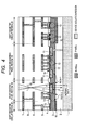
- Fig. 4 shows a cross sectional structure having no anti-crosstalk DNW 9 (corresponding to Fig. 1 .
- Components having identical references with those in Fig. 1 show that they have identical configuration as those in Fig. 1 ) and photocharge transfer paths when light 50 is incident on the photometric pixel region 18.
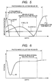
- Fig. 5 shows an impurity profile in the direction Y-Y' in the photodiode PD in Fig. 4
- Fig. 6 shows a potential diagram in the impurity profile shown in Fig. 5 .
- a region over the P + Si conductor substrate 1 functions as a photocharge collection region 36.
- an impurity profile 30 for the P type protective layer 11 There are shown an impurity profile 30 for the P type protective layer 11, an impurity profile 31 for the N type photodiode 10, an impurity profile 32 for the P well 12, an impurity profile 33 for the P - Si layer 2, and an impurity profile 34 for the P + Si semiconductor substrate 1.
- a region 35 of a weak internal electric field comprising the P well 12, the P - Si layer 2, and the P + Si semiconductor substrate 1 is formed.
- Fig. 7 shows the state.
- the potential is minimum at 60 in the N type impurity region forming the photodiode PC, no sufficient potential gradient can be ensured in a region 35 of weak internal electric field.
- photocharges reaching the deep region of the sensor device cannot be transferred efficiently to the region 60 of the photodiode PD. That is, since the potential gradient in the longitudinal direction of the device is weak, photocharges are diffused laterally before reaching the photodiode PD.
- the light 50 incident on the photometric pixel region causes crosstalk to the distance measuring pixel region 19 as shown by the path 1 in Fig. 4 , in which the photosensitivity of the photometric pixel 18 is lowered, and photocharges are observed as false signals in the distance measuring pixel 19.
- a portion of the photocharges generated by the incident light 50 causes crosstalk to the shift resistor circuit 20 as shown by the path 2 in Fig. 4 in which the photosensitivity of the light measuring element 18 is also lowered.
- Fig. 7 shows the photocharge transfer path when the light 50 is incident on the photometric pixel 18 in Fig. 1
- Fig. 8 shows an impurity profile in the direction Z-Z' in an anti-crosstalk layer DNW 9a disposed to the photodiode PD in Fig. 7
- Fig. 9 shows a potential diagram in the impurity profile shown in Fig. 8 .
- a region over the P + Si semiconductor substrate 1 functions as a photocharge collection region 85.
- an impurity profile 80 of the P type surface protective layer 11 There are shown an impurity profile 80 of the P type surface protective layer 11, an impurity profile 81 of the N type photodiode 10, an impurity profile 82 of the P well 12, an impurity profile 83 of the P - Si layer 2, an impurity profile 84 of a P + Si semiconductor substrate 1, and an impurity profile 87 of the anti-crosstalk layer DNW 9.
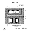
- Fig. 10 is an upper plan view for a main portion of a photometric pixel region 18 and a distance measuring pixel region 19 corresponding to the region shown as the region A in Fig. 2 (cross section along K-K' shown in Fig. 11) and Fig. 11 shows a cross sectional structure along A-A' in Fig. 10 .
- the as pillar shape anti-crosstalk layer DNW 9 the impurity profile shown in Fig.
- the N well DNWa 101 in the deep region is disposed as a ring-shape in the pixel boundary region and in each of the pixels.
- an N well 103 is arranged over the N well DNWa 101b in the deep region of the pixel boundary 100 so as to apply a potential that absorbs photocharges causing crosstalk.
- the N wells DNWa 101b in the deep region of the pixel boundary region are connected to each other although not illustrated and applied with a positive voltage by way of an impurity region 13 and the N well 103 as the power supply region. For example, a positive voltage identical with a power source voltage is applied to the N well DNWa 101b in the deep region of the pixel boundary region by way of the power supply region to absorb photocharges having a negative potential.
- an N well DNWb 102 in the shallow region are formed as a dot shape over the N well DNWa 101ea in the deep region arranged in the ring shape to the photometric pixel 18 and the distance measuring pixel 19.
- the N well DNWb 102a in the shallow region is connected to the photodiode PD 10 and transfers the photocharges generated in the pixel to the photodiode PD.
- the potential of the N well DNWa 101a in the deep region is formed at a position between the P + Si semiconductor substrate 1 and the P well 12, and the potential can be designed by utilizing the direction of the depth in Fig. 11 . That is, since the PNP junction is formed in the vertical direction (direction Z) by the N well DNWa 101a in the deep region sandwiched between the P + Si semiconductor substrate 1 and the P well 12, it is possible to control the potential of the N well DNWa 101a in the deep region and design the potential gradient so as to decrease from the deep region of the N well DNWa 101a to the photodiode 10.
- the N well DNWa 101a in the deep region is arranged as the ring shape, since the electric field effect in the directions X and Y in Fig. 11 can be utilized (that is, PNP junction is formed also in the direction X or the direction Y by forming the DNW as the ring shape), the N well DNWa 101a in the deep region can be depleted at a high potential to facilitate the potential design.
- the N well DNWb 102 in the shallow region is formed at the position near the deep region of the P well 12, and the potential is designed so as to attain depletion by using the PN junction of the P well 12 and the N well DNWb 102 in the shallow region.
- the N well DNWb 102 in the shallow region is formed such that the density is slightly increased along the impurity distribution of the P well 12.
- depletion can be attained by utilizing the electric field effect from the directions X and Y in Fig. 11 to facilitate the potential design.
- the N well DNWa 101 in the deep region and the N well DNWb 102 in the shallow region are arranged at the outermost periphery of each of the pixels. With such an arrangement, it is possible to collect photocharges generated by the light incident into the pixels over a wide range and improve the sensitivity.
- the photosensitivity was improved by 1.7 times, and the crosstalk between the photometric pixel and the distance measuring pixel and the crosstalk between the distance measuring pixel and the distance measuring pixel were improved by -20 dB or more.
- Fig. 12 shows the crosstalk effect between the distance measuring pixel and the distance measuring pixel when this embodiment is applied.
- An improvement of -20 dB or more was obtained in a region at wavelength from 500 nm to 800 nm that corresponds to a visible light.
- Fig. 13 is an upper plan view of a main portion of a photometric pixel region 18 and a distance measuring pixel region 19 corresponding to a region shown as the region A in Fig. 2 (cross section along K-K' shown in Fig. 14) and Fig. 14 shows a cross sectional structure along A-A' in Fig. 13 .
- the second embodiment has a feature that the N well DNWa 101 in the deep region in the photometric pixel 18 and the distance measuring pixel 19 are arranged as a planar shape over the entire region in respective pixels, and dot-shaped N well DNWb 102 in the shallow region are arranged over the entire region in the pixel.
- photocharges generated in the deep region in the pixel are transferred by way of the N well DNWa 101 in the deep region and the N well DNWb 102 in the shallow region to the photodiode 10 in the same manner as in the first embodiment.
- the number of the paths for transferring the photocharges by way of the N well DNWa 101 in the deep region and the N well DNWb 102 in the shallow region to the photodiode PD can be increased compared with the first embodiment, and charges can be transferred at a higher speed and at a higher efficiency.
- the charge store region (N type) of the well DNWa 101 in the deep region, the N well 102 in the shallow region, and the photodiode 10 can be increased, the amount of storable signal charges can be increased.
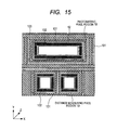
- Fig. 15 is an upper plan view for a main portion of a photometric pixel region 18 and a distance measuring pixel region 19 corresponding to a region shown as the region A in Fig. 2 (corresponding to the cross section along K-K' shown in Fig. 11 ).
- this embodiment has a feature that the N well DNWb 102 in the shallow region is formed as a line shape at the outer periphery in the pixel.
- photocharges generated in the deep region in the pixel are transferred by way of the N well DNWa 101 in the deep region and the N well DNWb 102 in the shallow region to the photodiode 10 in the same manner as in the first embodiment.
- the N well DNWb 102 in the shallow region is formed as the line shape, the photocharges generated in the pixel can be absorbed to the N well DNW without escaping them to the outside of the pixel region, and the photosensitivity is improved.
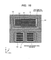
- Fig. 16 is an upper plan view for a main portion of a photometric pixel region 18 and a distance measuring pixel region 19 corresponding to a region shown as the region A in Fig. 2 corresponding to this modified embodiment (corresponding to the cross section along K-K' shown in Fig. 11 ).
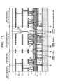
- Fig. 17 is a view showing another cross sectional structure for a main portion of a solid-state imaging apparatus of the invention. It has a feature that an anti-crosstalk layer DNW 110 (N well in the deep region) is arranged below a transistors forming the photometric pixel and the distance measuring pixel in addition to those of the first embodiment.
- an anti-crosstalk layer DNW 110 N well in the deep region
- the invention is also applicable to other solid-state imaging devices, for example, a CCD image sensor.
Landscapes
- Solid State Image Pick-Up Elements (AREA)
- Element Separation (AREA)
Applications Claiming Priority (1)
| Application Number | Priority Date | Filing Date | Title |
|---|---|---|---|
| JP2011185464A JP5677238B2 (ja) | 2011-08-29 | 2011-08-29 | 固体撮像装置 |
Publications (2)
| Publication Number | Publication Date |
|---|---|
| EP2565925A2 true EP2565925A2 (de) | 2013-03-06 |
| EP2565925A3 EP2565925A3 (de) | 2014-05-07 |
Family
ID=46465007
Family Applications (1)
| Application Number | Title | Priority Date | Filing Date |
|---|---|---|---|
| EP12004985.3A Withdrawn EP2565925A3 (de) | 2011-08-29 | 2012-07-05 | Festkörperabbildungsvorrichtung |
Country Status (5)
| Country | Link |
|---|---|
| US (1) | US9093349B2 (de) |
| EP (1) | EP2565925A3 (de) |
| JP (1) | JP5677238B2 (de) |
| KR (1) | KR101373905B1 (de) |
| TW (1) | TWI483391B (de) |
Cited By (2)
| Publication number | Priority date | Publication date | Assignee | Title |
|---|---|---|---|---|
| EP2866260A3 (de) * | 2013-10-07 | 2015-08-26 | Canon Kabushiki Kaisha | Festkörperbildgebungsvorrichtung, Verfahren zur Herstellung davon und Bildgebungssystem |
| EP3067931A1 (de) * | 2015-03-11 | 2016-09-14 | Canon Kabushiki Kaisha | Pixel, festkörperbildgebungsvorrichtung und bildgebungsvorrichtung |
Families Citing this family (5)
| Publication number | Priority date | Publication date | Assignee | Title |
|---|---|---|---|---|
| JP6115982B2 (ja) * | 2011-07-04 | 2017-04-19 | ソニーセミコンダクタソリューションズ株式会社 | 撮像素子および撮像装置 |
| JP2016092178A (ja) | 2014-11-04 | 2016-05-23 | 株式会社リコー | 固体撮像素子 |
| KR102577844B1 (ko) | 2016-08-09 | 2023-09-15 | 삼성전자주식회사 | 이미지 센서 |
| US10410934B2 (en) * | 2017-12-07 | 2019-09-10 | Micron Technology, Inc. | Apparatuses having an interconnect extending from an upper conductive structure, through a hole in another conductive structure, and to an underlying structure |
| KR20220034973A (ko) * | 2020-09-11 | 2022-03-21 | 삼성전자주식회사 | 이미지 센서 |
Citations (3)
| Publication number | Priority date | Publication date | Assignee | Title |
|---|---|---|---|---|
| JP2004031878A (ja) | 2002-06-28 | 2004-01-29 | Fuji Film Microdevices Co Ltd | 固体撮像装置 |
| JP2006024907A (ja) | 2004-06-07 | 2006-01-26 | Canon Inc | 固体撮像装置 |
| JP2006064956A (ja) | 2004-08-26 | 2006-03-09 | Canon Inc | オートフォーカス用固体撮像装置とそれを用いたオートフォーカスカメラ |
Family Cites Families (11)
| Publication number | Priority date | Publication date | Assignee | Title |
|---|---|---|---|---|
| JP2002164529A (ja) * | 2000-11-28 | 2002-06-07 | Sony Corp | 固体撮像素子およびその製造方法 |
| JP4270742B2 (ja) * | 2000-11-30 | 2009-06-03 | Necエレクトロニクス株式会社 | 固体撮像装置 |
| KR100461975B1 (ko) * | 2002-12-27 | 2004-12-17 | 매그나칩 반도체 유한회사 | 이미지센서의 트렌치 소자분리막 형성방법 |
| JP4426273B2 (ja) * | 2003-05-22 | 2010-03-03 | イノテック株式会社 | Mos型固体撮像装置及びその製造方法 |
| JP4530747B2 (ja) | 2004-07-16 | 2010-08-25 | 富士通セミコンダクター株式会社 | 固体撮像装置及びその製造方法 |
| JP4595464B2 (ja) * | 2004-09-22 | 2010-12-08 | ソニー株式会社 | Cmos固体撮像素子の製造方法 |
| KR100924706B1 (ko) * | 2005-03-28 | 2009-11-03 | 후지쯔 마이크로일렉트로닉스 가부시키가이샤 | 촬상 장치 |
| KR20080016259A (ko) * | 2006-08-18 | 2008-02-21 | 동부일렉트로닉스 주식회사 | 씨모스 이미지 센서 및 그 제조방법 |
| US8357984B2 (en) * | 2008-02-08 | 2013-01-22 | Omnivision Technologies, Inc. | Image sensor with low electrical cross-talk |
| JP5328207B2 (ja) * | 2008-04-01 | 2013-10-30 | キヤノン株式会社 | 固体撮像装置 |
| KR101534544B1 (ko) * | 2008-09-17 | 2015-07-08 | 삼성전자주식회사 | 에피 층을 갖는 픽셀 셀을 구비한 이미지 센서, 이를 포함하는 시스템, 및 픽셀 셀 형성 방법 |
-
2011
- 2011-08-29 JP JP2011185464A patent/JP5677238B2/ja not_active Expired - Fee Related
-
2012
- 2012-06-21 TW TW101122195A patent/TWI483391B/zh not_active IP Right Cessation
- 2012-07-05 EP EP12004985.3A patent/EP2565925A3/de not_active Withdrawn
- 2012-07-11 KR KR1020120075784A patent/KR101373905B1/ko not_active Expired - Fee Related
- 2012-07-12 US US13/547,452 patent/US9093349B2/en not_active Expired - Fee Related
Patent Citations (3)
| Publication number | Priority date | Publication date | Assignee | Title |
|---|---|---|---|---|
| JP2004031878A (ja) | 2002-06-28 | 2004-01-29 | Fuji Film Microdevices Co Ltd | 固体撮像装置 |
| JP2006024907A (ja) | 2004-06-07 | 2006-01-26 | Canon Inc | 固体撮像装置 |
| JP2006064956A (ja) | 2004-08-26 | 2006-03-09 | Canon Inc | オートフォーカス用固体撮像装置とそれを用いたオートフォーカスカメラ |
Cited By (7)
| Publication number | Priority date | Publication date | Assignee | Title |
|---|---|---|---|---|
| EP2866260A3 (de) * | 2013-10-07 | 2015-08-26 | Canon Kabushiki Kaisha | Festkörperbildgebungsvorrichtung, Verfahren zur Herstellung davon und Bildgebungssystem |
| RU2589519C2 (ru) * | 2013-10-07 | 2016-07-10 | Кэнон Кабусики Кайся | Твердотельное устройство формирования изображения, способ изготовления этого устройства и система формирования изображения |
| US9761618B2 (en) | 2013-10-07 | 2017-09-12 | Canon Kabushiki Kaisha | Solid-state imaging apparatus, method for manufacturing the same, and imaging system |
| US9947702B2 (en) | 2013-10-07 | 2018-04-17 | Canon Kabushiki Kaisha | Solid-state imaging apparatus, method for manufacturing the same, and imaging system |
| US10217780B2 (en) | 2013-10-07 | 2019-02-26 | Canon Kabushiki Kaisha | Solid-state imaging apparatus, method for manufacturing the same, and imaging system |
| EP3067931A1 (de) * | 2015-03-11 | 2016-09-14 | Canon Kabushiki Kaisha | Pixel, festkörperbildgebungsvorrichtung und bildgebungsvorrichtung |
| US9998691B2 (en) | 2015-03-11 | 2018-06-12 | Canon Kabushiki Kaisha | Pixel, a solid-state imaging device, and an imaging apparatus having barrier region between photoelectric conversion portions in parallel |
Also Published As
| Publication number | Publication date |
|---|---|
| TW201314877A (zh) | 2013-04-01 |
| JP5677238B2 (ja) | 2015-02-25 |
| KR101373905B1 (ko) | 2014-03-12 |
| EP2565925A3 (de) | 2014-05-07 |
| US9093349B2 (en) | 2015-07-28 |
| KR20130024740A (ko) | 2013-03-08 |
| JP2013048132A (ja) | 2013-03-07 |
| US20130049156A1 (en) | 2013-02-28 |
| TWI483391B (zh) | 2015-05-01 |
Similar Documents
| Publication | Publication Date | Title |
|---|---|---|
| KR102577844B1 (ko) | 이미지 센서 | |
| US8835981B2 (en) | Solid-state image sensor | |
| US8597972B2 (en) | Back-illuminated type solid-state imaging device | |
| TWI740958B (zh) | 用於前照式紅外線影像感測器的光電閘及其製造方法 | |
| US8564701B2 (en) | Solid-state imaging device having a buried photodiode and a buried floating diffusion positioned for improved signal charge transfer, and electronic apparatus including the solid-state imaging device | |
| US8916917B2 (en) | Solid-state imaging device | |
| KR101458052B1 (ko) | 혼색 방지 구조를 갖는 시모스 이미지 센서 및 그 제조방법 | |
| US9093349B2 (en) | Solid-state imaging apparatus | |
| US20160218138A1 (en) | Solid-state image pickup device and method for manufacturing a solid-state image pickup device | |
| JP2023017991A (ja) | 撮像素子 | |
| JP4751865B2 (ja) | 裏面照射型固体撮像素子及びその製造方法 | |
| US9865631B2 (en) | Solid-state image pickup apparatus | |
| KR20170043140A (ko) | 이미지 센서 | |
| CN103579274B (zh) | 图像拾取装置和图像拾取系统 | |
| JP2008172005A (ja) | 固体撮像装置、電子モジュール及び電子機器 | |
| US8462239B2 (en) | Solid-state imaging device and electronic imaging device having multi-stage element isolation layer | |
| US12219284B2 (en) | Solid-state imaging device | |
| JP4987749B2 (ja) | 固体撮像素子の製造方法 | |
| JP2018067615A (ja) | 固体撮像装置及びその製造方法、並びに、電子機器 | |
| JP5534081B2 (ja) | 固体撮像素子の製造方法 | |
| JP2012142623A (ja) | 固体撮像素子の製造方法および固体撮像素子 | |
| JP2018046089A (ja) | 固体撮像装置及びその製造方法、並びに、電子機器 | |
| JP5252100B2 (ja) | 固体撮像素子 | |
| KR20240167171A (ko) | 이미지 센서 및 그의 제조 방법 | |
| KR20240095209A (ko) | 광 검출 장치 및 전자 기기 |
Legal Events
| Date | Code | Title | Description |
|---|---|---|---|
| PUAI | Public reference made under article 153(3) epc to a published international application that has entered the european phase |
Free format text: ORIGINAL CODE: 0009012 |
|
| 17P | Request for examination filed |
Effective date: 20121031 |
|
| AK | Designated contracting states |
Kind code of ref document: A2 Designated state(s): AL AT BE BG CH CY CZ DE DK EE ES FI FR GB GR HR HU IE IS IT LI LT LU LV MC MK MT NL NO PL PT RO RS SE SI SK SM TR |
|
| AX | Request for extension of the european patent |
Extension state: BA ME |
|
| PUAL | Search report despatched |
Free format text: ORIGINAL CODE: 0009013 |
|
| AK | Designated contracting states |
Kind code of ref document: A3 Designated state(s): AL AT BE BG CH CY CZ DE DK EE ES FI FR GB GR HR HU IE IS IT LI LT LU LV MC MK MT NL NO PL PT RO RS SE SI SK SM TR |
|
| AX | Request for extension of the european patent |
Extension state: BA ME |
|
| RBV | Designated contracting states (corrected) |
Designated state(s): AL AT BE BG CH CY CZ DE DK EE ES FI FR GB GR HR HU IE IS IT LI LT LU LV MC MK MT NL NO PL PT RO RS SE SI SK SM TR |
|
| RIC1 | Information provided on ipc code assigned before grant |
Ipc: H01L 27/146 20060101AFI20140403BHEP |
|
| 17Q | First examination report despatched |
Effective date: 20150703 |
|
| STAA | Information on the status of an ep patent application or granted ep patent |
Free format text: STATUS: EXAMINATION IS IN PROGRESS |
|
| STAA | Information on the status of an ep patent application or granted ep patent |
Free format text: STATUS: THE APPLICATION IS DEEMED TO BE WITHDRAWN |
|
| 18D | Application deemed to be withdrawn |
Effective date: 20180201 |