EP2565931A1 - MOS Transistor - Google Patents
MOS Transistor Download PDFInfo
- Publication number
- EP2565931A1 EP2565931A1 EP12194669A EP12194669A EP2565931A1 EP 2565931 A1 EP2565931 A1 EP 2565931A1 EP 12194669 A EP12194669 A EP 12194669A EP 12194669 A EP12194669 A EP 12194669A EP 2565931 A1 EP2565931 A1 EP 2565931A1
- Authority
- EP
- European Patent Office
- Prior art keywords
- layer
- epi
- gate
- gate electrode
- drain
- Prior art date
- Legal status (The legal status is an assumption and is not a legal conclusion. Google has not performed a legal analysis and makes no representation as to the accuracy of the status listed.)
- Withdrawn
Links
Images
Classifications
-
- H—ELECTRICITY
- H10—SEMICONDUCTOR DEVICES; ELECTRIC SOLID-STATE DEVICES NOT OTHERWISE PROVIDED FOR
- H10P—GENERIC PROCESSES OR APPARATUS FOR THE MANUFACTURE OR TREATMENT OF DEVICES COVERED BY CLASS H10
- H10P10/00—Bonding of wafers, substrates or parts of devices
-
- H—ELECTRICITY
- H10—SEMICONDUCTOR DEVICES; ELECTRIC SOLID-STATE DEVICES NOT OTHERWISE PROVIDED FOR
- H10D—INORGANIC ELECTRIC SEMICONDUCTOR DEVICES
- H10D30/00—Field-effect transistors [FET]
- H10D30/01—Manufacture or treatment
- H10D30/021—Manufacture or treatment of FETs having insulated gates [IGFET]
- H10D30/027—Manufacture or treatment of FETs having insulated gates [IGFET] of lateral single-gate IGFETs
- H10D30/0275—Manufacture or treatment of FETs having insulated gates [IGFET] of lateral single-gate IGFETs forming single crystalline semiconductor source or drain regions resulting in recessed gates, e.g. forming raised source or drain regions
-
- H—ELECTRICITY
- H10—SEMICONDUCTOR DEVICES; ELECTRIC SOLID-STATE DEVICES NOT OTHERWISE PROVIDED FOR
- H10D—INORGANIC ELECTRIC SEMICONDUCTOR DEVICES
- H10D30/00—Field-effect transistors [FET]
- H10D30/60—Insulated-gate field-effect transistors [IGFET]
- H10D30/601—Insulated-gate field-effect transistors [IGFET] having lightly-doped drain or source extensions, e.g. LDD IGFETs or DDD IGFETs
- H10D30/608—Insulated-gate field-effect transistors [IGFET] having lightly-doped drain or source extensions, e.g. LDD IGFETs or DDD IGFETs having non-planar bodies, e.g. having recessed gate electrodes
-
- H—ELECTRICITY
- H10—SEMICONDUCTOR DEVICES; ELECTRIC SOLID-STATE DEVICES NOT OTHERWISE PROVIDED FOR
- H10D—INORGANIC ELECTRIC SEMICONDUCTOR DEVICES
- H10D64/00—Electrodes of devices having potential barriers
- H10D64/01—Manufacture or treatment
- H10D64/021—Manufacture or treatment using multiple gate spacer layers, e.g. bilayered sidewall spacers
-
- H—ELECTRICITY
- H10—SEMICONDUCTOR DEVICES; ELECTRIC SOLID-STATE DEVICES NOT OTHERWISE PROVIDED FOR
- H10D—INORGANIC ELECTRIC SEMICONDUCTOR DEVICES
- H10D64/00—Electrodes of devices having potential barriers
- H10D64/20—Electrodes characterised by their shapes, relative sizes or dispositions
- H10D64/27—Electrodes not carrying the current to be rectified, amplified, oscillated or switched, e.g. gates
- H10D64/311—Gate electrodes for field-effect devices
- H10D64/411—Gate electrodes for field-effect devices for FETs
- H10D64/511—Gate electrodes for field-effect devices for FETs for IGFETs
- H10D64/517—Gate electrodes for field-effect devices for FETs for IGFETs characterised by the conducting layers
- H10D64/518—Gate electrodes for field-effect devices for FETs for IGFETs characterised by the conducting layers characterised by their lengths or sectional shapes
-
- H—ELECTRICITY
- H10—SEMICONDUCTOR DEVICES; ELECTRIC SOLID-STATE DEVICES NOT OTHERWISE PROVIDED FOR
- H10D—INORGANIC ELECTRIC SEMICONDUCTOR DEVICES
- H10D30/00—Field-effect transistors [FET]
- H10D30/01—Manufacture or treatment
- H10D30/021—Manufacture or treatment of FETs having insulated gates [IGFET]
- H10D30/0212—Manufacture or treatment of FETs having insulated gates [IGFET] using self-aligned silicidation
Definitions
- the invention is related to a metal-oxide-semiconductor (MOS) transistor having an elevated source/drain structure.
- MOS metal-oxide-semiconductor
- FET Field Effect Transistors
- a shallow junction source/drain structure has been developed.
- a source and a drain are constructed in the form of an LDD (Lightly Doped Drain) structure to suppress the short channel effect.
- LDD Lightly Doped Drain
- Such an LDD structure is limited in use, since it can be applied to only a semiconductor element with a gate line width of 0.35 ⁇ m or larger to suppress the short channel effect, and cannot be applied to a semiconductor element with a gate line width of 0.35 ⁇ m or less. This is because there is a limit to the extent to which the depth of the junction can be reduced, and thus formation of a junction in the LDD structure is impractical or impossible.
- US 6,445,042 B1 discloses a method of fabricating a MOS transistor having an elevated source/drain structure, where a gate dielectric is formed on an active region of a semiconductor substrate, a gate electrode is formed on the gate dielectric, a first gate spacer is formed on lateral side surfaces of the gate electrode, a first epi-layer is formed on the semiconductor substrate, a second gate spacer is formed on lateral side surfaces of the first gate spacer, and a second epi-layer is formed on the first epi-layer.
- a source/drain extension region is formed by a dopant implantation before forming the first epi-layer or, in an alternative embodiment, after forming the second epi-layer.
- US 6,326,664 B1 discloses to form a source/drain extension region of a MOS transistor by an out-diffusion process after having formed a doped first semiconductor layer, where dopants diffuse out of said first semiconductor layer into an underlying region of a substrate.
- This prior art fabrication method further includes to form a silicide layer on the first semiconductor layer, and to form a deep source/drain region by implanting a dopant through the silicide layer and the first semiconductor layer.
- Other prior art MOS transistor fabrication methods including to form an elevated source/drain structure are disclosed in US 5,012,306 and US 6,022,771 .
- Typical MOS transistor gate structures may comprise a poly-layer, i.e. polysilicon layer, formed on the gate electrode, see e.g. US 2001/0034085 A1 , EP 0 480 446 A2 , US 6,277,677 B1 , and EP 0 780 907 A2 .
- MOS transistor which avoids the above-mentioned limitations of the LDD structure at least partially, and is in particular capable of preventing the short-channel effect in an advantageous manner.
- the invention provides a MOS transistor according to claim 1 that includes an elevated source/drain junction with a deep source/drain layer.
- Advantageous embodiments of the invention are further given in the subclaims, the wording of which is herewith incorporated by reference into the description for brevity sake.
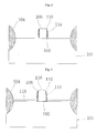
- device separators 104 are formed on a semiconductor substrate 101 to define an active area, or active region, between the separators 104.
- the semiconductor substrate 101 is composed of silicon.
- the device separators may be formed, for example, by any of the well-known techniques including the formation of field oxide structures 104 according to the local oxidation of silicon (LOCOS) process, and the shallow trench isolation (STI) method.
- LOC local oxidation of silicon
- STI shallow trench isolation
- a gate dielectric 106 is formed on the active region of the semiconductor substrate 101, for example, by a deposit of a material selected from the group consisting of SiO 2 , SiON, SiN, Al 2 O 3 , and mixtures thereof. In one embodiment, the resulting gate dielectric 106 thus formed is 20 to 100 ⁇ in thickness.
- a conductive film for a gate electrode is then deposited on the active area of the semiconductor substrate 101 on which the gate dielectric 106 is formed, and the resulting semiconductor substrate 101 is patterned to form the gate electrode 108 structure on the semiconductor substrate 101.
- the material of the conductive film is selected from the group consisting of poly-silicon (poly-Si), silicon-germanium (SiGe), and germanium (Ge), and other applicable conductive materials.
- the gate electrode 108 is subjected to an oxidation process or a chemical vapor deposition (CVD) process to form a first gate oxide 110 on lateral surfaces, or side walls, of the gate electrode 108.
- a dielectric layer such as a nitride (e.g. SiN) layer, is then formed on the semiconductor substrate 101 according to the CVD process, and the resulting semiconductor substrate 101 is etched to form a first gate spacer 114 on the first gate oxide 110.
- the gate dielectric layer other than that portion covered by a lower portion of the first gate oxide 110 surrounding the gate electrode 108 and other than that portion positioned under the first gate electrode 108 is etched in an anisotropic etching procedure, while the semiconductor substrate 101 is etched to form the first gate spacer 114.
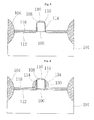
- a high-temperature hydrogen baking process using hydrogen gas is conducted so as to smoothly deposit a first epi-layer 118 on the semiconductor substrate 101 in accordance with a selective epitaxial growth (SEG) process.
- SEG selective epitaxial growth
- the SEG process is conducted in a low-pressure chemical vapor deposition (LPCVD) or a ultra-high vacuum chemical vapor deposition (UHV-CVD) procedure to form a gate silicon 116 on the gate electrode 108 and to form the first epi-layer 118 between the field oxide 104 and the first gate spacer 114.
- LPCVD low-pressure chemical vapor deposition
- UHV-CVD ultra-high vacuum chemical vapor deposition
- a dopant is implanted in a portion of the semiconductor substrate 101 under the first epi-layer 118 at a concentration of about 10 14 ions/cm 2 , for example BF 2 is ion-implanted at 3 keV in the case of PMOS (p-channel metal-oxide semiconductor) and As is ion-implanted at 10 keV in the case of NMOS (n-channel metal-oxide semiconductor) in the semiconductor substrate 101 to form a source/drain extension layer 112 in the semiconductor substrate 101.
- PMOS p-channel metal-oxide semiconductor
- NMOS n-channel metal-oxide semiconductor
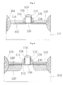
- a second gate oxide 130 is formed on the first gate spacer 114 in accordance with the CVD process.
- a dielectric such as nitride (e.g. SiN) is then deposited on the second gate oxide 130 by the CVD process so as to construct a second gate spacer 134.
- the resulting semiconductor substrate 101 is etched to form the second gate spacer 134.
- a lateral thickness ratio of the first gate spacer 114 to the second gate spacer 134 is about 1 : 5.
- the SEG process is conducted, for example using an LPCVD or UHV-CVD procedure, to form a second epi-layer 140 on the gate silicon 116 and the first epi-layer 118.
- the second epi-layer 140 is about 70 to 80 % of the resulting elevated source/drain layer, in terms of thickness. Accordingly, it is preferable that a thickness ratio of the first epi-layer 118 to the second epi-layer 140 is about 2 : 5. In the present invention, the thickness of the first epi-layer 118 is about 100 ⁇ , and that of the second epi-layer 140 is about 250 ⁇ .
- the extended gate silicon 116 is once again extended by the SEG process of FIG. 5 .
- the width of the poly-layer positioned on the gate electrode is larger than the width of the gate.
- the poly-layer 116 positioned on the gate electrode 108 includes silicon or germanium. Accordingly, when the gate silicon is extended in this manner, the gate resistance is reduced, and the device junction leakage property is improved because, owing to the extension, the gate silicide is farther away from the junctions.
- the dopant is deeply ion-implanted into a portion of the semiconductor substrate 101 positioned under the second epi-layer 140 to form deep source/drain regions 120 under the source/drain electrodes, and the resulting semiconductor substrate 101 is annealed to activate the dopant ion-implanted in the semiconductor substrate 101.
- the silicon epi-layer may be grown under deposition conditions with a pressure of about 10 to 30 torr and a temperature of about 850 °C using a source gas consisting of dichlorosilane (DCS) and HCl in accordance with the LPCVD process. It is preferable to grow the silicon epi-layer at deposition pressure of about 20 torr.
- DCS dichlorosilane
- HCl HCl
- the silicon epi-layer may be grown under deposition conditions of a pressure of about 10 -4 to 10 -5 torr and a temperature of about 600 to 700 °C using a source gas consisting of Si 2 H 6 in accordance with the UHV-CVD process.
- the silicon-germanium epi-layer may be grown under deposition conditions with a pressure of about 20 torr and a temperature of about 650 to 750 °C using a source gas consisting of dichlorosilane (DCS), HCl, and GeH 4 in accordance with the LPCVD process.
- a source gas consisting of dichlorosilane (DCS), HCl, and GeH 4 in accordance with the LPCVD process.
- the silicon-germanium epi-layer may be grown under deposition conditions with a pressure of about 10 -4 to 10 -5 torr and a temperature of about 550 to 600 °C using a source gas consisting of dichlorosilane (DCS), HCl, and GeH 4 in accordance with the UHV-CVD process.
- a source gas consisting of dichlorosilane (DCS), HCl, and GeH 4 in accordance with the UHV-CVD process.
- the dopant content in the first or second epi-layer 118 or 140 may be controlled to 10 20 ions/cm 2 or more by in-situ doping the dopant, such as boron, phosphorous, arsenic, indium, or antimony, while growing the first or second epi-layer 118 or 140 according to the SEG process. Additionally, the dopant may be implanted into the first or second epi-layer by well-known techniques. In the case of an NMOS device, As or P is implanted at 40 keV into the first or second epi-layer, and B is implanted at 3keV into the first or second epi-layer in the case of a PMOS device.
- the present invention provides a MOS transistor with an elevated source/drain structure in accordance with a selective epitaxial growth (SEG) process, in which a source/drain extension junction is formed after an epi-layer is formed, thereby preventing the short channel effect which otherwise would have been caused by the diffusion of the source/drain junctions; leakage current is therefore reduced.
- SEG selective epitaxial growth
- the configuration of the present invention is advantageous in that the source/drain extension junctions are partially overlapped by a lower portion of the gate structure, because two lateral gate spacers are formed and two elevated source/drain layers are formed in accordance with the selective epitaxial growth process, thereby preventing the short channel effect and, at the same time, reducing sheet resistance of the source/drain layer and the gate layer.
Landscapes
- Insulated Gate Type Field-Effect Transistor (AREA)
Applications Claiming Priority (2)
| Application Number | Priority Date | Filing Date | Title |
|---|---|---|---|
| KR1020030030614A KR100621546B1 (ko) | 2003-05-14 | 2003-05-14 | 엘리베이티드 소오스/드레인 구조의 모스트랜지스터 및 그제조방법 |
| EP04009363.5A EP1478029B1 (de) | 2003-05-14 | 2004-04-21 | Verfahren zur Herstellung eines MOS-Transistors |
Related Parent Applications (2)
| Application Number | Title | Priority Date | Filing Date |
|---|---|---|---|
| EP04009363.5A Division-Into EP1478029B1 (de) | 2003-05-14 | 2004-04-21 | Verfahren zur Herstellung eines MOS-Transistors |
| EP04009363.5 Division | 2004-04-21 |
Publications (1)
| Publication Number | Publication Date |
|---|---|
| EP2565931A1 true EP2565931A1 (de) | 2013-03-06 |
Family
ID=36695818
Family Applications (2)
| Application Number | Title | Priority Date | Filing Date |
|---|---|---|---|
| EP04009363.5A Expired - Lifetime EP1478029B1 (de) | 2003-05-14 | 2004-04-21 | Verfahren zur Herstellung eines MOS-Transistors |
| EP12194669A Withdrawn EP2565931A1 (de) | 2003-05-14 | 2004-04-21 | MOS Transistor |
Family Applications Before (1)
| Application Number | Title | Priority Date | Filing Date |
|---|---|---|---|
| EP04009363.5A Expired - Lifetime EP1478029B1 (de) | 2003-05-14 | 2004-04-21 | Verfahren zur Herstellung eines MOS-Transistors |
Country Status (4)
| Country | Link |
|---|---|
| US (2) | US7033895B2 (de) |
| EP (2) | EP1478029B1 (de) |
| KR (1) | KR100621546B1 (de) |
| CN (1) | CN100456439C (de) |
Families Citing this family (51)
| Publication number | Priority date | Publication date | Assignee | Title |
|---|---|---|---|---|
| ATE470324T1 (de) * | 2003-11-12 | 2010-06-15 | Interdigital Tech Corp | System für autonomen anwendungsserver-zugriff üebr verschiedene arten von zugriffstechnologienetzwerken hinweg |
| KR101146233B1 (ko) * | 2005-06-30 | 2012-05-17 | 매그나칩 반도체 유한회사 | 반도체 장치의 제조방법 |
| KR100632465B1 (ko) | 2005-07-26 | 2006-10-09 | 삼성전자주식회사 | 반도체 소자 및 이의 제조 방법 |
| KR100721661B1 (ko) * | 2005-08-26 | 2007-05-23 | 매그나칩 반도체 유한회사 | 이미지 센서 및 그 제조 방법 |
| KR100748342B1 (ko) | 2005-09-14 | 2007-08-09 | 매그나칩 반도체 유한회사 | 씨모스 이미지 센서의 제조방법 |
| KR100725455B1 (ko) | 2005-12-12 | 2007-06-07 | 삼성전자주식회사 | 엘리베이티드 소스/드레인을 갖는 반도체 메모리 소자의 제조 방법 |
| TWI298179B (en) * | 2006-05-19 | 2008-06-21 | Promos Technologies Inc | Metal oxide semiconductor transistor and method of manufacturing thereof |
| WO2008015211A1 (en) * | 2006-08-01 | 2008-02-07 | Koninklijke Philips Electronics N.V. | Effecting selectivity of silicon or silicon-germanium deposition on a silicon or silicon-germanium substrate by doping |
| US7538387B2 (en) * | 2006-12-29 | 2009-05-26 | Taiwan Semiconductor Manufacturing Company, Ltd. | Stack SiGe for short channel improvement |
| JP5157259B2 (ja) | 2007-05-29 | 2013-03-06 | ソニー株式会社 | 固体撮像素子及び撮像装置 |
| CN101796632A (zh) | 2007-09-05 | 2010-08-04 | Nxp股份有限公司 | 晶体管及其制造方法 |
| US8420460B2 (en) | 2008-03-26 | 2013-04-16 | International Business Machines Corporation | Method, structure and design structure for customizing history effects of SOI circuits |
| US8410554B2 (en) * | 2008-03-26 | 2013-04-02 | International Business Machines Corporation | Method, structure and design structure for customizing history effects of SOI circuits |
| US20090278170A1 (en) * | 2008-05-07 | 2009-11-12 | Yun-Chi Yang | Semiconductor device and manufacturing method thereof |
| US8466502B2 (en) | 2011-03-24 | 2013-06-18 | United Microelectronics Corp. | Metal-gate CMOS device |
| US8445363B2 (en) | 2011-04-21 | 2013-05-21 | United Microelectronics Corp. | Method of fabricating an epitaxial layer |
| US8324059B2 (en) | 2011-04-25 | 2012-12-04 | United Microelectronics Corp. | Method of fabricating a semiconductor structure |
| US8426284B2 (en) | 2011-05-11 | 2013-04-23 | United Microelectronics Corp. | Manufacturing method for semiconductor structure |
| US8481391B2 (en) | 2011-05-18 | 2013-07-09 | United Microelectronics Corp. | Process for manufacturing stress-providing structure and semiconductor device with such stress-providing structure |
| US8431460B2 (en) | 2011-05-27 | 2013-04-30 | United Microelectronics Corp. | Method for fabricating semiconductor device |
| US8716750B2 (en) | 2011-07-25 | 2014-05-06 | United Microelectronics Corp. | Semiconductor device having epitaxial structures |
| US8575043B2 (en) | 2011-07-26 | 2013-11-05 | United Microelectronics Corp. | Semiconductor device and manufacturing method thereof |
| CN102931235B (zh) * | 2011-08-12 | 2016-02-17 | 中芯国际集成电路制造(上海)有限公司 | Mos晶体管及其制造方法 |
| US8647941B2 (en) | 2011-08-17 | 2014-02-11 | United Microelectronics Corp. | Method of forming semiconductor device |
| US8674433B2 (en) | 2011-08-24 | 2014-03-18 | United Microelectronics Corp. | Semiconductor process |
| US8927374B2 (en) | 2011-10-04 | 2015-01-06 | Taiwan Semiconductor Manufacturing Company, Ltd. | Semiconductor device and fabrication method thereof |
| US8476169B2 (en) | 2011-10-17 | 2013-07-02 | United Microelectronics Corp. | Method of making strained silicon channel semiconductor structure |
| US8691659B2 (en) | 2011-10-26 | 2014-04-08 | United Microelectronics Corp. | Method for forming void-free dielectric layer |
| US8754448B2 (en) | 2011-11-01 | 2014-06-17 | United Microelectronics Corp. | Semiconductor device having epitaxial layer |
| US8647953B2 (en) | 2011-11-17 | 2014-02-11 | United Microelectronics Corp. | Method for fabricating first and second epitaxial cap layers |
| US8709930B2 (en) | 2011-11-25 | 2014-04-29 | United Microelectronics Corp. | Semiconductor process |
| US9136348B2 (en) | 2012-03-12 | 2015-09-15 | United Microelectronics Corp. | Semiconductor structure and fabrication method thereof |
| US9202914B2 (en) | 2012-03-14 | 2015-12-01 | United Microelectronics Corporation | Semiconductor device and method for fabricating the same |
| US8664069B2 (en) | 2012-04-05 | 2014-03-04 | United Microelectronics Corp. | Semiconductor structure and process thereof |
| US8866230B2 (en) | 2012-04-26 | 2014-10-21 | United Microelectronics Corp. | Semiconductor devices |
| US8835243B2 (en) | 2012-05-04 | 2014-09-16 | United Microelectronics Corp. | Semiconductor process |
| US8951876B2 (en) | 2012-06-20 | 2015-02-10 | United Microelectronics Corp. | Semiconductor device and manufacturing method thereof |
| US8796695B2 (en) | 2012-06-22 | 2014-08-05 | United Microelectronics Corp. | Multi-gate field-effect transistor and process thereof |
| US8710632B2 (en) | 2012-09-07 | 2014-04-29 | United Microelectronics Corp. | Compound semiconductor epitaxial structure and method for fabricating the same |
| US9117925B2 (en) | 2013-01-31 | 2015-08-25 | United Microelectronics Corp. | Epitaxial process |
| US8753902B1 (en) | 2013-03-13 | 2014-06-17 | United Microelectronics Corp. | Method of controlling etching process for forming epitaxial structure |
| US9034705B2 (en) | 2013-03-26 | 2015-05-19 | United Microelectronics Corp. | Method of forming semiconductor device |
| US9064893B2 (en) | 2013-05-13 | 2015-06-23 | United Microelectronics Corp. | Gradient dopant of strained substrate manufacturing method of semiconductor device |
| US8853060B1 (en) | 2013-05-27 | 2014-10-07 | United Microelectronics Corp. | Epitaxial process |
| US9076652B2 (en) | 2013-05-27 | 2015-07-07 | United Microelectronics Corp. | Semiconductor process for modifying shape of recess |
| US8765546B1 (en) | 2013-06-24 | 2014-07-01 | United Microelectronics Corp. | Method for fabricating fin-shaped field-effect transistor |
| US8895396B1 (en) | 2013-07-11 | 2014-11-25 | United Microelectronics Corp. | Epitaxial Process of forming stress inducing epitaxial layers in source and drain regions of PMOS and NMOS structures |
| US8981487B2 (en) | 2013-07-31 | 2015-03-17 | United Microelectronics Corp. | Fin-shaped field-effect transistor (FinFET) |
| US9941388B2 (en) * | 2014-06-19 | 2018-04-10 | Globalfoundries Inc. | Method and structure for protecting gates during epitaxial growth |
| CN110491934A (zh) * | 2019-08-29 | 2019-11-22 | 上海华力集成电路制造有限公司 | Fdsoi-mos晶体管、电路单元及其制造方法 |
| US11935793B2 (en) * | 2020-05-29 | 2024-03-19 | Taiwan Semiconductor Manufacturing Co., Ltd. | Dual dopant source/drain regions and methods of forming same |
Citations (12)
| Publication number | Priority date | Publication date | Assignee | Title |
|---|---|---|---|---|
| US5012306A (en) | 1989-09-22 | 1991-04-30 | Board Of Regents, The University Of Texas System | Hot-carrier suppressed sub-micron MISFET device |
| EP0480446A2 (de) | 1990-10-12 | 1992-04-15 | Texas Instruments Incorporated | Verfahren zum Herstellen eines hochleistungsfähigen Feldeffekttransistors mit isoliertem Gate und danach hergestellter Transistor |
| EP0780907A2 (de) | 1995-12-21 | 1997-06-25 | Nec Corporation | Halbleiterbauelement mit flacher Verunreinigungszone ohne Kurzschluss zwischen der Gate-Elektrode und den Source/Drain-Gebieten und Verfahren zu seiner Herstellung |
| US5998248A (en) * | 1999-01-25 | 1999-12-07 | International Business Machines Corporation | Fabrication of semiconductor device having shallow junctions with tapered spacer in isolation region |
| US6022771A (en) | 1999-01-25 | 2000-02-08 | International Business Machines Corporation | Fabrication of semiconductor device having shallow junctions and sidewall spacers creating taper-shaped isolation where the source and drain regions meet the gate regions |
| US6187642B1 (en) * | 1999-06-15 | 2001-02-13 | Advanced Micro Devices Inc. | Method and apparatus for making mosfet's with elevated source/drain extensions |
| US6277677B1 (en) | 1999-04-12 | 2001-08-21 | Hyundai Electronics Industries Co., Ltd. | Method of manufacturing a semiconductor device |
| US20010034085A1 (en) | 1999-03-16 | 2001-10-25 | Kabushiki Kaisha Toshiba | Method of manufacturing a semiconductor and semiconductor device |
| US6326664B1 (en) | 1994-12-23 | 2001-12-04 | Intel Corporation | Transistor with ultra shallow tip and method of fabrication |
| US20020000611A1 (en) * | 2000-06-30 | 2002-01-03 | Kabushiki Kaisha Toshiba | Semiconductor device having a gate electrode with a sidewall insulating film and manufacturing method thereof |
| US6445042B1 (en) | 1999-06-15 | 2002-09-03 | Advanced Micro Devices, Inc. | Method and apparatus for making MOSFETs with elevated source/drain extensions |
| US20030030103A1 (en) * | 2001-08-04 | 2003-02-13 | Samsung Electronics Co., Ltd. | Structure of semiconductor device and method for manufacturing the same |
Family Cites Families (6)
| Publication number | Priority date | Publication date | Assignee | Title |
|---|---|---|---|---|
| US5093275A (en) * | 1989-09-22 | 1992-03-03 | The Board Of Regents, The University Of Texas System | Method for forming hot-carrier suppressed sub-micron MISFET device |
| US5539339A (en) * | 1994-06-15 | 1996-07-23 | U.S. Philips Corporation | Differential load stage with stepwise variable impedance, and clocked comparator comprising such a load stage |
| KR100333727B1 (ko) * | 1998-12-22 | 2002-06-20 | 박종섭 | 엘리베이티드소오스/드레인구조의모스트랜지스터제조방법 |
| US6235568B1 (en) | 1999-01-22 | 2001-05-22 | Intel Corporation | Semiconductor device having deposited silicon regions and a method of fabrication |
| US20030166323A1 (en) | 2002-03-01 | 2003-09-04 | Infineon Technologies North America Corp. | Raised extension structure for high performance cmos |
| US6683342B2 (en) * | 2002-06-19 | 2004-01-27 | United Microelectronics Corp. | Memory structure and method for manufacturing the same |
-
2003
- 2003-05-14 KR KR1020030030614A patent/KR100621546B1/ko not_active Expired - Fee Related
-
2004
- 2004-04-13 US US10/823,420 patent/US7033895B2/en not_active Expired - Lifetime
- 2004-04-21 EP EP04009363.5A patent/EP1478029B1/de not_active Expired - Lifetime
- 2004-04-21 EP EP12194669A patent/EP2565931A1/de not_active Withdrawn
- 2004-05-14 CN CNB2004100433165A patent/CN100456439C/zh not_active Expired - Lifetime
-
2006
- 2006-03-24 US US11/388,868 patent/US7368792B2/en not_active Expired - Lifetime
Patent Citations (12)
| Publication number | Priority date | Publication date | Assignee | Title |
|---|---|---|---|---|
| US5012306A (en) | 1989-09-22 | 1991-04-30 | Board Of Regents, The University Of Texas System | Hot-carrier suppressed sub-micron MISFET device |
| EP0480446A2 (de) | 1990-10-12 | 1992-04-15 | Texas Instruments Incorporated | Verfahren zum Herstellen eines hochleistungsfähigen Feldeffekttransistors mit isoliertem Gate und danach hergestellter Transistor |
| US6326664B1 (en) | 1994-12-23 | 2001-12-04 | Intel Corporation | Transistor with ultra shallow tip and method of fabrication |
| EP0780907A2 (de) | 1995-12-21 | 1997-06-25 | Nec Corporation | Halbleiterbauelement mit flacher Verunreinigungszone ohne Kurzschluss zwischen der Gate-Elektrode und den Source/Drain-Gebieten und Verfahren zu seiner Herstellung |
| US5998248A (en) * | 1999-01-25 | 1999-12-07 | International Business Machines Corporation | Fabrication of semiconductor device having shallow junctions with tapered spacer in isolation region |
| US6022771A (en) | 1999-01-25 | 2000-02-08 | International Business Machines Corporation | Fabrication of semiconductor device having shallow junctions and sidewall spacers creating taper-shaped isolation where the source and drain regions meet the gate regions |
| US20010034085A1 (en) | 1999-03-16 | 2001-10-25 | Kabushiki Kaisha Toshiba | Method of manufacturing a semiconductor and semiconductor device |
| US6277677B1 (en) | 1999-04-12 | 2001-08-21 | Hyundai Electronics Industries Co., Ltd. | Method of manufacturing a semiconductor device |
| US6187642B1 (en) * | 1999-06-15 | 2001-02-13 | Advanced Micro Devices Inc. | Method and apparatus for making mosfet's with elevated source/drain extensions |
| US6445042B1 (en) | 1999-06-15 | 2002-09-03 | Advanced Micro Devices, Inc. | Method and apparatus for making MOSFETs with elevated source/drain extensions |
| US20020000611A1 (en) * | 2000-06-30 | 2002-01-03 | Kabushiki Kaisha Toshiba | Semiconductor device having a gate electrode with a sidewall insulating film and manufacturing method thereof |
| US20030030103A1 (en) * | 2001-08-04 | 2003-02-13 | Samsung Electronics Co., Ltd. | Structure of semiconductor device and method for manufacturing the same |
Non-Patent Citations (1)
| Title |
|---|
| CHAO C-P ET AL: "LOW RESISTANCE TI OR CO SALICIDED RAISED SOURCE/DRAIN TRANSISTORS FOR SUB-0.13 MUM CMOS TECHNOLOGIES", INTERNATIONAL ELECTRON DEVICES MEETING 1997. IEDM TECHNICAL DIGEST. WASHINGTON, DC, DEC. 7 - 10, 1997; [INTERNATIONAL ELECTRON DEVICES MEETING], NEW YORK, NY : IEEE, US, 7 December 1997 (1997-12-07), pages 103 - 106, XP000855755, ISBN: 978-0-7803-4101-2, DOI: 10.1109/IEDM.1997.649474 * |
Also Published As
| Publication number | Publication date |
|---|---|
| KR100621546B1 (ko) | 2006-09-13 |
| CN100456439C (zh) | 2009-01-28 |
| EP1478029B1 (de) | 2014-04-16 |
| US7368792B2 (en) | 2008-05-06 |
| EP1478029A1 (de) | 2004-11-17 |
| US7033895B2 (en) | 2006-04-25 |
| KR20040098302A (ko) | 2004-11-20 |
| US20040227164A1 (en) | 2004-11-18 |
| US20060163558A1 (en) | 2006-07-27 |
| CN1551311A (zh) | 2004-12-01 |
Similar Documents
| Publication | Publication Date | Title |
|---|---|---|
| EP1478029B1 (de) | Verfahren zur Herstellung eines MOS-Transistors | |
| US6445042B1 (en) | Method and apparatus for making MOSFETs with elevated source/drain extensions | |
| US7538387B2 (en) | Stack SiGe for short channel improvement | |
| US8008157B2 (en) | CMOS device with raised source and drain regions | |
| US6707062B2 (en) | Transistor in a semiconductor device with an elevated channel and a source drain | |
| US6916694B2 (en) | Strained silicon-channel MOSFET using a damascene gate process | |
| US7122435B2 (en) | Methods, systems and structures for forming improved transistors | |
| US7700452B2 (en) | Strained channel transistor | |
| US7892930B2 (en) | Method to improve transistor tox using SI recessing with no additional masking steps | |
| US8318571B2 (en) | Method for forming P-type lightly doped drain region using germanium pre-amorphous treatment | |
| US6187642B1 (en) | Method and apparatus for making mosfet's with elevated source/drain extensions | |
| CN100585834C (zh) | 集成电路及其形成方法 | |
| US6083798A (en) | Method of producing a metal oxide semiconductor device with raised source/drain | |
| WO2005094299A2 (en) | Improved cmos transistors and methods of forming same | |
| US7432559B2 (en) | Silicide formation on SiGe | |
| US7504292B2 (en) | Short channel effect engineering in MOS device using epitaxially carbon-doped silicon | |
| US7994591B2 (en) | Semiconductor device and method for manufacturing the same | |
| KR100861835B1 (ko) | 듀얼 게이트 cmos형 반도체 소자의 제조 방법 | |
| US7892909B2 (en) | Polysilicon gate formation by in-situ doping | |
| US6905923B1 (en) | Offset spacer process for forming N-type transistors | |
| US20080194072A1 (en) | Polysilicon gate formation by in-situ doping | |
| US6184099B1 (en) | Low cost deep sub-micron CMOS process | |
| KR100637966B1 (ko) | 반도체 소자 및 그 제조 방법 |
Legal Events
| Date | Code | Title | Description |
|---|---|---|---|
| PUAI | Public reference made under article 153(3) epc to a published international application that has entered the european phase |
Free format text: ORIGINAL CODE: 0009012 |
|
| AC | Divisional application: reference to earlier application |
Ref document number: 1478029 Country of ref document: EP Kind code of ref document: P |
|
| AK | Designated contracting states |
Kind code of ref document: A1 Designated state(s): DE FR GB IT |
|
| RIN1 | Information on inventor provided before grant (corrected) |
Inventor name: PARK, MOON-HAN Inventor name: LEE, HO Inventor name: RHEE, HWA-SUNG Inventor name: LEE, SEUNG-HWAN Inventor name: YOO, JAE-YOON |
|
| 17P | Request for examination filed |
Effective date: 20130507 |
|
| RBV | Designated contracting states (corrected) |
Designated state(s): DE FR GB IT |
|
| 17Q | First examination report despatched |
Effective date: 20130710 |
|
| STAA | Information on the status of an ep patent application or granted ep patent |
Free format text: STATUS: THE APPLICATION IS DEEMED TO BE WITHDRAWN |
|
| 18D | Application deemed to be withdrawn |
Effective date: 20141128 |