EP2567257B1 - Haftbindungszusammensetzung und verfahren zu ihrer verwendung - Google Patents
Haftbindungszusammensetzung und verfahren zu ihrer verwendung Download PDFInfo
- Publication number
- EP2567257B1 EP2567257B1 EP11778432.2A EP11778432A EP2567257B1 EP 2567257 B1 EP2567257 B1 EP 2567257B1 EP 11778432 A EP11778432 A EP 11778432A EP 2567257 B1 EP2567257 B1 EP 2567257B1
- Authority
- EP
- European Patent Office
- Prior art keywords
- adhesive composition
- adhesive
- curable adhesive
- ray
- curing
- Prior art date
- Legal status (The legal status is an assumption and is not a legal conclusion. Google has not performed a legal analysis and makes no representation as to the accuracy of the status listed.)
- Active
Links
Images























Classifications
-
- B—PERFORMING OPERATIONS; TRANSPORTING
- B41—PRINTING; LINING MACHINES; TYPEWRITERS; STAMPS
- B41J—TYPEWRITERS; SELECTIVE PRINTING MECHANISMS, i.e. MECHANISMS PRINTING OTHERWISE THAN FROM A FORME; CORRECTION OF TYPOGRAPHICAL ERRORS
- B41J2/00—Typewriters or selective printing mechanisms characterised by the printing or marking process for which they are designed
- B41J2/005—Typewriters or selective printing mechanisms characterised by the printing or marking process for which they are designed characterised by bringing liquid or particles selectively into contact with a printing material
- B41J2/01—Ink jet
- B41J2/17—Ink jet characterised by ink handling
- B41J2/175—Ink supply systems ; Circuit parts therefor
- B41J2/17503—Ink cartridges
- B41J2/17559—Cartridge manufacturing
-
- A—HUMAN NECESSITIES
- A61—MEDICAL OR VETERINARY SCIENCE; HYGIENE
- A61B—DIAGNOSIS; SURGERY; IDENTIFICATION
- A61B17/00—Surgical instruments, devices or methods
- A61B17/0057—Implements for plugging an opening in the wall of a hollow or tubular organ, e.g. for sealing a vessel puncture or closing a cardiac septal defect
-
- A—HUMAN NECESSITIES
- A61—MEDICAL OR VETERINARY SCIENCE; HYGIENE
- A61L—METHODS OR APPARATUS FOR STERILISING MATERIALS OR OBJECTS IN GENERAL; DISINFECTION, STERILISATION OR DEODORISATION OF AIR; CHEMICAL ASPECTS OF BANDAGES, DRESSINGS, ABSORBENT PADS OR SURGICAL ARTICLES; MATERIALS FOR BANDAGES, DRESSINGS, ABSORBENT PADS OR SURGICAL ARTICLES
- A61L24/00—Surgical adhesives or cements; Adhesives for colostomy devices
- A61L24/04—Surgical adhesives or cements; Adhesives for colostomy devices containing macromolecular materials
- A61L24/06—Surgical adhesives or cements; Adhesives for colostomy devices containing macromolecular materials obtained by reactions only involving carbon-to-carbon unsaturated bonds
-
- B—PERFORMING OPERATIONS; TRANSPORTING
- B32—LAYERED PRODUCTS
- B32B—LAYERED PRODUCTS, i.e. PRODUCTS BUILT-UP OF STRATA OF FLAT OR NON-FLAT, e.g. CELLULAR OR HONEYCOMB, FORM
- B32B3/00—Layered products comprising a layer with external or internal discontinuities or unevennesses, or a layer of non-planar shape; Layered products comprising a layer having particular features of form
- B32B3/26—Layered products comprising a layer with external or internal discontinuities or unevennesses, or a layer of non-planar shape; Layered products comprising a layer having particular features of form characterised by a particular shape of the outline of the cross-section of a continuous layer; characterised by a layer with cavities or internal voids ; characterised by an apertured layer
- B32B3/266—Layered products comprising a layer with external or internal discontinuities or unevennesses, or a layer of non-planar shape; Layered products comprising a layer having particular features of form characterised by a particular shape of the outline of the cross-section of a continuous layer; characterised by a layer with cavities or internal voids ; characterised by an apertured layer characterised by an apertured layer, the apertures going through the whole thickness of the layer, e.g. expanded metal, perforated layer, slit layer regular cells B32B3/12
-
- B—PERFORMING OPERATIONS; TRANSPORTING
- B32—LAYERED PRODUCTS
- B32B—LAYERED PRODUCTS, i.e. PRODUCTS BUILT-UP OF STRATA OF FLAT OR NON-FLAT, e.g. CELLULAR OR HONEYCOMB, FORM
- B32B37/00—Methods or apparatus for laminating, e.g. by curing or by ultrasonic bonding
- B32B37/12—Methods or apparatus for laminating, e.g. by curing or by ultrasonic bonding characterised by using adhesives
- B32B37/1284—Application of adhesive
-
- B—PERFORMING OPERATIONS; TRANSPORTING
- B32—LAYERED PRODUCTS
- B32B—LAYERED PRODUCTS, i.e. PRODUCTS BUILT-UP OF STRATA OF FLAT OR NON-FLAT, e.g. CELLULAR OR HONEYCOMB, FORM
- B32B37/00—Methods or apparatus for laminating, e.g. by curing or by ultrasonic bonding
- B32B37/14—Methods or apparatus for laminating, e.g. by curing or by ultrasonic bonding characterised by the properties of the layers
- B32B37/16—Methods or apparatus for laminating, e.g. by curing or by ultrasonic bonding characterised by the properties of the layers with all layers existing as coherent layers before laminating
- B32B37/18—Methods or apparatus for laminating, e.g. by curing or by ultrasonic bonding characterised by the properties of the layers with all layers existing as coherent layers before laminating involving the assembly of discrete sheets or panels only
-
- B—PERFORMING OPERATIONS; TRANSPORTING
- B32—LAYERED PRODUCTS
- B32B—LAYERED PRODUCTS, i.e. PRODUCTS BUILT-UP OF STRATA OF FLAT OR NON-FLAT, e.g. CELLULAR OR HONEYCOMB, FORM
- B32B38/00—Ancillary operations in connection with laminating processes
- B32B38/0008—Electrical discharge treatment, e.g. corona, plasma treatment; wave energy or particle radiation
-
- B—PERFORMING OPERATIONS; TRANSPORTING
- B32—LAYERED PRODUCTS
- B32B—LAYERED PRODUCTS, i.e. PRODUCTS BUILT-UP OF STRATA OF FLAT OR NON-FLAT, e.g. CELLULAR OR HONEYCOMB, FORM
- B32B7/00—Layered products characterised by the relation between layers; Layered products characterised by the relative orientation of features between layers, or by the relative values of a measurable parameter between layers, i.e. products comprising layers having different physical, chemical or physicochemical properties; Layered products characterised by the interconnection of layers
- B32B7/04—Interconnection of layers
- B32B7/12—Interconnection of layers using interposed adhesives or interposed materials with bonding properties
- B32B7/14—Interconnection of layers using interposed adhesives or interposed materials with bonding properties applied in spaced arrangements, e.g. in stripes
-
- B—PERFORMING OPERATIONS; TRANSPORTING
- B32—LAYERED PRODUCTS
- B32B—LAYERED PRODUCTS, i.e. PRODUCTS BUILT-UP OF STRATA OF FLAT OR NON-FLAT, e.g. CELLULAR OR HONEYCOMB, FORM
- B32B9/00—Layered products comprising a layer of a particular substance not covered by groups B32B11/00 - B32B29/00
- B32B9/04—Layered products comprising a layer of a particular substance not covered by groups B32B11/00 - B32B29/00 comprising such particular substance as the main or only constituent of a layer, which is next to another layer of the same or of a different material
-
- C—CHEMISTRY; METALLURGY
- C08—ORGANIC MACROMOLECULAR COMPOUNDS; THEIR PREPARATION OR CHEMICAL WORKING-UP; COMPOSITIONS BASED THEREON
- C08K—Use of inorganic or non-macromolecular organic substances as compounding ingredients
- C08K3/00—Use of inorganic substances as compounding ingredients
-
- C—CHEMISTRY; METALLURGY
- C09—DYES; PAINTS; POLISHES; NATURAL RESINS; ADHESIVES; COMPOSITIONS NOT OTHERWISE PROVIDED FOR; APPLICATIONS OF MATERIALS NOT OTHERWISE PROVIDED FOR
- C09J—ADHESIVES; NON-MECHANICAL ASPECTS OF ADHESIVE PROCESSES IN GENERAL; ADHESIVE PROCESSES NOT PROVIDED FOR ELSEWHERE; USE OF MATERIALS AS ADHESIVES
- C09J11/00—Features of adhesives not provided for in group C09J9/00, e.g. additives
- C09J11/02—Non-macromolecular additives
- C09J11/04—Non-macromolecular additives inorganic
-
- C—CHEMISTRY; METALLURGY
- C09—DYES; PAINTS; POLISHES; NATURAL RESINS; ADHESIVES; COMPOSITIONS NOT OTHERWISE PROVIDED FOR; APPLICATIONS OF MATERIALS NOT OTHERWISE PROVIDED FOR
- C09J—ADHESIVES; NON-MECHANICAL ASPECTS OF ADHESIVE PROCESSES IN GENERAL; ADHESIVE PROCESSES NOT PROVIDED FOR ELSEWHERE; USE OF MATERIALS AS ADHESIVES
- C09J11/00—Features of adhesives not provided for in group C09J9/00, e.g. additives
- C09J11/02—Non-macromolecular additives
- C09J11/06—Non-macromolecular additives organic
-
- C—CHEMISTRY; METALLURGY
- C09—DYES; PAINTS; POLISHES; NATURAL RESINS; ADHESIVES; COMPOSITIONS NOT OTHERWISE PROVIDED FOR; APPLICATIONS OF MATERIALS NOT OTHERWISE PROVIDED FOR
- C09J—ADHESIVES; NON-MECHANICAL ASPECTS OF ADHESIVE PROCESSES IN GENERAL; ADHESIVE PROCESSES NOT PROVIDED FOR ELSEWHERE; USE OF MATERIALS AS ADHESIVES
- C09J133/00—Adhesives based on homopolymers or copolymers of compounds having one or more unsaturated aliphatic radicals, each having only one carbon-to-carbon double bond, and at least one being terminated by only one carboxyl radical, or of salts, anhydrides, esters, amides, imides, or nitriles thereof; Adhesives based on derivatives of such polymers
- C09J133/04—Homopolymers or copolymers of esters
- C09J133/06—Homopolymers or copolymers of esters of esters containing only carbon, hydrogen and oxygen, the oxygen atom being present only as part of the carboxyl radical
- C09J133/08—Homopolymers or copolymers of acrylic acid esters
-
- C—CHEMISTRY; METALLURGY
- C09—DYES; PAINTS; POLISHES; NATURAL RESINS; ADHESIVES; COMPOSITIONS NOT OTHERWISE PROVIDED FOR; APPLICATIONS OF MATERIALS NOT OTHERWISE PROVIDED FOR
- C09J—ADHESIVES; NON-MECHANICAL ASPECTS OF ADHESIVE PROCESSES IN GENERAL; ADHESIVE PROCESSES NOT PROVIDED FOR ELSEWHERE; USE OF MATERIALS AS ADHESIVES
- C09J4/00—Adhesives based on organic non-macromolecular compounds having at least one polymerisable carbon-to-carbon unsaturated bond ; adhesives, based on monomers of macromolecular compounds of groups C09J183/00 - C09J183/16
-
- C—CHEMISTRY; METALLURGY
- C09—DYES; PAINTS; POLISHES; NATURAL RESINS; ADHESIVES; COMPOSITIONS NOT OTHERWISE PROVIDED FOR; APPLICATIONS OF MATERIALS NOT OTHERWISE PROVIDED FOR
- C09J—ADHESIVES; NON-MECHANICAL ASPECTS OF ADHESIVE PROCESSES IN GENERAL; ADHESIVE PROCESSES NOT PROVIDED FOR ELSEWHERE; USE OF MATERIALS AS ADHESIVES
- C09J9/00—Adhesives characterised by their physical nature or the effects produced, e.g. glue sticks
- C09J9/02—Electrically-conducting adhesives
-
- C—CHEMISTRY; METALLURGY
- C09—DYES; PAINTS; POLISHES; NATURAL RESINS; ADHESIVES; COMPOSITIONS NOT OTHERWISE PROVIDED FOR; APPLICATIONS OF MATERIALS NOT OTHERWISE PROVIDED FOR
- C09K—MATERIALS FOR MISCELLANEOUS APPLICATIONS, NOT PROVIDED FOR ELSEWHERE
- C09K11/00—Luminescent materials, e.g. electroluminescent or chemiluminescent
- C09K11/02—Use of particular materials as binders, particle coatings or suspension media therefor
-
- C—CHEMISTRY; METALLURGY
- C09—DYES; PAINTS; POLISHES; NATURAL RESINS; ADHESIVES; COMPOSITIONS NOT OTHERWISE PROVIDED FOR; APPLICATIONS OF MATERIALS NOT OTHERWISE PROVIDED FOR
- C09K—MATERIALS FOR MISCELLANEOUS APPLICATIONS, NOT PROVIDED FOR ELSEWHERE
- C09K11/00—Luminescent materials, e.g. electroluminescent or chemiluminescent
- C09K11/08—Luminescent materials, e.g. electroluminescent or chemiluminescent containing inorganic luminescent materials
- C09K11/77—Luminescent materials, e.g. electroluminescent or chemiluminescent containing inorganic luminescent materials containing rare earth metals
- C09K11/7766—Luminescent materials, e.g. electroluminescent or chemiluminescent containing inorganic luminescent materials containing rare earth metals containing two or more rare earth metals
- C09K11/7767—Chalcogenides
- C09K11/7769—Oxides
-
- C—CHEMISTRY; METALLURGY
- C09—DYES; PAINTS; POLISHES; NATURAL RESINS; ADHESIVES; COMPOSITIONS NOT OTHERWISE PROVIDED FOR; APPLICATIONS OF MATERIALS NOT OTHERWISE PROVIDED FOR
- C09K—MATERIALS FOR MISCELLANEOUS APPLICATIONS, NOT PROVIDED FOR ELSEWHERE
- C09K11/00—Luminescent materials, e.g. electroluminescent or chemiluminescent
- C09K11/08—Luminescent materials, e.g. electroluminescent or chemiluminescent containing inorganic luminescent materials
- C09K11/77—Luminescent materials, e.g. electroluminescent or chemiluminescent containing inorganic luminescent materials containing rare earth metals
- C09K11/7766—Luminescent materials, e.g. electroluminescent or chemiluminescent containing inorganic luminescent materials containing rare earth metals containing two or more rare earth metals
- C09K11/7767—Chalcogenides
- C09K11/7769—Oxides
- C09K11/777—Oxyhalogenides
-
- H—ELECTRICITY
- H10—SEMICONDUCTOR DEVICES; ELECTRIC SOLID-STATE DEVICES NOT OTHERWISE PROVIDED FOR
- H10W—GENERIC PACKAGES, INTERCONNECTIONS, CONNECTORS OR OTHER CONSTRUCTIONAL DETAILS OF DEVICES COVERED BY CLASS H10
- H10W20/00—Interconnections in chips, wafers or substrates
- H10W20/40—Interconnections external to wafers or substrates, e.g. back-end-of-line [BEOL] metallisations or vias connecting to gate electrodes
- H10W20/41—Interconnections external to wafers or substrates, e.g. back-end-of-line [BEOL] metallisations or vias connecting to gate electrodes characterised by their conductive parts
- H10W20/42—Vias, e.g. via plugs
-
- H—ELECTRICITY
- H10—SEMICONDUCTOR DEVICES; ELECTRIC SOLID-STATE DEVICES NOT OTHERWISE PROVIDED FOR
- H10W—GENERIC PACKAGES, INTERCONNECTIONS, CONNECTORS OR OTHER CONSTRUCTIONAL DETAILS OF DEVICES COVERED BY CLASS H10
- H10W90/00—Package configurations
-
- B—PERFORMING OPERATIONS; TRANSPORTING
- B32—LAYERED PRODUCTS
- B32B—LAYERED PRODUCTS, i.e. PRODUCTS BUILT-UP OF STRATA OF FLAT OR NON-FLAT, e.g. CELLULAR OR HONEYCOMB, FORM
- B32B37/00—Methods or apparatus for laminating, e.g. by curing or by ultrasonic bonding
- B32B37/12—Methods or apparatus for laminating, e.g. by curing or by ultrasonic bonding characterised by using adhesives
- B32B2037/1253—Methods or apparatus for laminating, e.g. by curing or by ultrasonic bonding characterised by using adhesives curable adhesive
-
- B—PERFORMING OPERATIONS; TRANSPORTING
- B32—LAYERED PRODUCTS
- B32B—LAYERED PRODUCTS, i.e. PRODUCTS BUILT-UP OF STRATA OF FLAT OR NON-FLAT, e.g. CELLULAR OR HONEYCOMB, FORM
- B32B2457/00—Electrical equipment
-
- B—PERFORMING OPERATIONS; TRANSPORTING
- B32—LAYERED PRODUCTS
- B32B—LAYERED PRODUCTS, i.e. PRODUCTS BUILT-UP OF STRATA OF FLAT OR NON-FLAT, e.g. CELLULAR OR HONEYCOMB, FORM
- B32B2457/00—Electrical equipment
- B32B2457/08—PCBs, i.e. printed circuit boards
-
- B—PERFORMING OPERATIONS; TRANSPORTING
- B32—LAYERED PRODUCTS
- B32B—LAYERED PRODUCTS, i.e. PRODUCTS BUILT-UP OF STRATA OF FLAT OR NON-FLAT, e.g. CELLULAR OR HONEYCOMB, FORM
- B32B2457/00—Electrical equipment
- B32B2457/14—Semiconductor wafers
-
- H—ELECTRICITY
- H10—SEMICONDUCTOR DEVICES; ELECTRIC SOLID-STATE DEVICES NOT OTHERWISE PROVIDED FOR
- H10W—GENERIC PACKAGES, INTERCONNECTIONS, CONNECTORS OR OTHER CONSTRUCTIONAL DETAILS OF DEVICES COVERED BY CLASS H10
- H10W72/00—Interconnections or connectors in packages
- H10W72/071—Connecting or disconnecting
- H10W72/072—Connecting or disconnecting of bump connectors
-
- H—ELECTRICITY
- H10—SEMICONDUCTOR DEVICES; ELECTRIC SOLID-STATE DEVICES NOT OTHERWISE PROVIDED FOR
- H10W—GENERIC PACKAGES, INTERCONNECTIONS, CONNECTORS OR OTHER CONSTRUCTIONAL DETAILS OF DEVICES COVERED BY CLASS H10
- H10W72/00—Interconnections or connectors in packages
- H10W72/071—Connecting or disconnecting
- H10W72/073—Connecting or disconnecting of die-attach connectors
-
- H—ELECTRICITY
- H10—SEMICONDUCTOR DEVICES; ELECTRIC SOLID-STATE DEVICES NOT OTHERWISE PROVIDED FOR
- H10W—GENERIC PACKAGES, INTERCONNECTIONS, CONNECTORS OR OTHER CONSTRUCTIONAL DETAILS OF DEVICES COVERED BY CLASS H10
- H10W72/00—Interconnections or connectors in packages
- H10W72/071—Connecting or disconnecting
- H10W72/073—Connecting or disconnecting of die-attach connectors
- H10W72/07321—Aligning
- H10W72/07327—Aligning involving guiding structures, e.g. spacers or supporting members
-
- H—ELECTRICITY
- H10—SEMICONDUCTOR DEVICES; ELECTRIC SOLID-STATE DEVICES NOT OTHERWISE PROVIDED FOR
- H10W—GENERIC PACKAGES, INTERCONNECTIONS, CONNECTORS OR OTHER CONSTRUCTIONAL DETAILS OF DEVICES COVERED BY CLASS H10
- H10W72/00—Interconnections or connectors in packages
- H10W72/071—Connecting or disconnecting
- H10W72/073—Connecting or disconnecting of die-attach connectors
- H10W72/07331—Connecting techniques
- H10W72/07337—Connecting techniques using a polymer adhesive, e.g. an adhesive based on silicone or epoxy
- H10W72/07338—Connecting techniques using a polymer adhesive, e.g. an adhesive based on silicone or epoxy hardening the adhesive by curing, e.g. thermosetting
-
- H—ELECTRICITY
- H10—SEMICONDUCTOR DEVICES; ELECTRIC SOLID-STATE DEVICES NOT OTHERWISE PROVIDED FOR
- H10W—GENERIC PACKAGES, INTERCONNECTIONS, CONNECTORS OR OTHER CONSTRUCTIONAL DETAILS OF DEVICES COVERED BY CLASS H10
- H10W72/00—Interconnections or connectors in packages
- H10W72/851—Dispositions of multiple connectors or interconnections
- H10W72/874—On different surfaces
- H10W72/877—Bump connectors and die-attach connectors
-
- H—ELECTRICITY
- H10—SEMICONDUCTOR DEVICES; ELECTRIC SOLID-STATE DEVICES NOT OTHERWISE PROVIDED FOR
- H10W—GENERIC PACKAGES, INTERCONNECTIONS, CONNECTORS OR OTHER CONSTRUCTIONAL DETAILS OF DEVICES COVERED BY CLASS H10
- H10W72/00—Interconnections or connectors in packages
- H10W72/851—Dispositions of multiple connectors or interconnections
- H10W72/874—On different surfaces
- H10W72/884—Die-attach connectors and bond wires
-
- H—ELECTRICITY
- H10—SEMICONDUCTOR DEVICES; ELECTRIC SOLID-STATE DEVICES NOT OTHERWISE PROVIDED FOR
- H10W—GENERIC PACKAGES, INTERCONNECTIONS, CONNECTORS OR OTHER CONSTRUCTIONAL DETAILS OF DEVICES COVERED BY CLASS H10
- H10W74/00—Encapsulations, e.g. protective coatings
- H10W74/10—Encapsulations, e.g. protective coatings characterised by their shape or disposition
- H10W74/15—Encapsulations, e.g. protective coatings characterised by their shape or disposition on active surfaces of flip-chip devices, e.g. underfills
-
- H—ELECTRICITY
- H10—SEMICONDUCTOR DEVICES; ELECTRIC SOLID-STATE DEVICES NOT OTHERWISE PROVIDED FOR
- H10W—GENERIC PACKAGES, INTERCONNECTIONS, CONNECTORS OR OTHER CONSTRUCTIONAL DETAILS OF DEVICES COVERED BY CLASS H10
- H10W90/00—Package configurations
- H10W90/20—Configurations of stacked chips
-
- H—ELECTRICITY
- H10—SEMICONDUCTOR DEVICES; ELECTRIC SOLID-STATE DEVICES NOT OTHERWISE PROVIDED FOR
- H10W—GENERIC PACKAGES, INTERCONNECTIONS, CONNECTORS OR OTHER CONSTRUCTIONAL DETAILS OF DEVICES COVERED BY CLASS H10
- H10W90/00—Package configurations
- H10W90/20—Configurations of stacked chips
- H10W90/288—Configurations of stacked chips characterised by arrangements for thermal management of the stacked chips
-
- H—ELECTRICITY
- H10—SEMICONDUCTOR DEVICES; ELECTRIC SOLID-STATE DEVICES NOT OTHERWISE PROVIDED FOR
- H10W—GENERIC PACKAGES, INTERCONNECTIONS, CONNECTORS OR OTHER CONSTRUCTIONAL DETAILS OF DEVICES COVERED BY CLASS H10
- H10W90/00—Package configurations
- H10W90/701—Package configurations characterised by the relative positions of pads or connectors relative to package parts
- H10W90/721—Package configurations characterised by the relative positions of pads or connectors relative to package parts of bump connectors
- H10W90/724—Package configurations characterised by the relative positions of pads or connectors relative to package parts of bump connectors between a chip and a stacked insulating package substrate, interposer or RDL
-
- H—ELECTRICITY
- H10—SEMICONDUCTOR DEVICES; ELECTRIC SOLID-STATE DEVICES NOT OTHERWISE PROVIDED FOR
- H10W—GENERIC PACKAGES, INTERCONNECTIONS, CONNECTORS OR OTHER CONSTRUCTIONAL DETAILS OF DEVICES COVERED BY CLASS H10
- H10W90/00—Package configurations
- H10W90/701—Package configurations characterised by the relative positions of pads or connectors relative to package parts
- H10W90/731—Package configurations characterised by the relative positions of pads or connectors relative to package parts of die-attach connectors
- H10W90/734—Package configurations characterised by the relative positions of pads or connectors relative to package parts of die-attach connectors between a chip and a stacked insulating package substrate, interposer or RDL
-
- H—ELECTRICITY
- H10—SEMICONDUCTOR DEVICES; ELECTRIC SOLID-STATE DEVICES NOT OTHERWISE PROVIDED FOR
- H10W—GENERIC PACKAGES, INTERCONNECTIONS, CONNECTORS OR OTHER CONSTRUCTIONAL DETAILS OF DEVICES COVERED BY CLASS H10
- H10W90/00—Package configurations
- H10W90/701—Package configurations characterised by the relative positions of pads or connectors relative to package parts
- H10W90/751—Package configurations characterised by the relative positions of pads or connectors relative to package parts of bond wires
- H10W90/754—Package configurations characterised by the relative positions of pads or connectors relative to package parts of bond wires between a chip and a stacked insulating package substrate, interposer or RDL
-
- Y—GENERAL TAGGING OF NEW TECHNOLOGICAL DEVELOPMENTS; GENERAL TAGGING OF CROSS-SECTIONAL TECHNOLOGIES SPANNING OVER SEVERAL SECTIONS OF THE IPC; TECHNICAL SUBJECTS COVERED BY FORMER USPC CROSS-REFERENCE ART COLLECTIONS [XRACs] AND DIGESTS
- Y10—TECHNICAL SUBJECTS COVERED BY FORMER USPC
- Y10T—TECHNICAL SUBJECTS COVERED BY FORMER US CLASSIFICATION
- Y10T428/00—Stock material or miscellaneous articles
- Y10T428/28—Web or sheet containing structurally defined element or component and having an adhesive outermost layer
- Y10T428/2852—Adhesive compositions
Definitions
- the invention according to claims 1 to 19 pertains to materials and methods for polymer curing, particularly adhesive curing and bonding, and more particularly to methods for using energy conversion and photoinitiator chemistries in applications where access to an external light source is not available and/or where bonding without a coefficient of thermal expansion mismatch is desirable.
- thermosetting polymers and adhesives are well known and are used for a wide variety of applications.
- One particularly important application domain is in the field of microelectronics assembly, where thermoset adhesives are used to bond bare die to substrate, establish conductive contacts, and perform various roles in packaging and sealing structures such as glob-top and die-underfill structures.
- Commercially available materials are formulated to meet various requirements, and in addition to the monomer(s) may contain particulate fillers such as metal, oxides, or dielectric powders, as well as various additives to control thermal conductivity, viscosity and other properties.
- the materials are typically dispensed as a thixotropic fluid in precise locations, and after all the parts are placed, the entire assembly is heated to a temperature necessary to polymerize the monomers or crosslink resins.
- the conventional UV curable adhesives cure from the outside surface of an adhesive bead to the inside of the adhesive bead; and, in most cases curing is accompanied by the formation of a skin.
- curing is more controllable and can proceed across the entire volume of the adhesive bead.
- compositions for coating plastic substrates, wherein the compositions, after cure, have a combination of sufficient adhesion, flexibility, and hardness.
- the compositions include: (a) metal oxide particles; and (b) a poly(meth)acrylate compound.
- JP 2004 177771 discloses a photosensitive composition that comprises: an alkali-soluble organic polymer material having a phenolic hydroxyl group; a photo-thermal converting material which absorbs IR rays from an image exposure light source to convert into heat; and either of a vinylpyrrolidone/dimethylaminoethyl methacrylate copolymer or a vinylpyrro lidone/caprolactam/dimethylamino ethyl methacrylate terpolymer
- US 2009/294692 discloses a method and a system for producing a change in a medium disposed in an artificial container.
- the method places in a vicinity of the medium at least one of a plasmonics agent and an energy modulation agent.
- the method applies an initiation energy through the artificial container to the medium.
- the initiation energy interacts with the plasmonics agent or the energy modulation agent to directly or indirectly produce the change in the medium.
- the system includes an initiation energy source configured to apply an initiation energy to the medium to activate the plasmonics agent or the energy modulation agent.
- US 2006/014309 disclose reworkable conductive adhesive compositions having high electrical conductivity for temporary chip connections and bum-in, for the purpose of testing the performance of semiconductor devices prior to final assembly on a chip carrier.
- US 2005/106907 relates to anisotropically conductive connectors.
- One object of the present invention is to provide polymer formulations (i.e. monomers, photoinitiators, and energy converters) that can be cured by indirect photoinitiation, i.e. in the absence of line-of-sight access to the external energy source.
- polymer formulations i.e. monomers, photoinitiators, and energy converters
- a further object of the present invention is to provide an adhesive composition that may be cured at ambient temperature.
- Another object of the present invention is to provide a flowable adhesive composition containing a photoinitiator and an energy converter, preferably a downconverter such as a phosphor or scintillator material (or a combination of a phosphor and a scintillator material).
- a photoinitiator preferably a photoinitiator and an energy converter, preferably a downconverter such as a phosphor or scintillator material (or a combination of a phosphor and a scintillator material).
- Another object of the present invention is to provide a flexible sheet adhesive material capable of being polymerized by selected ionizing radiation.
- Another object of the present invention is to provide a method for adhesive bonding at ambient temperature, as well as a method of adhesive bonding suitable for bonding silicon dies or wafers in a stack at ambient temperature, along with a wide variety of other enduses.
- a new class of curable adhesives is provided by the present invention.
- This new class of adhesives has one or more of the following desirable attributes:
- the present invention provides a way to bond materials at ambient temperature using photoinitiator chemistries that convert absorbed light energy (typically UV light) to chemical energy in the form of initiating species such as free radicals or cations and thereby initiate a polymerization reaction in a monomer-containing adhesive.
- the invention provides a way to perform photo-initiation in situations where the area to be bonded is not accessible to an external light source.
- the adhesive composition comprises: an organic vehicle comprising at least one polymerizable monomer, which forms a resin upon curing; at least one photo-initiator responsive to a selected wavelength of light; and, at least one energy converting material selected to emit the selected wavelength of light when exposed to a selected imparted radiation.
- the organic vehicle is the portion of the curable adhesive composition that ultimately forms the resin upon polymerization, and the energy converting material is capable of absorbing an imparted energy and converting the energy to produce photons in a spectral range that can be absorbed by the at least one photoinitiator, and thus initiate polymerization of the at least one polymerizable monomer.
- the method of adhesive bonding comprises the steps of: a) placing a curable adhesive composition according to the present invention in contact with two or more components to be bonded to form an assembly; and, b) irradiating the assembly with radiation at a first wavelength, capable of conversion by the at least one energy converting material, preferably a down converting material such as a phosphor, to a second wavelength capable of activating the at least one photoinitiator, thereby activating the at least one photoinitiator and curing the curable adhesive composition to bond the at least two components together.
- a first wavelength capable of conversion by the at least one energy converting material, preferably a down converting material such as a phosphor
- the inventive material of one embodiment of the present invention comprises two primary components: first, a monomer composition including at least one photoinitiator; and second, at least one energy converting material capable of absorbing an imparted energy and converting the energy to produce photons in a spectral range that can be absorbed by the at least one photoinitiator, and thus initiate polymerization of the monomer composition.
- the energy converting material is a downconverting material capable of absorbing higher-energy photons (typically X-rays) and down-converting to produce lower-energy photons (typically UV, but also visible light) in a spectral range that can be absorbed effectively by the photoinitiator.
- Optional components include, without limitation: organic and inorganic fillers such as oxides, dielectrics, conductors, fibers, etc.; plasticizers; pore-formers; and other physical additives.
- the energy converting material can be any material that can convert the imparted energy either into higher energy photons ("upconverting material”) or into lower energy photons (“downconverting material”).
- upconverting material higher energy photons
- downconverting material lower energy photons
- Suitable upconverting materials and downconverting materials are described in U.S. provisional patent application 61/161,328, filed March 18, 2009 ; U.S. provisional patent application 61/259,940, filed November 10, 2009 ; U.S. Provisional Applications Serial Number 60/954,263, filed August 6, 2007 , and 61/030,437, filed February 21, 2008 ; U.S. Application Serial Number 12/059,484, filed March 31, 2008 ; U.S. Application Serial Number 11/935,655, filed November 6, 2007 ; U.S.
- the imparted energy can be any desired energy as needed to penetrate the material between the imparted energy source and the adhesive composition itself.
- the imparted energy can be near-infrared (NIR), with an upconverting material to convert the imparted energy into UV photons that can be absorbed by the photoinitiator used.
- NIR near-infrared
- the imparted energy is X-ray energy
- the energy converting material being a downconverting material, such as a phosphor or scintillator.
- the following discussion will refer to downconverting materials and the use of X-rays as the imparted energy.
- this is not intended to be limiting of the present invention and any desired combination of imparted energy and energy converting material can be used, so long as the photons generated by the energy converting material are capable of being absorbed by the photoinitiator.
- the associated method comprises two essential steps: a) placing a polymerizable adhesive composition, including a photoinitiator and down-converting material, in contact with two or more components to be bonded to form an assembly; and, b) irradiating the assembly with radiation at a first wavelength, capable of down-conversion by the phosphor to a second wavelength capable of activating the photoinitiator.
- Optional steps include, without limitation: dispensing the adhesive in a selected pattern through a needle or screen printing the adhesive through a mask having a selected pattern; photo-patterning the adhesive; pre-forming the adhesive into a sheet having isotropic or anisotropic conductivity; and applying pressure to the adhesive bond during the curing process.
- the dispensing of the adhesive and the adhesive properties can preferably be adjusted to meet the following:
- thermoset adhesives are used to bond bare die to substrate, establish conductive contacts, and perform various roles in packaging and sealing structures such as glob-top and die-underfill structures.
- Commercially available materials are formulated to meet various requirements, and in addition to the monomer(s) may contain particulate fillers such as metal or dielectric powders, as well as various additives to control viscosity and other properties.
- the materials are typically dispensed as a thixotropic fluid in precise locations, and after all the parts are placed, the entire assembly is heated to a temperature necessary to polymerize the monomers.
- the present invention avoids the need to use such heating and can generate curing of the adhesive without risking warpage or other heat damage to the microelectronics.
- the clear conventional limitation of photoinitiators is the need to have direct access to a suitable light source. This prevents the use of conventional materials for advanced processes such as multilayer stacks of individual silicon dies, because there is no way to get the UV light into the interior of the stack.
- These limitations are not present with the present invention adhesives, since the present invention adhesives can be readily cured by application of ionizing radiation, such as X-rays to cure the adhesive in place with minimal heat generated.
- the mismatch between the coefficients of thermal expansion of different materials can be illustrated through the following table.
- the present invention enables joining materials without heat and hence circumvents the stresses that are typically trapped during thermal heating necessitated by thermal curing adhesives.
- the current invention enables curing between materials of drastically different CTEs.
- the first essential component of the inventive material is a monomer system including a photoinitiator.
- the radical polymerization of formulations based on acrylate or styrene has been widely developed. It typically relies on radiation curing using near UV (300-400 nm range), although photoinitiators are now available in the visible up to the IR range as well as into the deep UV range.
- Cationic photoinitiators which produce either a Lewis or Bronsted acid, may be used as initiators for cationically polymerizing materials (e.g., epoxies) and for resins that are capable of crosslinking via polycondensation reactions.
- Photoinitiators are typically divided into two classes: Type I photoinitiators which undergo a unimolecular bond cleavage when irradiated, yielding free radicals, and Type II photoinitiators which undergo a bimolecular reaction, in which the excited state of the photoinitiator interacts with a second molecule (called a coinitiator) to generate free radicals.
- UV photoinitiators may be of either Type I or Type II, whereas visible light photoinitiators are almost exclusively Type II.
- Type I UV photoinitiators include, but are not limited to, the following classes of compounds: benzoin ethers, benzil ketals, ⁇ -dialkoxyacetophenones, ⁇ -aminoalkylphenones, and acylphosphine oxides.
- Type II UV photoinitiators include, but are not limited to, benzophenones/amines and thioxanthones/amines. Visible photoinitiators include, but are not limited to, titanocenes.
- the most efficient system will be one in which the particular photoinitiator is selected based on two considerations, viz., the type of monomer system and the type of light available.
- a large number of useful photoinitiator compounds are known in the art.
- the following compounds [available from Sigma-Aldrich Corp., St. Louis, MO] have been characterized and their UV absorbance spectra are available: Acetophenone, 99%; Anisoin, 95%; Anthraquinone, 97%; Anthraquinone-2-sulfonic acid, sodium saltmonohydrate, 97%; (Benzene) tricarbonylchromium, 98%; Benzil, 98%; Benzoin, sublimed, 99.5+%; Benzoin ethyl ether, 99%; Benzoin isobutyl ether, tech., 90%; Benzoin methyl ether, 96%; Benzophenone, 99%; Benzophenone / 1-Hydroxycyclohexyl phenyl ketone, 50/50 blend; 3,3',4,4'-Benzophenonetetracarboxylic dianhydride, sublimed,
- photoinitiators include the various IRGACURE products commercially available from BASF Corporation.
- the Key Products Selection Guide 2003 for Photoinitiators for UV Curing is hereby incorporated by reference in its entirety.
- a representative chemical class of photoinitiators is provided as examples. It would be appreciated that derivatives of such chemistries is also included.
- the representative list includes alpha_-Hydroxyketone and derivatives based on (1-Hydroxy-cyclohexyl- phenyl-ketone ; 2-Hydroxy-2-methyl-1- phenyl-1-propanone; 2-Hydroxy-1-[4-(2-hydroxyethoxy) phenyl]-2-methyl-1-propanone).
- Metallocene (Bis (eta 5-2,4-cyclopentadien-1-yl), Bis [2,6-difluoro-3-(1H-pyrrol-1-yl), phenyl]titanium).
- organic vehicle is used herein to indicate the portion of the curable adhesive composition that ultimately forms the resin upon curing, whether by polymerization or crosslinking.
- a polymerizable organic vehicle comprises at least one polymerizable monomer.
- a crosslinkable organic vehicle thus comprises a plurality of crosslinkable polymer chains.
- the organic vehicle is of a suitable viscosity for dispensing/applying to the desired substrate.
- the monomer system may be selected based upon overall requirements such as strength, flexibility or compliance, matching with substrate properties, and the type of bonding involved, such as electrically conductive bonding versus a strictly structural adhesive bond.
- suitable monomer systems that may be used for various applications of the invention include, without limitation: epoxies, phenolics, urethanes, acrylics, cyanoacrylates, silicones, polysulfides, polyimides, polyphenylquinoxalines, and styrenes.
- a source for suitable monomer chemistries is " Engineered Materials Handbook: Adhesives and Sealants, Volume III (v. 3)" CRC Press, 1990, by Cyril A. Dostal , the contents of which are hereby incorporated by reference.
- the adhesive can be used to bond living tissue to living tissue, such as in adhesive suturing of wounds or surgical openings.
- Any monomer system resulting in a polymer that is biocompatible can be used in such applications, with preference given to the cyanoacrylates commonly already used in wound care, but with an X-ray initiated cure by down converting the X-ray into an energy sufficient to promote the curing of monomer based adhesive.
- the X-ray based curing described herein further includes adhesives based on crosslinking polymeric chains through activation of appropriate cross-linking agents.
- the second essential component of the inventive material is a material capable of converting the imparted energy and converting it to photons in a spectral range that can be absorbed effectively by the photoinitiator.
- the energy converting material is a downconverting material capable of absorbing higher-energy photons (typically from ionizing radiation such as X-rays) and down-converting to produce lower-energy photons (typically UV) in a spectral range that can be absorbed effectively by the photoinitiator.
- These materials are broadly classified in two classes: scintillators and phosphors. Many down-converter materials are known, including, without limitation: metal oxides; metal sulfides; doped metal oxides; or mixed metal chalcogenides. Also included in this category are organic-inorganic hybrid scintillators such as disclosed by Kishimoto et al. (Appl. Pys Lett. 2008, 93, 261901 ), the contents of which are incorporated herein by reference.
- Phosphor selection criteria were based on peak intensity of the emission, peak position with UV of the emission, the need to have a workable phosphor with minimal storage requirements, handling and packaging, the ability of the phosphor to couple to X-ray energy, the control over its particle size and particle size distribution; and, finally their surface chemistry.
- the peak emission target is between 310 nm and 400nm or simply the UVA spectrum. It is desirable to have the maximum conversion of X-ray intensity into UVA intensity. This conversion described in various interrelated terms. Sometimes it is referred to as the quantum yield or probability of interaction between X-ray and phosphors. These interrelated terms include the coupling efficiency, emission effectiveness or the Effective-Z between the X-ray and the phosphor. A list of some of the best X-ray phosphors is reported in Table 1.
- the desirable incident or initiation energy is different than X-ray (such as EUV) while the desirable down-converted output intensity remains in the UVA.
- the desirable incident or initiation energy is X-ray but the desirable down-converted energy output of the phosphor is in the UVB.
- the desirable incident or initiation energy is X-ray but the desirable down-converted energy output of the phosphor is in the UVA and the UVB.
- the selected phosphors were selected to work with excitation sources including X-ray, extreme UV and e-beam. Within the X-ray regime, the selected phosphors can couple to a flux of X-ray photons emanating from commercially available equipment sources used for therapeutic tumor treatments, medical imaging and semiconductor inspection.
- FIG. 1 An example of a material that emits in the UVA regime is provided in Figure 1 .
- the X-ray system used to carry out the experiment was the Faxitron X-ray System.
- An example of a material having an output in the UVB is provided in Figure 2 .
- An example of a material having an output in the UVA, UVB and the visible is provided in Figure 3 .
- Another possibility of interest is the ability to mix at least 2 phosphors to broaden the output of the mixture compared with the starting phosphors.
- 2 phosphors each emitting in a distinct region were mixed together and the output spectral output was measured to demonstrate the ability to influence the output intensity of the mixture compared to the starting materials.
- the intensity of the initiation energy influences the UV output of the phosphor.
- the following examples are provided to illustrate how modifying the intensity of photonic energy of X-ray can modulate the light output of the X-ray.
- the relative intensity output of a phosphor (CaOW 4 ) was measured as a function of the energy of the X-ray photons.
- the X-ray energy was modified by modifying the peak voltages that exist between the filament and the target.
- the target in this case was tungsten.
- the measurements were carried out using the same mass of phosphor under 50kvp, 90kvp and 130kvp.
- the relative intensity of the emission in arbitrary units is indicative but not conclusive in terms of comparing different materials. However, within the same conditions used to conduct measurements, it is clear that the higher X-ray intensity the higher the relative intensity of the emitted wavelength. (See Fig. 6 )
- the phosphors can be synthesized from different chemicals and using different processes to control their morphology, influence their properties and light intensity output but more importantly their stability in ambient air environments. It is preferred to have phosphors that are not hygroscopic. Phosphors are easier to handle and to work with when they are stable in water and do not contain dopants that are toxic; however, even when phosphors are not stable in water and do contain dopants that are toxic, the particles of the phosphors can be coated using chemistry synthesis methods that leads to the build-up of a protective coating which shields the phosphor from the environment (water for example) and shields the environment from the toxic dopant in the phosphor (bromide for example).
- the protective coating can be silica or can be diamond or diamond-like carbon.
- Silica can be formed using sol-gel derived techniques.
- Diamond and diamond-like carbon can be derived from chemical vapor deposition (CVD) based on hydrogen-methane gas mixtures. Handling and packaging of phosphors can be achieved through dispersion in solution or in powder form. It was found that silica coated phosphors make a good powder that does not agglomerate.
- Another desirable attribute of phosphors is to have low specific gravity (if possible).
- a low specific gravity may help avoid sedimentation and settling when the phosphors are mixed into another media such as a resin or a resin blend containing photo-initiators.
- the particle size of the phosphor is a relevant factor. The smaller the particle size the higher the surface area.
- the small particles were found to alter the rheology of resins containing photo-catalysts more effectively than larger phosphor particles. The larger the particles size the higher the intensity output.
- the phosphors were found to perform well in terms of conversion of X-ray into UVA and activating photo-catalysts inside resin systems when they contain a particle size distribution (not a mono-modal particle size distribution).
- the phosphors having small particles i.e. having a high surface area
- organic compounds can be used to achieve the same purpose described in the current invention.
- Anthracene and anthracene based compounds can be used to achieve the objective of the invention (curing with no line of sight and thermal energy).
- Anthracene exhibits a blue (400-500 nm peak) fluorescence under ultraviolet light.
- antharacene exhibits fluorescence under X-Ray energy.
- Anthracene light output was measured to be 40% to 50% of Nal(Tl).
- plastic scintillators plastic scintillator fibers and related materials are made of polyvinyltoluene or styrene and fluors. These and other formulations are commercially available, such as from Saint Gobain Crystals, as BC-414, BC-420, BC-422, or BCF-10. Phosphor Product Reference Peak Emission (nm) Organic BC-414 392 Organic BC-420 391 Organic BC-422 370
- polymers are able to emit in the visible range and these include: Phosphor (Fiber Forms) Product Reference Peak Emission (nm) # of Photons Per MeV Organic BCF-10 432 8000 Organic BC-420 435 8000 Organic BC-422 492 8000
- organic compounds that can convert X-ray to UV energy can be interwoven into synthetic polymer chains. These chains can be used as the base resin system for a cross-linking adhesive; hence leading to the formation of a new set of X-ray activatable resin systems.
- phosphors from this table can be selected to provide selective emissions at peak emission wavelengths from 310-550 nm, thus providing a wide array of potential materials for activation of a wide array of photoinitiators.
- UV receptive chemistries can be made more reactive by adding photo-sensitizers. This process is referred to as photo-sensitization. Certain photosensitive chemical compounds can be added to supplement photonic energy to the reactant and the reactant site to promote or enhance curing.
- a sensitizer plays a role in energy transfer.
- acenaphthene quinone aceanthrene quinone, or a mixture thereof with anthrone and/or naphthaquinone
- violanthrone isoviolanthrone
- fluoresceine rubrene
- 9,10-diphenylanthracene 9,10-diphenylanthracene
- tetracene 13,13'-dibenzantronile
- the most efficient system will be one in which the particular photo-initiator is selected based on its absorption, its photo-catalysis sensitivity to the intensity of the incident radiation (i.e.; the efficiency of energy transfer).
- the emission wavelength in many embodiments of the present invention depends on the particular downconverter material chosen to carry out the cure of the photo-catalytic reaction under consideration. Accordingly, to ensure the most efficient energy transfer from the phosphor to the photoinitiator, the phosphors are paired with the correct photoinitiators to match the emitted frequency/wavelength from the down-converter material to the peak absorption of the photo-initiator. This is referred to as a spectral match in the current invention.
- the spectral matching mentioned above increases the chances of successful attempts needed to overcome the activation energy barrier gating reactions. Table 3 shows the relative peak absorption of certain photo-initiators and the relative peak emissions of certain phosphors.
- the distance between a phosphor particle and a photo-initiator influences the efficiency of energy transfer. The shorter the distance between the photo-initiators and the phosphors the better chances of energy transfer leading to successful reactions will take place.
- Inside a mixture of a curable system there are many particles and a relatively elevated concentration of photo-initiators. As a result, there is more than one distance between particles and photo-initiators. In these cases we refer to the average distance between phosphor particles and photo-initiators.
- the photo-initiators can be adhered onto the surface of phosphor particles using tethering of adsorption techniques among others.
- tethering a high vs. low molecular weight would be an effective way to change the distance between the photo-initiators and the particles respective surfaces.
- the distance between the surface of the phosphors and the photo-initiators can be altered by inner-layering a coating that is transparent to the radiation emitted by the phosphors.
- SiO 2 is an example of such inner layer since it is transparent to UV.
- Packing factor and average distance between the phosphors and the photo-initiators can be impacted using a surface coating.
- the packing factor of a phosphor having innate surface chemistry would therefore be different than that for a phosphor having a relatively thick coating.
- a large enough silica coating deposited on the surfaces of particles would change the effective packing factor of effective density of the powder (i.e.; mass per unit volume of powder).
- a phosphor coated with a coating having an irregular shape can further influence the mass per unit volume.
- a powder of an average particle size of 5 microns can be coated with a enough silica to obtain an average size of 15 microns.
- the phosphor itself becomes more or less responsive to the incident X-ray beam as a result of the coating that can alter its effective density of the mass of the powder per unit volume.
- the probability of interaction between the X-ray energy and the phosphors decreases with increasing coating wall thickness.
- An illustration is provided in Figure 7 where the same amount of phosphor (i.e.; the X-ray coupling agent) can occupy a larger thickness.
- the intensity of X-ray can be attenuated differently between a phosphor that has a coating and an innate phosphor surface (see Figure 8 ).
- the coated phosphors can be used as the filler in the resin system.
- the widely used filler in the industry is silica. In some cases alumina and boron-nitride are used.
- the silicate fillers are used to substitute some of the resin volume without degrading the properties of curable material.
- the filling of silica powder leads to cost savings. Filled systems are typically more mechanically stable and more cost effective than the unfilled systems.
- the UV curing materials can be diverse; but, as a general categorization, the following materials sets are outlined by specific resin families, associated initiators, cure mechanism and appropriate application. This is by no means an inclusive list but just a general categorization to further illustration.
- the current invention is compatible with each of these categories including radical cross-linking or polymerization, cationic crosslinking, base catalyzed crosslinking.
- Radical cross-linking or polymerization utilizes resin systems such as acrylates, maleates, styrenes.
- the initiators used in these cases include aromatic ketones such as phenyl-glyoxylates, phenyl-glyoxylates, alpha-amino ketones, benzildimethyl ketal, bisacylphosphine oxides, monoacylphosphine oxides, benzophenones.
- the photoiniators for free-radical polymerization can generate reactive chemical intermediates such as those that occur in homolytic bond cleavage, hydrogen abstraction, photo-charge transfer.
- the addition of phosphors is compatible with the photo-reactive species and does not interfere with the basis of free radical polymerization including the 2-photons based processes.
- a two-photon photoleachable photoinitiator such as bisacylphosphine oxides may absorb a first photon of a given wavelength range (for example below 430nm) to split into another photo-initiator type such as monoacylphosphine oxides that in turn can be activated using another photon of another wavelength range (below 415nm) and lead to further radical species able to promote the formation of high molecular weight polymers.
- the application of free radical cure encompasses a broad set of applications including coatings, electronic materials, and adhesives.
- the novel method described in the present invention extends the use of such free-radical cure into no line of site applications that cannot be accomplished otherwise and renders the use of deeply penetrating initiating radiation the source of energy that indirectly triggers the cure.
- Cationic crosslinking utilizes resin systems such as epoxides, vinyl ethers, oxetanes.
- the initiators used in these cases include diaryl iodonium salts, triaryl sulfonium salts and onium salts to name a few.
- the applications of such cationic crosslinking are found in electronic materials, inks and adhesives.
- the addition to these special salts triggers curing by proton generation which leads to cationic polymerization.
- the phosphors described in the current invention are applicable to cationic curing materials and their applications.
- a compound such as bisazide 4,4'-diazidodibenzalacetone-2,2'-disulfonic acid disodium salt can be added to a mix. This compound initiates the crosslinking upon irradiation at a wavelength of 360-370 nm which is a readily available wavelength.
- Another example include benzophenone can be used as a photo initiator in UV-curing applications such as inks.
- Base catalyzed crosslinking utilizes resin systems such as epoxy, polyol/isocyanate, and Michael addition.
- the mechanism of curing is based on Lewis base generators.
- Applications of the base catalyzed crosslinking extend to coatings and adhesives.
- Direct curing with x-ray energy is also possible in the present invention.
- a chemical compound that has the capability of being activated directly under x-ray energy such as methyl ethyl ketone peroxide (MEKP), which is an organic peroxide, to assist in initiating the polymerization.
- MEKP methyl ethyl ketone peroxide
- benzoyl peroxide another compound in the in the peroxide family that has two benzoyl groups bridged by a peroxide link, can be used to assist in the initiation of the polymerization under x-ray.
- the effect of phosphors and these peroxide based chemicals can be additive.
- One adhesive bead is filled with a phosphor having a high effective packing density and another adhesive bead having a lower packing density. In this case, under the same X-ray energy intensity, one bead would cure faster than the other.
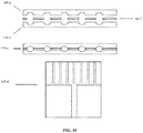
- dam and fill applications such as in RF-ID, one could apply a dam, cure it, and then fill and cure the fill. (See Fig. 9 ) However, one could co-cure the 2 adhesive beads using the method described in the current invention by the ability to couple more initiation energy into the containment bead as compared with the filler.
- the same base adhesive can be used for both cases (possibly the same chemical formulation) with the containment bead having a phosphor of a different conversion efficiency than that of the filler material. This can be readily done by proper choice of the phosphor, or content of the phosphor. In a way the adhesive beads can be cured effectively at the same time but one sees more UV intensity than the other and cure faster than the other under the same X-ray beam.
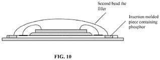
- an insertion molded piece of plastic containing the appropriate amount of phosphor is added as part of the material to be cured.
- this acts as the source of UV under X-ray energy.
- the inserted molded piece gives extra UV energy to the dam (or perimeter area) and leads to faster curing. This allows the materials to cure more selectively at the borders.
- This example describes the usefulness of insertion molding as described in Figure 10 .
- photo-sensitizing chemistries can be used to enhance the photo-catalytic based reactions.
- Synthesizing phosphors in the micron and nanometer particle sizes can be done using various methods. Also various phosphors may have different surface chemistries. Some phosphors could be potentially hygroscopic or toxic in high doses. One way to enable the use of hygroscopic or potentially toxic phosphors is to form a containing barrier layer around phosphor particles. This has the double benefit of standardizing different phosphor chemistries to have the same common surface chemistry with predictable behavior as well as shield the phosphor inside a barrier layer. A sol-gel derived silicate coating is one method by which this can be achieved. Silica happens to be UV transparent and is congruent with most oxides and most phosphors that are not hygroscopic (as listed in the phosphor table).
- the protective coating can be silica or can be diamond or diamond-like carbon.
- Silica can be formed using sol-gel derived techniques.
- Diamond and diamond-like carbon can be derived from CVD based on hydrogen-methane gas mixtures. These are but representative examples of the methods that are possible.
- the uniformity of dispersion of phosphors inside a resin is quite important.
- a uniform distribution of phosphors inside a curable system influences the homogeneity of the curable material and therefore the mechanical and optical properties of the curable material.
- the mixing uniformity and the particles size distribution have an influence on the curing system response in terms of cure extent as a function of time under the initiation energy.
- the uniformity of the dispersion can be short lived if the phosphors have a high specific density leading to settling in the resin. For this reason some surface modification techniques can be desirable to maintain the phosphors in suspension.
- the surface of the phosphors can be modified for 2 general purposes.
- One method leads to tethering or adsorbing the photo-initiators onto the surface of the phosphors.
- the other method is to add dispersant chemistries to the surface of phosphors to enable the phosphors to remain in suspension after the adhesive is formulated and the ingredients have been mixed together.
- phosphors are preferred to be in powder form with minimal aggregation between particles.
- the dispersion of phosphor powder in a resin system can be achieved using various methods. These dispersion methods keep the phosphors in suspension by limiting or preventing the potential re-flocculation caused by the particles' Brownian motion at room temperature or at temperatures above room temperatures by 20°C to 30°C. These slightly elevated above room temperature are useful in dispensing the adhesives through a needle using a piston or an auger pump.
- the surface modification of the phosphors to maintain a uniform dispersion after mixing is important.
- Various organic polymer agents can be used to increase the wetting characteristics of the phosphors into the resin chemistry.
- various dispersing agents can be added to maintain the phosphor particles in suspension inside the mix.
- the dispersing agents are built from polyurethane or polyacrylate polymeric structures having high molecular weight (3000-50000).
- Various dispersing agent are available in the market.
- the dispersants can be anchored onto inorganic surface by virtue of surface charge (the electrostatic attraction of oppositely charged surfaces) and can be anchored or adsorbed to the organic substances like the chains in the resin by virtue of dipolar interactions, hydrogen bonding and London/van-der-Waals forces. Once anchored in place the high molecular weight dispersants increase the steric hindrance for particles to diffuse too close to one another hence preventing agglomeration of phosphors.
- the downconverting particles and photo-initiators used in the present invention can be added as separate components to the curable adhesive formulation, or can be tethered to one another to provide increased likelihood of activation of the photoinitiator upon emission from the downconverting particles. Tethering of photoinitiators to the downconverting particles can be done by any conventional chemistry, so long as it does not interfere with the emission characterstics of the downconverting particles (other than potential slight movement of the peak emission in the red or blue direction), and so long as it does not interfere with the ability of the photoinitiator to initiate polymerization of the curable adhesive composition.
- organic downconverters such as anthracene
- organic downconverters there are additional possibilities including, but not limited to, use of the organic downconverter material as a separate component in the curable adhesive composition, tethering the organic downconverter to the photoinitiator, as described for the inorganic downconverter particles above, or even incorporation of the organic downconverter groups into one or more of the monomer components of the curable adhesive composition.
- the surface area (and hence the overall surface energy) of the nano-sized particles is very high, the viscosity rises quickly with the addition of a small amount of nano size powders. This limits the amount of filler that can be added. On one hand this limits the UV intensity that can be emitted by the phosphors under X-ray energy. On the other hand the limited filler loading that can be achieved is not economically favorable since fillers are typically less expensive than the base resins and catalysts. Furthermore, the viscosity increase with the addition of nano-size particles becomes excessive which limits the use of the adhesive to certain application categories but not others. In most adhesive application it is favorable to use micron size particles when possible. Though as stated earlier, the best mode calls for a bimodal particle size distribution consisting of mixture of nano and micron size particles.
- SiO 2 is more cost effective compared to phosphors. This is not always the case.
- One method by which enough UV light output is achieved while safeguarding a favorable economic phosphors-utilization is to build a composite particle based on SiO 2 as the core particle and decorated with the appropriate phosphors in terms of type and concentration necessary to achieve the targeted photo-catalytic reactions (i.e.; the right wavelength output and luminosity or intensity output).
- the surface of a carrier particle made of silica can be decorated with desirable phosphors with nanometer particle size.
- the phosphors are chosen for the right emission UV wavelength and intensity under X-ray.
- the downconverting particle comprises a composite of nanoparticles and a silicate carrier particle.
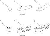
- the silicate carrier particle has the same surface characteristics as a particle typically used as a filler (including silica). In this case the down converting particles are bonded to the surface of the base carrier particle followed by a coating as shown in Figs. 11A and 11B .
- the core or carrier particle can be made of glass, such as SiO 2 or alkali-lead-silicate and have a diameter of about 2 microns.
- Nanometer-scale downconverting particles are applied to the surface of the core particle, and subsequently made to adhere or bond to the surface of the core particle (see Fig. 11B ). Some of the methods enabling this bonding process include precipitation techniques from a solution. Another method is based on condensation by heating the downconverting particles to much elevated temperatures compared to the core particles while maintaining the silicate based particles above their softening point.
- the downconverting particles and the carrier particles are forced into contact, leading to condensation, thus allowing surface deposition to take place.
- the downconverting particles can be any of the phosphors listed in the table.
- the downconverting particles can be quantum dots with the suitable range of downconversion from X-ray to UV.
- the quantum dots and/or oxides used for the downconversion process can further comprise elements, or alloys of compounds or elements tuned for plasmonic activity (see Fig. 12 ).
- the quantum dots preferably comprise a mixture of zinc sulfide and zinc selenide, more preferably in a ratio within a compositional window of 60% zinc sulfide, 40% zinc selenide to 70% zinc sulfide, 30% zinc selenide.
- the metal alloys used for plasmonics comprise silver/gold mixtures, more preferably within the compositional window of 60% silver and 40% gold, to 70% silver and 30% gold.
- the outer layer is desirable to encapsulate and protect the down converting particles as well as modify the surface.
- the outer layer coating can be accomplished using sol-gel processing followed by heat treatment. This leads to the formation of a composited particle consisting of a core particle with down-converting particles on the surface and the whole is coated with a silicate coating. (see Fig. 13 ). This special filler particle is used to replace an existing filler material.
- the present invention includes special provisions for a modified use of existing photoinitiators by tethering the photoinitiator to nanoparticles having downconverting properties. This close proximity of nanoparticle to photoinitiator maximizes the chance for photoinitiation or photo-catalysis, and can achieve improved cure efficiencies. (see Fig. 14 )
- the downconverting particles are added during mixing an adhesive preparation using tethered particles on a carrier particle and mixing into the adhesive.
- the tethered photoinitiator and downconverting particles can be positioned on the surfaces of micron level carrier particles. (See Figs. 15A and 15B )
- the carrier particles are then used as filler. This time no surface coating is necessary and the photoinitiator is in direct contact with the resin. ( Fig. 15A ).
- this arrangement can also use a coating of SiO 2 , on which are tethered the photoinitiators. ( Fig. 15B ).
- micron size particles large particles
- the impact on adhesive rheology is minimized compared to adding nano-size particles.
- This method can thus present added advantages, including the ability to use the micron size particles as a filler to otherwise alter the cured adhesive or polymer properties.
- Achieving brighter particles can be done by having the carrier particle decorated with 2 layers of phosphors. First the carrier particle is decorated with nano-sized phosphors ( Fig. 16A ), then coated using sol gel derived silica and lastly decorated a second time with phosphors of the correct size ( Fig. 16B ). This technique can be repeated to obtain more phosphors or down conversion particles at the outer-layers of the carrier particles.
- Adhesion develops through various factors including mechanical interlocking, adsorption, electrostatic, diffusion, weak boundary layer, acid base, chemical (covalent bonding), etc.
- mechanical interlocking adsorption, electrostatic, diffusion, weak boundary layer, acid base, chemical (covalent bonding), etc.
- the greater the surface irregularities and porosity at a joint area the greater the joint strength.
- joint strength The factors affecting joint strength include: surface energetics (wetting), intrinsic stresses and stress concentrations, mechanical response of various bulk phases and inter-phases involved, geometrical considerations, mode of applying external stresses, mode of fracture or separation, visco-elastic behavior.
- the wetting and the setting of the adhesive bead is important for a good bond formation.
- the spreading co-efficient of an adhesive depends on the various surfaces and associated surface tensions involved. The surface tensions are referred to here as the energetic requirements.
- the substrate (solid), the adhesive (liquid) and the vapor (open air in most cases) all play a role.
- Wetting of the surface depends on the surface energy between the solid and the liquid, the liquid to vapor surface tension and between solid to vapor surface tension.
- Substrates such as Teflon, PET, Nylon, PE, and PS have low energy.
- Substrates such as metals, metal oxides, and ceramics have high energy.
- the adhesive chemistry (the liquid in this example) can be tailored to adjust the energetic requirements at the various surfaces. But that is not sufficient. For example, most RTV silicone resins fulfill the energetic requirements but give negligible adhesion unless primers are used. Adhesive joints can be made stronger by surface treatments of the surfaces to be joined. Also inter-phases can be made between the adherend and the adhesive.
- Dry surface modification includes, but is not limited to, a surface plasma ionized through RF or microwave, flame, UV, UV sensitized, ozone, UV/ozone, X-ray, LASER, electron beam, ion bombardment, and friction against other materials.
- wet surface modification encompasses chemical reactions such as oxidation, sulfonation, ozonation, phosphatization, chromate conversion, amination, grafting, selective etching, deposition of coupling layers (silanes), surfactant adsorption, photochemical compounds, solvent (surface swelling), prevention of diffusion of low molecular weight materials to the surface, and others.
- One preferred embodiment involves the bonding of a silicon integrated circuit, either to a substrate or to another integrated circuit (to make a multilayer stack).
- the penetrating power of X-rays will be such that the X-rays can pass through the uppermost layer of silicon and reach the bond layer, in which the downconverting particles will become stimulated and emit the desired wavelength of light (which may be UV or visible, depending on the particular photoinitiator being used).
- Optional steps may include, without limitation: dispensing the adhesive in a pattern that will allow the adhesive to flow under a component through capillary action (e.g., "die underfill” processes); photo-patterning the adhesive; and applying pressure to the adhesive bond before and/or during the curing process.
- capillary action e.g., "die underfill” processes
- Optional components may include various organic or inorganic materials and additives to perform desired functions, such as modifying the electrical conductivity and dielectric properties of the cured polymer. Many of these components are well known to those skilled in the art.
- Conductive fillers may include finely divided particles of metals including gold, silver, nickel, copper, and alloys such as Au-Pd, Ag-Pd, etc.
- Other conductive phases that may be used with the invention include LaB 6 as well as various conductive oxides and carbon.
- the conductive filler particles may alternatively be made from small polymer beads or spheres having a conductive coating thereon, such as a thin gold film.
- the polymer particles may be fairly rigid or they may have some degree of flexibility or compressibility in order to make the final bond more compliant.
- Isotropic conductivity may be achieved by using small particles ("small” meaning particles with an average diameter much less than the final bond or film thickness) loaded to a volume fraction that exceeds the percolation threshold so that the resulting polymer composite material exhibits substantial electrical conductivity in every direction.
- the invention may also be used for anisotropic conductive materials, in which a film or sheet contains a monolayer of large individual spherical conductor particles ("large” meaning particles whose diameter is comparable to the final bond or film thickness) loaded to a volume fraction below the percolation threshold so that the resulting material is substantially conductive through the film thickness but is not conductive parallel to the plane of the film.
- suitable filler materials include various dielectric materials such as metal titanates and zirconates, titanium oxide, etc., that may be added to tailor the dielectric properties of the film.
- suitable inorganic additives may include boron nitride for applications where it is desired to have a bond that is electrically insulating yet thermally conductive.
- Organic additives may include several classes of agents familiar in the art. These include, without limitation: plasticizers to modify the mechanical properties of the cured polymer; surfactants and dispersants to modify the rheology of the uncured material to make it easier to dispense as well as to allow any particulate fillers to be adequately dispersed; and solvents and comonomers.
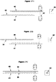
- an anisotropic conductive polymer sphere is generally represented at 10 of Fig. 17 .
- the sphere consists of an elastic polymer core 20 that is surrounded with a thin layer of plated nickel 22 under plated gold 24 and an outer layer of another, more brittle, thin polymer coating 36.
- Anisotropic Conductive Adhesives can be manufactured from rapid (snap-cure) thermo-setting epoxy resins filled with approximately 4% of conductive polymer spheres which have a nominal diameter of 5-microns.
- the polymer spheres are designed to deform elastically when compressed, exposing the outer gold plated surface, which is then able to establish electrical continuity across the narrow gap between aligned contact pads of stacked IC chips, wafers or other substrates.
- the polymer sphere 20' When compressed and deformed the polymer sphere 20' becomes partially flattened, as generally illustrated at 10' of Fig. 18 .
- the brittle outer polymer coating becomes fractured 36' at the top and bottom contact surfaces and exposes the malleable and partially flattened gold plating 24'.
- the gold plating still adheres to the partially flattened polymer sphere 20' by means of the plated nickel layer 22', which is also malleable and becomes partially flattened.
- the plated gold metal becomes exposed under compression it establishes a metal-to-metal electrical contact with the metal pads disposed directly above and below the partially flattened polymer sphere. Electrical continuity is then achieved across the gap between top and bottom pads around the circumference of each polymer sphere thru the plated nickel and gold layers. This process is further described and illustrated in Fig. 19 .
- the first essential step of the inventive method is to place a polymerizable adhesive composition, including a photoinitiator and downconverting phosphor, in contact with two or more components to be bonded to form an assembly.
- a polymerizable adhesive composition including a photoinitiator and downconverting phosphor
- the viscosity of the adhesive may be varied over a significant range by the choice of monomer(s), the possible use of solvents, the loading of filler particles, etc., as is well understood by skilled artisans.
- compositions will be thixotropic, enabling them to be conveniently dispensed using standard processes familiar in the field of adhesives.
- the compositions may be applied to selected areas using automated needle-type applicators in conjunction with pick-and-place methods. Alternatively, they may be applied in various patterns using printing through screens or masks. Low-viscosity systems, which would typically contain solvents and a minimal amount of inorganic fillers, may be distributed in selected patterns by ink-jet printing.
- the inventive material may be formed into a sheet having conductive balls of the appropriate diameter, cut or diced to a desired size, and placed between the two components to be bonded. It will be understood that in some cases, this process may be repeated in order to make a multilayer stack of any desired number of components.
- the second essential step of the inventive method is to irradiate the assembly with radiation at a first wavelength, capable of downconversion by the downconverter to a second wavelength capable of activating the photoinitiator, thus initiating the polymerization of the adhesive.
- the radiation applied to the assembly after the bond material has been placed will be X-rays.
- X-rays Many industrial X-ray generators are available commercially from a number of suppliers, and the skilled artisan may easily select an appropriate X-ray source based upon routine engineering considerations.
- thermo-set epoxy With the surfaces held in compression, using an externally applied force, the thermo-set epoxy is rapidly cured in order to maintain the conductive polymer spheres in a state of compression after the external force is removed.
- a thermo-set epoxy may be rapidly cured by means of an appropriate heat source such as a cartridge heater, microwave or ultrasonic generator, IR heat lamp, laser beam, or various other means to apply heat to the surfaces being bonded.
- the heat must generally be fairly high (>250°C) in order to achieve rapid curing of the epoxy and often requires that the heat be conducted through the surfaces used for achieving the applied force as well as the chip and/or substrate being bonded together.
- the epoxy can be cured without the necessity for using high heat. For example, if the epoxy can be cured at room temperature the materials may be joined without any residual shear stress thereby improving reliability. And if the fixtures used for aligning the parts and applying a compressive force between surfaces remain at room temperature, the time required for assembly may be substantially reduced.
- UV curable or visible light curable adhesive for manufacturing the ACA adhesives described above.
- Some literature has been written on this subject, but a fundamental problem arises when attempting to expose the adhesive to sufficient (curing) UV or light energy through optically opaque surfaces that are commonly encountered in microelectronic assembly. Without adequate UV or visible light illumination the epoxy may not fully polymerize. Some manufacturers attempt to remedy this situation by combining properties within the epoxy that allow it to be partially cured with UV-energy followed by a final thermal cure. However, an ideal UV or light-curable epoxy for ACA applications would be realized if it can be fully cured without necessity of an external UV or visible light source or additional thermal-cure steps.
- various photoinitiator compounds and downconverting materials exist that can convert absorbed higher-energy (X-ray) photons to lower-energy photons (UV or visible light).
- an adhesive epoxy is custom engineered to be sensitive (i.e. polymerize) when exposed to the spectral wavelength and energy level of one or more types of these "down-converting" lower-energy photon emitters, included as a "filler" within the epoxy, then the epoxy can be fully cured, even through optically opaque materials, by exposing it to an X-ray source.
- An added benefit is that the same X-ray energy may simultaneously be detected and converted into an image for quality control purposes.
- Fig. 19 An example of an X-ray activated, UV or visible light curable, anisotropic conductive adhesive (ACA) ( 35 ) is shown in Fig. 19 .
- IC integrated chip
- the bumps ( 32 ) on the bottom surface of the flip chip device are raised above the otherwise planar surface of the IC chip.
- the raised bumps are typically fashioned using either electro-plated or electro-less plating methods and may consist of metals such as nickel-gold, copper-nickel-gold, titanium-tungsten/copper/nickel/gold and other various metals and/or alloy combinations.
- the raised bumps typically range in height from 5-10 microns above the planar surface of the IC.
- the raised bumps are typically formed on the chips while they are still part of the whole wafer.
- the substrate will typically not include raised bumps.
- the raised bumps on the IC form a difference in thickness of the gap between the surfaces.
- ACA polymer spheres approximately 4% of 5 micron diameter spheres
- the "proper" amount of force required is determined experimentally depending on the variable geometries and materials that are being assembled.
- the remaining AC polymer spheres ( 10 ) that fall between adjacent bumps will remain un-compressed and will not generally conduct electricity, since the brittle polymer coating (36) is unbroken.
- the X-ray activated adhesive (35) is also filled with small down-converting photon emitters (38) which are engineered to emit lower-energy photons in the UV or visible light spectrum.
- the amount and size of these down-converting photon emitters would also be experimentally determined, depending on the material properties. In practice, the down-converting photon emitter particles would be smaller than the AC polymer spheres ( 10 or 10' ) and would be evenly distributed within the epoxy resin (35).
- the down-converting photon emitters may adversely effect the viscosity and thixotropic characteristics of the UV adhesive. Therefore, an alternative and better practice would be to substitute the polymer coating (36) of the ACA polymer spheres (10) with a coating (26) consisting of the down-converting photon emitter material(s), to form a new type of anisotropic conductive, UV emitting, polymer sphere ( 11 ) as illustrated in Fig. 20 .
- the down-converting photon emitter coating is both electrically nonconductive and brittle in nature, so as to fracture when partially flattened (26') and thereby expose the gold coating (24') underneath, as illustrated in Fig. 21 .
- Fig. 22 is similar to Fig. 19 , but illustrates the absence of the down-converting photon emitter "filler” particles (38) and substitution of anisotropic conductive, UV emitting, polymer spheres ( 11 and 11' ), as previously described. These polymer spheres would be similar in size and volume to existing ACA adhesive formulations and therefore would be expected to perform in a similar manner.
- FIG. 23 Another example of an assembly using anisotropic conductive, UV emitting, polymer spheres ( 11 and 11' ) is shown in Fig. 23 .
- This illustration shows two similar IC wafers, such as memory chip wafers, stacked one above the other and electrically and mechanically joined together.
- Both the top IC wafer (40) and bottom IC wafer (41) include "Through Silicon Via” (TSV) contacts (42) that provide a means for routing circuit interconnections from the top (active) surface of the wafer to pads arrayed across the bottom surface of the wafer.
- TSV Thinitride
- TSV contacts include small, raised, annular or square pads on the top and bottom surfaces that form contact surfaces for electrical connection through the partially flattened polymer spheres ( 11' ).
- An X-ray wafer aligner and bonder (39) of Fig. 24A is designed to enable wafer-to-wafer alignment and bonding using an X-ray activated, UV or visible light curable, ACA epoxy (35) without need for applying external heat to the wafer surfaces being joined.
- the bonder includes two vacuum plates (44), of sufficient size to hold a top IC wafer (40) and bottom IC-wafer (41), that are spaced apart sufficient to enable a split field prism and lens device (46) to be temporarily inserted and scanned between the surfaces, as shown.
- the prism device is used to precisely align the wafer surfaces with respect to one another, either manually or by automated means, prior to the wafer surfaces being compressed together.
- the prism device provides a means to view and superimpose fiducial images from multiple locations on the bottom surface of the upper wafer with similar fiducial images on a top view of the lower wafer.
- the split field prism and lens device are removed and the wafers are brought together under an applied force (48) as shown in Fig. 24B .
- the applied force compresses and partially flattens the anisotropic conductive polymer spheres (10' or 11') trapped between the aligned flip chip device bumps (32) and/or Thru Silicon Via (TSV) contacts (42) of each IC on the two wafers, as previously described and shown in Figures 19 , 22 and 23 .
- an X-ray Exposure Device (50) and X-ray imaging device (52) are brought into position, as shown in Fig. 24C .
- X-ray exposure device (50) is used to generate a field of high energy photons that stimulate the fluorescent coating of the down-converting spheres which then spontaneously emit UV light of the correct wavelength and luminosity to cause the UV resin to rapidly cure by photo initiation.
- the high energy photons may also advantageously be detected on the surface of an X-ray imaging detector (52), positioned directly across from the X-ray exposure device and on the opposite side of the wafer vacuum plates.
- the X-ray imaging detector is designed to produce high resolution X-ray images of the bonded surfaces using analog and/or digital circuitry that is immune to damage from the X-ray source.
- Data from the X-ray imaging detector is collected and processed into high-resolution digital images, as either individual photos and/or continuous video, for data (archival) storage and/or image processing to provide a means for process and quality control.
- FIGs. 25A-C An alternative technique to achieve wafer-to-wafer alignment is illustrated in Figs. 25A-C .
- the movable split field prism and lens devices (46) are replaced by a pair of fixed lens (47) that remain stationary as the wafers are individually moved over or under the field of view of the lens-pair to locate alignment fiducials (49 and 49') disposed at multiple locations near the edges of both top and bottom IC-wafers.
- Alignment fiducials for the top IC-wafer (49) differ from the bottom IC-wafer (49') and are designed to be superimposed over each other to provide an optical reference for precise alignment in the x-axis, y-axis and theta-angle.
- the fiducial images (49 and 49') as shown in Figs. 25A and 25B would be superimposed, as illustrated at 51 of Fig. 25C .
- top and/or bottom IC-wafers Disposed on the top and/or bottom IC-wafers (40 and 41) are coatings of a UV-curable, ACA filled epoxy (35) and/or compatible matrix epoxy resin (34).
- a UV-curable, ACA filled epoxy 35) and/or compatible matrix epoxy resin (34).
- the bottom epoxy coating may include ACA conductive spheres (10 or 11) within a high-viscosity resin matrix
- the top IC-wafer may be coated with a compatible resin that has a lower viscosity and does not contain any ACA conductive spheres.
- the differing compositions and viscosities of the coatings allow for a reduction in the amount of ACA spheres required to achieve reliable interconnect between stacked chips or wafers, enables better retention of individual ACA spheres where required on the bumped pads during application of the compressive force during bonding, and helps to reduce formation of voids within the cured epoxy.
- the surfaces are brought together and compressed under an applied force to enable the ACA polymer spheres to deform and establish electrical continuity between juxtaposed pads of the individuals IC devices on the wafers; thereby establishing a 3-D interconnect between surfaces.
- the pads that are to be joined may not have identical coefficient of thermal expansion (CTE) values, the polymer spheres provide a compliant interface that helps to absorb expansion mismatch during thermal cycling, thereby maintaining proper electrical continuity.
- CTE coefficient of thermal expansion
- the resin and the photo-initiator materials were obtained from BASF.
- the materials were weighted in the proper ratios using a balance having +/ 0.1 grams measurement accuracy.
- the materials were mixed in a laboratory environment with DCA (a class 10,000 clean room). All materials handling was done in a fume-hood. The laboratory had a fluorescent light source to light the room while the fume hood had a controlled light (no UV component to it).
- the substrates used to demonstrate bonding included glass, polycarbonates, poly ethylene terephthalate, poly-imides, cellulose (or paper), cross-ply carbon-prepreg composites, PEC, ABS, Mylar, intrinsic silicon, doped silicon, silicon based integrated circuits.
- the materials were mixed in the proper ratios then they were transferred to syringes and subsequently centrifuged to remove air-bubbles. In other cases, the materials were placed in syringes but not centrifuged. Yet in another case the materials were enclosed inside of the mixing cups. Depending on the specific density of the materials, a high level or a low level of sedimentation was observed.
- the materials preparation further included the addition of dispersants in an attempt to control sedimentation. In these cases the surface of the phosphors was modified to enable the attachment of dispersants.
- the materials were then mixed inside resin materials and photo-initiators under heat. The materials were hand mixed using a stainless steel spatula that did not react or contaminate the raw materials. No materials contaminations were at play for the most part.
- the temperature used for mixing varied from room temperature to 80°C. The mixing was better when conducted at elevated temperatures.
- the sequence of mixing was investigated. Various mixing sequences may work. However, a preferred embodiment of preparation is obtained by heating the resin materials to 80°C followed by adding the photo-initiators and mixing. The mixing and heating of the resin and photo-initiators is continued until a clear (air bubble free) solution is obtained. Mixing is done gently to avoid shearing the resins and the photo-initiators. Heating was found to have a significant impact in this step.
- the phosphors are added third followed by mixing. In this case the mixing is continued until the phosphors are well dispersed inside the solution before adding a filler material. Phosphor materials having particle size distributions in the micron scale are best. The filler materials are added last.
- the filler material is Y 2 O 3 :Gd nanoparticles and a fractional amount of Aerosil (or active silica). Filler materials in the nanoscale particle size worked best. It is of interest to note that in this case the Y 2 O 3 :Gd consists of 5 to 60 nm particles and that the Aerosil material has fibrous like morphology. It is also of interest to note that the Y 2 O 3 :Gd particles can agglomerate and could form micron level aggregates. The resolution as what these aggregates could help is not clear.
- the original intent was to determine the proper UV response and the adhesion between substrates at room temperature and with no other UV light source except from the conversion of X-ray into UV.
- the mixing of raw materials was performed with the fluorescent room light on. It was discovered that the elapsed time under room fluorescent light influenced the outcome of the cure extent. In essence, the UV light from the room assisted in photo-initiating the chemical reaction. The longer the elapsed time for mixing under uncontrolled light, the more cure extent was achieved under X-ray energy.
- a controlled photo-catalysis initiation was performed to take advantage of this discovery. This was called flashing the material with a UV light prior to curing under X-ray.
- the initiation of the photo-catalytic reactions in adhesive materials was achieved through UV-flashing by the following sequence in the preparation.
- the raw materials were prepared under controlled light only.
- the photo-catalysis initiation was performed using a set time exposure to UV light soon after the dispensing/application of the adhesive or during the dispensing/application of the adhesive prior to the placement of the top substrate.
- the sandwiched part was then placed under X-ray energy and cured farther.
- the materials that were subjected to flashing cured faster than those that were not subjected to flashing. Based on cure hardness the flashing of select chemistries was done in less than (7.5 min) while the same select chemistries took longer (12.5 minutes) when no flashing was applied.
- the flashing is further exemplified in the following Figs. 26A-C .
- a hand held or automatic piston pump dispenser 70 was used in this case.
- the adhesive bead 60 was dispensed on substrate element 72 illustrated in Fig. 26A .
- the substrate in this case was polycarbonate.
- the dispenser applied the bead using a needle gauge 22. No phosphor segregation was observable using a piston pump of the appropriate gauge.
- Fig. 26B the bottom substrate 72 had a spacer element 74 made of Kapton and having a thickness of 90 microns.
- a UV source 73 was used to apply energy from within UVA range centered around 365nm see Fig. 27 . After 15 seconds to 25 seconds of UVA exposure another substrate element 72" was applied on top. The assembly hence formed was taken to the X-ray system for curing. It is recognized that the UV flashing can be done for longer times as needed; however, there a practical limitation to UV flashing.
- the UV flashing is an effective method that allows the reaction to be boosted from a cost effective source. Subsequently to the flashing and almost immediately, the substrates to be joined need to be placed against one another. The adhesive bead is then placed inside an X-ray system. The X-ray energy can effectively complete the reaction of an adhesive bead that is inside a no line of sight region of an assembly.
- the ability to dispense and flash the adhesive can be done with a high degree of repeatability using an automatic dispenser having a mechanical drive consisting of a servo motor or a cable drive.
- the robotic system is equipped with mechanical coupling mechanisms (or articulations) 78 and a mechanical arm 77 to enable the placement of the adhesive dispense needle in a precise manner over a large area.
- the mechanical system further comprises a drive system 76 based on a servo motor or simply a cable drive.
- the system can further comprise a platen 79 that is equipped with vacuum ports 79' and a source of heat 79" such as a thermode (refer to Fig. 29 ).
- a source of heat 79" such as a thermode (refer to Fig. 29 ).
- the vacuum helps secure the substrates in place.
- the thermode increases temperature of the substrate. Adhesives at slightly elevated temperature can flow much more readily than at room temperature.
- the viscosity of adhesives is typically lowered at elevated temperatures until curing starts taking place in which case the viscosity starts increasing. their viscosity, this is beneficial in specific applications but not others. Some applications require the wicking of adhesives through capillary forces underneath substrates or into porous materials.
- the adhesion is promoted by having elevating the temperature.
- the upper most temperature to which the substrate can be heated should be below its glass transition temperature (Tg). Below Tg the substrate expands at one coefficient of thermal expansion and above its Tg the substrate's at a higher coefficient of thermal expansion. As long as the temperature remains below Tg the adhesion could be promoted.
- the UV flashing is accompanied by the curing of the outer layer (or the formation of a skin).
- This outer layer or skin reaches higher cure extent than the inside portion of the bead.
- the bead becomes unpractical because of the hardened outer layer becomes an impediment to the controlled placement of the top substrate.
- the formation of an adhesive bond line through the juxtaposition of 2 substrates becomes hard to do.
- the steps described above were repeated without any UV flashing. So that the adhesive bead was prepared under controlled light inside the fume-hood and kept shielded from light exposure until we exposed to the adhesive bead to X-ray energy. In this case the adhesive curing was conducted for 12.5 minutes to reach adequate mechanical bonding.
- a screen printer can be used instead of an adhesive dispenser.
- the substrate element 72 is positioned under the screen 90.
- a screen aperture 90' can be positioned above the substrate 72 but not contacting it.
- a blade 91 is passed with an adequate pressure to force the adhesive through the screen aperture.
- the screen is subsequently removed.
- the dispensed adhesive 60' is exposed to UV energy for a controlled time (between 15 and 25 seconds).
- the top substrate is then positioned on top of the adhesive.
- the sandwiched bead can be cured in X-ray for 7.5 min and successfully bond the 2 substrates.
- the substrate was cross-ply carbon composite 80 in Fig. 31A-C .
- the adhesive 60 was applied to the adhesive.
- a component made of PET 81 was placed on the uncured adhesive bead.
- the assembly hence formed was turned around and placed under an X-ray source for curing. No flashing was used in this case.
- the adhesive bead cured in 15 minutes.
- the X-ray curing system can have an additional source of radiation, namely UV.
- the UV radiation from the UV source 73 can be used in conjunction with the X-ray radiation from X-ray source 82. This enables the cure of adhesive beads that have a portion that is exposed to the outside world and a portion that has no line of sight. An example is described in Fig. 32 where a fillet 60" has direct line of sight and can be cured using radiation.
- the fillet 60" plays in an important role in flip chip applications where stresses are maximal at the corner of the IC chips.
- the curing of the fillet 60" can be done using an adequate recipe to minimize stresses. This would imply that the curing using UV radiation can be done simultaneously, before or after the X_Ray radiation whichever minimizes the inherent stresses.
- a dispenser 70 contains adhesive 60 while dispenser 70" contains adhesive 61.
- the 2 beads are dispensed sequentially.
- a novel adhesive applicator is conceived.
- the novel dispenser 64 has 2 chambers and 2 coaxial needles as illustrated in Fig. 33A-C .
- the inside container 62 contains adhesive 61 while the external container 63 contains adhesive 63.
- the novel dispenser has a coaxial needle containing needle 64' and 64" through which adhesives 61 and 60 flow respectively.
- the adhesives were applied to the substrates using various methods from simple to more complex.
- the adhesive formulations were scooped from the mixing cup using a spatula and deposited on the top surface of one substrate.
- the adhesives were placed in syringes and hand pressed through a needle with an 18 to 22 gauge.
- the materials were dispensed through the needle of EDF air piston pump (also using 18 to 22 gauge needles).
- the substrates had a spacer element sandwiched between the substrates to keep the materials from being squeezed out from between the substrates.
- the adhesive cure was demonstrated for adhesive bead thicknesses from 60 microns to 1000 microns.
- the spacer elements were glass beads.
- the curing of the adhesive thickness of the adhesive beads was successfully demonstrated at 60 microns to 250 microns. These thicknesses represent adhesive beads that would be compatible with applications such as B-staged films and chip on board applications. In other cases the adhesive bead was between 500 microns to 1000 microns. These thicknesses represent adhesive beads that would be compatible with applications such as hermetic sealing applications.
- the control over the rheology and thickness of the adhesive beads was achieved using filler elements such as AEROSIL and nanoparticles of doped Y 2 O 3 . Gadolinium was found to be the preferred doping elements in these cases. In order to achieve thicknesses of 500 microns and above the adhesive formulations had between 0.5% and 5% of filler.
- the adhesive bead was applied between 2 polycarbonate substrates and kept in this configuration for 24 hours. No-flow or displacement was observable.
- the adhesive bead was therefore made to provide the end -user with enough work and pot life after dispense and to tolerate interruptions of the work in process during manufacturing. This is significant because no scarping of the work in process after dispense is required.
- Formulations 1 2 3 4 5 6 Resin 5 5 5 5 - - Resin (shadow cure) - - - - 5 5 PI (369) 1.3 1.3 1.3 1.3 1.3 - - PI (2959) - - - - 0.5 0.5 LaOB:Tm 1.5 2.5 3.5 2.5 2.5 2.5 Y 2 O 3 - - - 0.3 - - AEROSIL 0.2 0.2 0.2 0.2 0.2 0.2 0.2 CABOSIL - - - - - MEKP - - - 0 0.1 -
- recipe number 2 3 and 4 cured faster than other formulations.
- adhesion was compromised when excess photo-initiator was used. For this reason recipe 4 worked best. It cured faster that recipe 2 and had better adhesion than recipe 3.
- the first substrate is positioned in place. The location of the substrate and the mechanical registration is recorded.
- the adhesive is then applied to the first substrate.
- the adhesive may contain a contrast agent to resolute a bead pattern on top of the first substrate.
- a first substrate that is black should not have an adhesive color that is black.
- a white or off-white colored bead would be more suitable.
- a whitening agent like TiO 2 can be used as the contrasting agent. In this case the color of the substrate is irrelevant, since the inspection can be performed using X-ray radiation, the inspection of the bead can simply be done regardless of the visible color contrast.
- the second substrate is then positioned in place on top of the adhesive bead and the first substrate.
- the assembly is transported under the X-ray system that would perform a combination of X-ray based steps namely inspection and cure or one step consisting of curing.
- the X-ray system comprises various elements that can be automated to satisfy manufacturing requirements.
- Fig. 34 illustrates some of these elements that form the X-ray curing system intended by the invention.
- the step of X-ray radiation is preferably done in an enclosure 83 that stops the radiation from leaking to the outside world.
- the enclosure 83 can be made of various materials that include heavy metals such as lead.
- a single assembly 72' can be held static or can be moved during cure inside the enclosure. Such movement could include a rotation movement that can be achieved using a turn table. Such movement could also include a translational movement that can be achieved using an external conveyor belt 85 and an internal conveyor 85'. Both the internal and the external conveyor belts work in synch to shuttle parts in and out of the X-ray enclosure.
- the door 84 can open up and close down to shuttle assemblies 72' in and out of the X-ray radiation chamber. When the door is open (or up position) the X-ray energy is off to adhere to safety measures.
- the X-ray enclosure can have automated doors with sensors linked to a controller 76'.
- the enclosure can have doors that open up and down to shuttle at least one assembly in and out of the X-ray enclosure for irradiation leading to curing.
- the assembly to be cured can be positioned inside a process fixture 86.
- the process fixture carries with it the assemblies 72'.
- More than one assembly can be placed inside the X-ray machine.
- the configuration having multiple assemblies can vary to maximize the loading of parts inside the X-ray curing system.
- 2 conveyors are juxtaposed one next to the other to increase the packing factor (number of assemblies) inside the X-ray system within plane. Because of the depth of penetration at the correct levels, conveyors can be disposed within planes ( Fig. 35A ) and across planes ( Fig. 35B ) inside the X-ray curing system.
- An additional advantage of X-ray curing resides in its ability to cure various size adhesive beads residing within different products using the same curing parameters.
- the X-ray machine can have more than one source, permitting curing of different assemblies at the same time (see Fig. 36 ). This presents an advantage and enables the manufacturer to cure different product mix inside the X-ray curing system. Assemblies 160 and 160' can be cured at the same time. This means that a product change over is easier and that the system is flexible in meeting cure requirements.
- X-ray systems with the capability of programming recipes including pulsing up to 30 times per sec can be done.
- a level of control over the kvp as well as amperage can be done to exert control over output power as well as photon energy which in turns means control over depth of penetration.
- curing time and efficiency can be adjusted as desired by adjustment of various parameters, including, but not limited to, temperature, radiation source intensity, distance of the radiation source from the adhesive composition to be cured, and photon flux generated by the radiation source.
- X-ray delivery head is on one side of the assembly, either above the adhesive bead or below the adhesive bead which can be described (though not exact) that the adhesive bead is generally perpendicular to the direction of propagation. In some cases the adhesive bead is generally parallel to the X-ray radiation path. It is recognized however that the X-ray radiation is emitted in a flood beam have multiple directions around one predominant direction of propagation.
- Figs. 37A-C Two configurations are possible. In one case Fig. 37A . the assemblies are oriented vertically to achieve the preferred orientation, in the other case Fig. 37B , the X-ray source(s) is mounted in the appropriated orientation to achieve the desirable alignment between bead and direction of propagation. Fig. 37C provides a different view of the alignment between assembly 160 and the X-ray.
- the wafers are clamped together using a clamping fixture 88.
- the clamping fixture allows the wafers to remain aligned during transport.
- the clamping fixture contacts the wafers on the wafer back side with a depth typically within the exclusion zone of the wafers.
- the wafers can be placed on a rotating table 89 with a rotating arm 87 as illustrated in Fig. 38A and Fig. 38B .
- the rotating table is capable of taking withstanding pressure up to 40 kN.
- the pressure can be applied using 2 mirror image rotating tables.
- the clamping fixture 88 can be removed once the 2 rotating table have been engaged.
- the die on wafer application could use the same wafer set up described in Fig. 39 .
- the X-ray is aligned at an angle which leads to more depth of penetration over the area array of the ICs 40' disposed on top of the bottom wafer 41.
- the plane of the bond line in this case is at 45 degrees vis-à-vis the direction of propagation of the X-ray.
- Containers that can be raised up and down to gate the assemblies 160 that enters the processing chamber.
- Part of the cavity 90' can be raised to enable batching of assemblies 160.
- Chamber 120 is fixed in place.
- the bottom of the cavity of chamber 122 can be raised up and down to enable positioning wafers 41 that enter the processing station.
- the movable bottom does not touch the upper processing chamber (no contact between 120 and 122.
- a composite panel 80 is dispensed with adhesive 60.
- the metallic fastener 110 is placed on top of the substrate 80 using a pick and place system that is pneumatically driven (112). Both the pick and place 112 and the adhesive dispenser 111 are mounted on KUKA robot 113.
- the X-ray sources 82 are placed at a slight angle to couple to the bottom of the bolt 110.
- the following figures show various applications in semiconductors pertaining to packaging and encapsulation. These include: glob top, dam and fill, molding (PMC, insertion molding) and flip chip underfill.
- An IC 28 is soldered in place in such manner that bumps 32 enter into electrical contacts with electrical pads 132.
- a desirable adhesive 60-1 is applied by dispensing system 70 (see Fig. 44 ). If the substrate is heated to 20°C above room temperature the adhesive wicks under the chip by virtue of the capillary forces set between the chip and the substrate 72 . Once the adhesive is dispensed and wicked under the IC, the adhesive is ready for curing and optionally an inspection is performed prior to curing. The standard method is to inspect the adhesive using optical means. However, since the adhesive 60-1 is loaded with phosphors that have absorption characteristics in the X-ray regime, the inspection can be performed using X-ray radiation. The inspection using X-ray can reveal any striations that may exist under the IC 28. The uniformity of the adhesive can be determined to see if the adhesive has separated into resin rich or resin poor regions. The adhesive can be subsequently cured with X-ray.
- the curing in this case can be done at room temperature and the X-ray is best coupled from the lateral side of the IC. In this case the direction of propagation is parallel to the plane of the adhesive bead.
- Fig. 45 illustrates the various elements.
- an encapsulant (60-2) can be dispensed on top of a substrate (72') above the area array of contact pads (132). See Fig. 46 .
- An optical inspection is performed. A chip is picked using a programmable "Pick & Place” (130) having provisions for vacuum (131). An active alignment is performed before the chip is placed onto a PCB (72') in such manner that the IC bumps (32) enter into electrical contacts with PCB electrical pads (132).
- the no-flow adhesive can be inspected and cured using X-ray.
- the glob top applications comprise dispensing an electronic polymer on top of an IC (28) that has been die attached onto a PCB (72') and wire bonded to establish electrical contacts between the active area of IC (28) and the electrical pads (132) disposed on the PCB board (72') See Fig. 47 .
- the special adhesive (60-3) containing the appropriate phosphors and photo-initiators can be applied to the IC (28) and enough time is allowed for the electronic polymer to flow and to cover the IC (28) and wire bonds (132').
- the assembly is then inspected using X-ray radiation and cured using an X-ray radiation treatment or recipe.
- the X-ray treatment can consist of pulses of controllable duration appropriate to harden the adhesive without inducing any damage to the assembly.
- a dam 60-4) or the first adhesive bead and subsequently cure the first bead prior to dispensing an encapsulant (60-1) containing the appropriate phosphors and photo-initiators required for X-ray curing.
- the current technology allows co-curing of both 60-1 and 60-4 using X-ray radiation. See Fig. 48 .
- the amount of phosphors loaded in formulation 60-4 can be deliberately high to cure faster than 60-1.
- Another standardized way of applying the encapsulation is through injection molding.
- the resin is applied at the mold level.
- the IC (28) is attached to the substrate (72") and then inserted into a mold.
- the mold is then clamped at high pressure and a liquid resin at high temperature is injected at high pressures to fill the spaces between the wire bonds (132') and the IC (28) See Fig. 49 .
- the injection molding step is then accompanied by an elongated heat treatment.
- the present invention is enabled through the use of a low-viscosity resin (60-5) that contains the appropriate phosphors and photo-initiators. After the injection molding at low temperature is performed, the X-ray inspection and X-ray curing can take place.
- the benefits of using the present invention are various but the most pronounced benefit to release all the stresses that can be established post molding. This eliminates most thermal annealing steps required for stress release. These stress release steps can take up to 4 hours which increases the Work-In-Process and does not lead to favorable economics.
- lid sealing See Figs.50A and 50B .
- three different adhesives can be used.
- the combination of 3 different adhesives can be used: 1-An adhesive bead (60), 2- an underfill adhesive (60-1), and 3- thermal conductive adhesive (60-6) that connects IC 28 with a lid 133.
- the lid 133 is typically metallic.
- the lid 133' could be glass.
- a micro-ball-grid-array can be encapsulated in much the same way that was described for the glob top encapsulation.
- the configuration of the assembly is different than a chip on board application but the encapsulation of the wire bonds 132' remains the same. (see Fig. 51 )
- An appropriate encapsulation 60-3 with the proper viscosity is prepared to contain the amount of photo-initiators and phosphors to cure under X-ray.
- TAB Tape automatic bonding
- plastic 140-a to plastic parts 140-b that has mirror image features can be used to build functional plastic containers that house fluids and that have usable fluidic channels that can channel fluids from one side of the container to the other.
- the 2 pieces of plastics having mate-able features are joined together using a film adhesive 60-7 to form piece 140c.(illustrating a cross sectional view).
- the film 60-7 has the proper resin and the proper phosphors and photo-initiators.
- the plastic housing formed is illustrated as part 140d (top view). See Fig. 53 .
- the fluidic channels can be formed using multiple pieces of plastics.
- the cross section of a PET plastic is shown in 150.
- the PET has well joints as shown by groves 100.
- the fluidic channels 102' are aligned with the fluidic channels 102 present on another plastic such as Liquid Crystal Polymer 150'
- the sub-assemblies hence formed can be used to form fluidic devices.
- An example of such sub-assemblies is provided.
- Each part of the subassembly can have conduits and interlocking features to allow apertures to be aligned.
- the adhesive bead 60-3 is dispensed and allowed to cure using X-ray. See Figs. 54A and 54B .
- the subassemblies are collapsed controllably.
- the protruding features 101 enter into the well joint 100. These features enable the obtainment of a hermetic seal since a fluid (liquid of gas) has to travel through the split well that is formed when the protruding feature 101 is engaged inside the well joint 100. The travel distance increases and the hermetic seal is enhanced.
- Yet another example includes when a flexible circuit 134 having contact pads 132.
- the flex 134 is TAB bonded to IC 150 using adhesive 60-3.
- the IC 150 has a resistive heating network that can increase the temperature around fluidic channels or apertures 102.
- the fluidic channels 102 are aligned with apertures or fluidic channels 102' that exist on plastic parts 145-d.
- the IC 150 is bonded using adhesive 60.
- the fluidic channels 102' connect with fluidic reservoirs 152. These reservoirs can contain Ink or insulin. See Figs. 55A and 55B .
- the adhesive film 60-7 is activated to bond the outer walls of 145d with the flex 134.
- the plastic joining does not have to use mirror image plastics nor does it have to use similar materials. In fact dissimilar materials can be used to form plastic housing for insulin pumps or inkjet containers.
- Ink jet cartridges are typically made of a plastic housing made of a thermoplastic moldable resin, such as polyethylene terephthalate (PET), polyethylene, or polysulfone for example, as the base material.
- a thermoplastic moldable resin such as polyethylene terephthalate (PET), polyethylene, or polysulfone for example, as the base material.
- PET polyethylene terephthalate
- Polysulfone describes a family of thermoplastic polymers that have toughness, mechanical stability and ink resistance.
- a print head made of silicon has numerous nozzles that are used as ink outlets.
- the nozzle array on the silicon and the ink reservoirs are connected through a manifold structure having fluidic channels.
- the fluidic channels are employed to direct the inks of different colors from the primary reservoirs to appropriate printhead nozzle arrays.
- Multicolor cartridges have a plurality of ink reservoirs, often three ink reservoirs. In such three ink cartridges, each of the reservoirs contains a primary color. These reservoirs need to be isolated from one another. The separation between the compartments has to be hermetic to avoid ink mixing between the various compartments. A plastic piece is adhesively bonded to seal the separate reservoirs.
- the joint of interest that seals or separates the various reservoirs must be made to withstand the prolonged contact with inks. Inks happen to be aggressive from a chemical stand point. Furthermore, the sealing joint needs to be able to overcome the mechanical stresses that may exist over the product's functional life and the pressure differential that needs to be regulated between atmospheric pressure and the internal pressure in the reservoir.
- the ink reservoirs and the ink channels, the plastic structures and manifolds necessary to form the multicolor cartridge can be assembled from multiple injection molded plastic parts.
- the most economical way is to injection mold as one part all of these parts.
- the lid seal and the tri-chamber separation cannot be injection molded as a unitary body, since it is required to have accessibility to the reservoirs.
- two process methods are typically used to bond plastics: Ultrasonic energy welding and thermally curable adhesives.
- the problem with ultrasonic welding is that it does not work with dissimilar materials.
- the other method consists of using adhesive materials to bond the various parts together.
- the various plastics parts in this case can be of similar or dissimilar materials provided the adhesive is subjected to enough thermal energy.
- the print head is connected to a flexible circuit using a TAB bonding method.
- the print head rests on an adhesive bead that bonds the print head to the manifold containing fluidic channels.
- the print head contains nozzles that can be fired by the electrical signal that feed a resistive network built on the silicon.
- the electrical signals that are selectively applied to specific nozzles results in the heating of the select nozzles and therefore leads to the controllable ejection or squirting of ink droplets.
- the ink droplets are directed to the print media like paper to form patterns leading to words, images and the like.
- the present invention adhesive composition can be used in the formation of inkjet cartridges, such as those described above or in formation of inkjet cartridges according to the conventional art, such as US Patent 7,832,839 ; US Patent 7,547,098 ; or US 7,815,300 , for example, the contents of each of which are hereby incorporated by reference.
- Fiber element 91 can be straight or can be flexible to adopt various shapes.
- the fiber element leaks UV energy around its core and along the direction of propagation of the UV light. When light is coupled from its ends the light propagate along the fiber and leaks UV lights to its environment. (see Figs. 56A and 56B )
- the fiber element is inserted in a joint between 2 plastics.
- An adhesive is dispensed around the fiber and the assemblies are collapsed together.
- the curing can therefore be achieved by coupling UV to the external sides of the fiber element to distribute UV light to the inside of the assembly. (See Figs. 57A and 57B )
- the CaWO 4 phosphors and CaWO 4 :Pb emits in the visible and UVA under x-ray energy. Both these phosphors have a notoriously slow decay time. This phosphor keeps on emitting visible and UV light even after the initiating energy has stopped. The emission remains strong for 60 to 100 seconds after x-ray energy irradiation has stopped.
- the CaWO 4 as well as the CaWO 4 :Pb can be applied for a delayed curing application such as UV inks.
- the UV ink offers the possibility of rapid cure under UV light.
- the inclusion of nano-particle size phosphors that have light modulating capability from x-ray and extreme UV to a desirable UVA and visible range are particularly preferred.
- the initiating radiation can flash (short burst exposure) the ink and the included phosphors with delay decay time can keep on emitting UV radiation that can cure the ink.
- These special inks can be used in digital presses equipped with EUV or x-ray sources to flash activate the phosphors with slow decay times.
- the web-speed can therefore be accelerated from 400 feet per minute to over 900 feet per minute by virtue of the sustainable UV emissions that can keep on curing the inks from within the thickness of the ink itself.
- the glossy paper offers limited porosity if any. For this reason, inks wetting the surface remain in wet form and do not dry quickly. Thermal energy can be imparted to the surface of the web to assist in removing the solvents used in the inks. The solvents have a slow drying rates and cannot be easily removed which slows down the web speed.
- thermal energy and an initiation radiation can be used in the present invention.
- a reel of glossy paper (200) feeds a portion of the digital printing press described in FIG. 58 .
- the paper is imparted with ink though an ink dispensing station (201).
- the source of an initiation radiation (202) flashes the ink with x-ray or EUV.
- the phosphors embedded within the ink and having a slow decay time are activated with the x-ray or EUV.
- the paper moves to the thermal station (203).
- the paper is then turned around a first pulley (204) and a second pulley (204).
- the back side of the paper is now ready for printing using a ink dispensing station (201).
- the thermal treatment as well as the UV flashing is imparted on the ink using station 203 and 202.
- the paper is then moved to another portion of the digital printing press.
- the present invention adhesives can also be used in the formation of composites, by the adhesion of two or more plies, which are the fundamental building blocks of layered composites.
- the composites can be built by layering the plies, with the plies adhered one to the other using the adhesive composition of the present invention.
- Any conventional ply can be prepared, such as -45+45 assemblies (See FIGS. 59A and B ), 0+90 composites (see FIGS. 60A and B ).
- the composite is preferably formed by preparation of a prepreg material formed of the plurality of plies, with each ply placed in the desired configuration with respect to the other plies, and having the curable adhesive composition of the present invention between respective layers of the plies.
- the curable adhesive can be cured by application of the desired ionizing radiation, such as X-rays, thereby adhering the plies together to form the composite.
- the adhesive composition of the present invention can alternatively be used in photolithography as a curable resin to accomplish either negative or positive photo-resist development.
- By the use of heavy metal masking elements it is possible to get selective curing of the present invention composition to form desired patterns or semiconductor elements.
- the adhesive composition can be doped with electroconductive fillers, as desired.
- the downconverting particles can be adhered to a thin film (preferably to both sides of the thin film) which can be placed between two surfaces, each of which is coated with the curable adhesive monomer and photoinitiator formulation. Upon irradiation, the downconverting particles emit energy at the desired wavelength, activating the photoinitiator, and initiating curing of both layers of adhesive, thus bonding each of the surfaces to an opposite side of the thin film having the downconverting particles.
- a thin film preferably to both sides of the thin film
- the downconverting particles Upon irradiation, the downconverting particles emit energy at the desired wavelength, activating the photoinitiator, and initiating curing of both layers of adhesive, thus bonding each of the surfaces to an opposite side of the thin film having the downconverting particles.
- the materials chemistries were prepared by first weighing the key chemical ingredients and mixing these chemical ingredients under heat.
- a functionalized Acrylate resin was obtained from BASF.
- the resin was made from a mixture of 4 commercially available products including Laromer LR 9023, Laromer PO 94F, Laromer TPGDA, Laromer LR 9004.
- the photoinitiators were also obtained from BASF and consisted of IRGACURE 369 and IRGACURE 2529.
- the phosphors were obtained from Phosphor Technologies.
- the LaOBr:Tb 3+ phosphor as well as the YTaO 4 were used in the preparation of the curing formulations.
- the third phosphor was Y 2 O 3 doped with Gadolinium (Y 2 O 3 :Gd). This third phosphor was synthesized in nano-particle size. It was used both as a phosphor and as a thickening agent.
- the temperature that was used during all the mixing steps was 80°C.
- the sequence of adding the various chemicals was as follows: 1- resin, 2- photoinitiator, 3- phosphor and 4-thickening agent.
- the thickening agent was the Y 2 O 3 :Gd. The mixtures stirred every 10 minutes for one hour to two hours. This ensured the obtainment of a homogenous mixture.
- MEKP was added to an adhesive formulation to assess the effectiveness of X-Ray curing on coupling energy to MEKP and enhancing the cure kinetics. It was found that recipe or formulation number 2, 3 and 4 cured faster than other formulations. However adhesion was compromised when excess photo-initiator was used. For this reason recipe 4worked best. It cured faster that recipe 2 and had better adhesion than recipe 3.
- Curing of the various formulations was done on PET, glass, polycarbonate, polyimide, polysulfone, a carbon prepreg, a FR4 PCB.
- the adhesive bead was sandwiched between two similar substrates and cured while in between the substrates. No temperature was increased while in the x-ray. The temperature was measured using a hand-held IR thermometer. The only time a noticeable temperature increase of up to 10°C was observed is in the case of the formulation containing MEKP.
- Additional formulations were cured.
- the elapsed time under X-Ray was 10 min, 12.5 min, 15 min, 17.5 min and 20 min.
- the formulations that were made using the LaOBr:Tb 3+ phosphor cured between 10 min and 12.5 min.
- the formulations that were made using the phosphor YTaO 4 cured between 12.5 min and 15 min.
- the formulations using the third phosphor was Y 2 O 3 doped with Gadolinium (Y 2 O 3 :Gd) cured in 17.5 minutes.
- the LaOBr:Tb 3+ mixed with Y 2 O 3 :Gd were added to the adhesive formulations, the cure was accomplished in 10 min.
Landscapes
- Chemical & Material Sciences (AREA)
- Organic Chemistry (AREA)
- Engineering & Computer Science (AREA)
- Health & Medical Sciences (AREA)
- Materials Engineering (AREA)
- Inorganic Chemistry (AREA)
- Life Sciences & Earth Sciences (AREA)
- Surgery (AREA)
- Chemical Kinetics & Catalysis (AREA)
- Animal Behavior & Ethology (AREA)
- Manufacturing & Machinery (AREA)
- Veterinary Medicine (AREA)
- Public Health (AREA)
- General Health & Medical Sciences (AREA)
- Medicinal Chemistry (AREA)
- Polymers & Plastics (AREA)
- Thermal Sciences (AREA)
- Plasma & Fusion (AREA)
- Physics & Mathematics (AREA)
- Nuclear Medicine, Radiotherapy & Molecular Imaging (AREA)
- Molecular Biology (AREA)
- Medical Informatics (AREA)
- Heart & Thoracic Surgery (AREA)
- Epidemiology (AREA)
- Ceramic Engineering (AREA)
- Biomedical Technology (AREA)
- Cardiology (AREA)
- Adhesives Or Adhesive Processes (AREA)
Claims (19)
- Härtbare Klebstoffzusammensetzung, umfassend:ein organisches Vehikel, umfassend mindestens ein polymerisierbares Monomer, das beim Aushärten ein Harz bildet;mindestens ein Photoinitiator, der auf eine ausgewählte Lichtwellenlänge anspricht; undmindestens ein Energieumwandlungsmaterial, das ausgewählt ist, um die Lichtwellenlänge zu emittieren, wenn es einer ausgewählten übermittelten Strahlung ausgesetzt wird;wobei das organische Vehikel der Teil der härtbaren Klebstoffzusammensetzung ist, der letztendlich das Harz durch die Polymerisation bildet, undwobei das Energieumwandlungsmaterial imstande ist, eine übermittelte Energie zu absorbieren und die Energie umzuwandeln, um Photonen in einem Spektralbereich zu erzeugen, der von dem mindestens einen Photoinitiator absorbiert werden kann, und somit die Polymerisation des mindestens einen polymerisierbaren Monomers zu initiieren.
- Härtbare Klebstoffzusammensetzung nach Anspruch 1, wobei das mindestens eine Energieumwandlungsmaterial ein hochkonvertierendes (upconverting) Material ist.
- Härtbare Klebstoffzusammensetzung nach Anspruch 1, wobei das mindestens eine Energieumwandlungsmaterial ein herabkonvertierendes (downconverting) Material ist.
- Härtbare Klebstoffzusammensetzung nach Anspruch 1 oder 3, wobei die übermittelte Strahlung eine ionisierende Strahlung ist.
- Härtbare Klebstoffzusammensetzung nach einem der Ansprüche 1 bis 4, wobei das organische Vehikel ein Monomer umfasst, das ein duroplastisches Harz bildet.
- Härtbare Klebstoffzusammensetzung nach Anspruch 5, wobei das duroplastische Harz ausgewählt ist aus der Gruppe bestehend aus: Acrylen, Phenolen, Urethanen, Epoxiden, Styrolen und Silikonen.
- Härtbare Klebstoffzusammensetzung nach einem der Ansprüche 1 bis 6, wobei der mindestens eine Photoinitiator ausgewählt ist aus der Gruppe bestehend aus: Benzoinethern, Benzilketalen, α-Dialkoxyacetophenonen, α-Aminoalkylphenonen, Acylphosphinoxiden, Benzophenonen/Aminen, Thioxanthonen/Amine und Titanocenen.
- Härtbare Klebstoffzusammensetzung nach Anspruch 4, wobei die Lichtwellenlänge im UV-Bereich liegt und die ionisierende Strahlung Röntgenstrahlen umfasst.
- Härtbare Klebstoffzusammensetzung nach Anspruch 3, wobei das herabkonvertierende Material dispergierte anorganische Partikel umfasst, die ausgewählt sind aus der Gruppe bestehend aus: Metalloxiden; Metallsulfiden; dotierten Metalloxiden; und gemischten Metallchalkogeniden.
- Härtbare Klebstoffzusammensetzung nach einem der Ansprüche 1 bis 9, wobei der Klebstoff fotomusterfähig ist.
- Härtbare Klebstoffzusammensetzung nach einem der Ansprüche 1 bis 10, ferner umfassend:- anorganische Partikel, ausgewählt aus der Gruppe bestehend aus: Metallen und Metalllegierungen, Keramiken und Dielektrika sowie metallbeschichteten Polymeren;- eine organische Komponente, die ausgewählt ist aus der Gruppe bestehend aus: Lösungsmitteln, Viskositätsmodifikatoren, Tensiden, Dispergiermitteln und Weichmachern.
- Verfahren zum Kleben, umfassend:a) Platzieren einer härtbaren Klebstoffzusammensetzung nach einem der Ansprüche 1 bis 11 in Kontakt mit mindestens zwei zu verbindenden Komponenten, um eine Anordnung zu bilden, wobei die mindestens zwei Komponenten aus demselben Material oder aus verschiedenen Materialien gebildet sein können; und,b) Bestrahlen der Anordnung mit Strahlung einer ersten Wellenlänge, die durch das mindestens eine Energieumwandlungsmaterial in eine zweite Wellenlänge umgewandelt werden kann, die den mindestens einen Photoinitiator aktivieren kann, wodurch der mindestens eine Photoinitiator aktiviert wird und die härtbare Klebstoffzusammensetzung härtet, um die mindestens zwei Komponenten miteinander zu verbinden.
- Tintenstrahlpatrone, umfassend einen Druckkopf und einen Kartuschenkörper, wobei der Druckkopf und der Kartuschenkörper durch eine gehärtete Klebstoffzusammensetzung zusammengehalten werden, die durch Härten einer härtbaren Klebstoffzusammensetzung gemäß einem der Ansprüche 1 bis 11 gebildet wurde.
- Wafer-zu-Wafer-Verbundanordnung, umfassend mehrere Halbleiterwafer, die durch eine gehärtete Klebstoffzusammensetzung miteinander verbunden sind, die durch Härten einer härtbaren Klebstoffzusammensetzung nach einem der Ansprüche 1 bis 11 erhalten wurde.
- Baugruppe mit integrierter Schaltung, umfassend mehrere elektrisch verbundene Materialschichten, wobei die mehreren elektrisch verbundenen Materialschichten durch eine gehärtete Klebstoffzusammensetzung zusammengehalten werden, die durch Härten einer härtbaren Klebstoffzusammensetzung gemäß einem der Ansprüche 1 bis 11 erhalten wurde, und wobei die integrierte Schaltung keine externen leitenden Verbindungen zwischen den Schichten aufweist.
- Folie, die zwischen zwei zu verbindenden Komponenten angeordnet ist und leitende Kugeln einer geeigneten Größe aufweist, um die resultierende Klebeverbindung anisotrop leitend zu machen, wobei die Folie aus der härtbaren Klebstoffzusammensetzung nach einem der Ansprüche 1 bis 11 gebildet wird.
- Verfahren zum Verbinden von ungleichen Substraten miteinander, umfassend:Bereitstellen eines ersten Substrats und eines zweiten Substrats, wobei das erste Substrat ein anderes Material als das zweite Substrat umfasst;Aufbringen einer härtbaren Klebstoffzusammensetzung nach einem der Ansprüche 1 bis 11 auf eine Oberfläche von mindestens dem ersten Substrat;Inkontaktbringen der Oberfläche des ersten Substrats, das die härtbare Klebstoffzusammensetzung trägt, mit einer Oberfläche des zweiten Substrats; undHärten der härtbaren Klebstoffzusammensetzung durch Anwenden der übermittelten Strahlung.
- Verfahren zum Kleben von lebendem Gewebe, umfassend:a) Aufbringen einer härtbaren Klebstoffzusammensetzung nach einem der Ansprüche 1 bis 11 in Kontakt mit mindestens zwei Teilen des zu klebenden lebenden Gewebes; und,b) Bestrahlen der Anordnung mit Strahlung einer ersten Wellenlänge, die durch das mindestens eine Energieumwandlungsmaterial in eine zweite Wellenlänge umgewandelt werden kann, die den mindestens einen Photoinitiator aktivieren kann, wodurch der mindestens eine Photoinitiator aktiviert wird und die härtbare Klebstoffzusammensetzung härtet um die mindestens zwei Teile des lebenden Gewebes miteinander zu verbinden.
- Ausgehärteter Klebstoff, der aus der härtbaren Klebstoffzusammensetzung nach einem der Ansprüche 1 bis 11 gebildet ist.
Priority Applications (3)
| Application Number | Priority Date | Filing Date | Title |
|---|---|---|---|
| HRP20210997TT HRP20210997T1 (hr) | 2010-05-06 | 2011-05-06 | Pripravak za spajanje lijepljenjem i način uporabe |
| SI201131981T SI2567257T1 (sl) | 2010-05-06 | 2011-05-06 | Lepilni vezivni sestavek in postopek uporabe |
| EP21152905.2A EP3839572B1 (de) | 2010-05-06 | 2011-05-06 | Haftbindungszusammensetzung und verfahren zu ihrer verwendung |
Applications Claiming Priority (3)
| Application Number | Priority Date | Filing Date | Title |
|---|---|---|---|
| US33199010P | 2010-05-06 | 2010-05-06 | |
| US201161443019P | 2011-02-15 | 2011-02-15 | |
| PCT/US2011/035565 WO2011140469A1 (en) | 2010-05-06 | 2011-05-06 | Adhesive bonding composition and method of use |
Related Child Applications (2)
| Application Number | Title | Priority Date | Filing Date |
|---|---|---|---|
| EP21152905.2A Division EP3839572B1 (de) | 2010-05-06 | 2011-05-06 | Haftbindungszusammensetzung und verfahren zu ihrer verwendung |
| EP21152905.2A Division-Into EP3839572B1 (de) | 2010-05-06 | 2011-05-06 | Haftbindungszusammensetzung und verfahren zu ihrer verwendung |
Publications (3)
| Publication Number | Publication Date |
|---|---|
| EP2567257A1 EP2567257A1 (de) | 2013-03-13 |
| EP2567257A4 EP2567257A4 (de) | 2015-07-08 |
| EP2567257B1 true EP2567257B1 (de) | 2021-03-24 |
Family
ID=44904107
Family Applications (2)
| Application Number | Title | Priority Date | Filing Date |
|---|---|---|---|
| EP11778432.2A Active EP2567257B1 (de) | 2010-05-06 | 2011-05-06 | Haftbindungszusammensetzung und verfahren zu ihrer verwendung |
| EP21152905.2A Active EP3839572B1 (de) | 2010-05-06 | 2011-05-06 | Haftbindungszusammensetzung und verfahren zu ihrer verwendung |
Family Applications After (1)
| Application Number | Title | Priority Date | Filing Date |
|---|---|---|---|
| EP21152905.2A Active EP3839572B1 (de) | 2010-05-06 | 2011-05-06 | Haftbindungszusammensetzung und verfahren zu ihrer verwendung |
Country Status (7)
| Country | Link |
|---|---|
| US (7) | US9023249B2 (de) |
| EP (2) | EP2567257B1 (de) |
| ES (1) | ES2880840T3 (de) |
| HR (1) | HRP20210997T1 (de) |
| PT (1) | PT2567257T (de) |
| SI (1) | SI2567257T1 (de) |
| WO (1) | WO2011140469A1 (de) |
Families Citing this family (104)
| Publication number | Priority date | Publication date | Assignee | Title |
|---|---|---|---|---|
| US9488916B2 (en) | 2007-04-08 | 2016-11-08 | Immunolight, Llc. | Interior energy-activation of photo-reactive species inside a medium or body |
| US10087343B2 (en) * | 2007-08-06 | 2018-10-02 | Immunolight, Llc | Adhesive bonding composition and method of use |
| US9676918B2 (en) | 2007-08-06 | 2017-06-13 | Immunolight, Llc. | On demand radiation induced constructive and deconstructive chemical reactions |
| US10410991B2 (en) | 2007-08-06 | 2019-09-10 | Immunolight, Llc | Adhesive bonding composition and method of use |
| US8899171B2 (en) | 2008-06-13 | 2014-12-02 | Kateeva, Inc. | Gas enclosure assembly and system |
| US9048344B2 (en) | 2008-06-13 | 2015-06-02 | Kateeva, Inc. | Gas enclosure assembly and system |
| US10434804B2 (en) | 2008-06-13 | 2019-10-08 | Kateeva, Inc. | Low particle gas enclosure systems and methods |
| US11975546B2 (en) | 2008-06-13 | 2024-05-07 | Kateeva, Inc. | Gas enclosure assembly and system |
| US12018857B2 (en) | 2008-06-13 | 2024-06-25 | Kateeva, Inc. | Gas enclosure assembly and system |
| US12064979B2 (en) | 2008-06-13 | 2024-08-20 | Kateeva, Inc. | Low-particle gas enclosure systems and methods |
| US9604245B2 (en) | 2008-06-13 | 2017-03-28 | Kateeva, Inc. | Gas enclosure systems and methods utilizing an auxiliary enclosure |
| US8383202B2 (en) | 2008-06-13 | 2013-02-26 | Kateeva, Inc. | Method and apparatus for load-locked printing |
| EP2567257B1 (de) | 2010-05-06 | 2021-03-24 | Immunolight, Llc. | Haftbindungszusammensetzung und verfahren zu ihrer verwendung |
| US9120344B2 (en) | 2011-08-09 | 2015-09-01 | Kateeva, Inc. | Apparatus and method for control of print gap |
| KR102016871B1 (ko) | 2011-08-09 | 2019-08-30 | 카티바, 인크. | 하향 인쇄 장치 및 방법 |
| CN103176365A (zh) * | 2011-12-22 | 2013-06-26 | 深圳富泰宏精密工业有限公司 | 菲林及其制作方法,应用该菲林进行遮蔽的方法 |
| US20130206630A1 (en) | 2012-02-14 | 2013-08-15 | SteriPax, Inc. | Design control water based adhesive |
| US10012288B2 (en) * | 2012-03-16 | 2018-07-03 | Charles Steahly | Glue-on attachable flywheel weight |
| TWI448538B (zh) | 2012-10-23 | 2014-08-11 | Ind Tech Res Inst | 螢光材料與紫外光發光裝置 |
| DE202013012393U1 (de) * | 2012-10-26 | 2016-09-05 | Zhuhai Ninestar Management Co., Ltd. | Steuereinheit zur Lichtsteuerung einer Tintenpatrone, Platine und Tintenpatrone |
| KR101965127B1 (ko) | 2012-10-29 | 2019-04-04 | 삼성전자 주식회사 | 반도체 패키지 및 그 제조 방법 |
| CN104797192B (zh) * | 2012-11-21 | 2018-02-06 | 柯尼卡美能达株式会社 | 便携型放射线图像摄影装置 |
| DE102012221942A1 (de) * | 2012-11-30 | 2014-06-05 | Wobben Properties Gmbh | Verfahren zur Bearbeltung eines Faserkunststoffverbundes eines Rotorblattes, Halbzeug in Form eines Aufbauverbundes und UV-Lampe zum Aushärten eines UV-aushärtbaren Matrixmaterials |
| US20140166202A1 (en) * | 2012-12-11 | 2014-06-19 | Immunolight, Llc. | Bonding of substrates induced by ionizing radiation |
| US9431274B2 (en) * | 2012-12-20 | 2016-08-30 | Intel Corporation | Method for reducing underfill filler settling in integrated circuit packages |
| US9243784B2 (en) | 2012-12-20 | 2016-01-26 | International Business Machines Corporation | Semiconductor photonic package |
| CN103111408B (zh) * | 2013-02-04 | 2014-07-09 | 北京六同志远科技有限公司 | 用于点胶的紫外光源随动固化装置及使用其的点胶机 |
| US9400356B2 (en) | 2013-03-14 | 2016-07-26 | International Business Machines Corporation | Fiber pigtail with integrated lid |
| US8923665B2 (en) | 2013-03-15 | 2014-12-30 | International Business Machines Corporation | Material structures for front-end of the line integration of optical polarization splitters and rotators |
| WO2014168578A1 (en) * | 2013-04-10 | 2014-10-16 | Applied Materials South East Asia Pte. Ltd. | Wafer bonding total thickness variation improvement by contour confinement method |
| JP6318025B2 (ja) * | 2013-06-27 | 2018-04-25 | 積水化学工業株式会社 | 導電性粒子、導電材料及び接続構造体 |
| US10174223B2 (en) * | 2013-11-30 | 2019-01-08 | Hrl Laboratories, Llc | Formulations, methods, and apparatus for remote triggering of frontally cured polymers |
| US9269596B2 (en) * | 2013-12-19 | 2016-02-23 | Intel Corporation | Narrow-gap flip chip underfill composition |
| CN105900258A (zh) | 2013-12-26 | 2016-08-24 | 科迪华公司 | 电子装置的热加工 |
| WO2015099781A1 (en) * | 2013-12-27 | 2015-07-02 | xyINTEL CORPORATION | Optoelectronic packaging assemblies |
| KR102050152B1 (ko) | 2014-01-21 | 2020-01-08 | 카티바, 인크. | 전자 장치 인캡슐레이션을 위한 기기 및 기술 |
| US9343678B2 (en) | 2014-01-21 | 2016-05-17 | Kateeva, Inc. | Apparatus and techniques for electronic device encapsulation |
| JP6331525B2 (ja) * | 2014-03-14 | 2018-05-30 | オムロン株式会社 | 樹脂組成物の硬化方法 |
| ES2948676T3 (es) * | 2014-03-18 | 2023-09-15 | Immunolight Llc | Composición de unión adhesiva mejorada y método de uso |
| US9565773B2 (en) | 2014-03-31 | 2017-02-07 | Apple Inc. | Methods for assembling electronic devices with adhesive |
| KR102390045B1 (ko) * | 2014-04-30 | 2022-04-22 | 카티바, 인크. | 가스 쿠션 장비 및 기판 코팅 기술 |
| EP2960306B1 (de) * | 2014-06-26 | 2020-12-23 | Agfa Nv | Wässrige strahlungshärtbare Tintenstrahltinten |
| US9929124B2 (en) | 2014-06-26 | 2018-03-27 | Ev Group E. Thallner Gmbh | Method for bonding substrates |
| EP3160734B1 (de) | 2014-06-30 | 2023-09-06 | Immunolight, Llc. | Verbesserte haftbindungszusammensetzung und verfahren zur verwendung |
| US9285542B2 (en) | 2014-07-09 | 2016-03-15 | International Business Machines Corporation | Fiber optic interface with adhesive fill system |
| US20160046843A1 (en) * | 2014-08-13 | 2016-02-18 | R.R. Donnelley & Sons Company | Adhesive composition for inkjet printing |
| US9714367B1 (en) * | 2014-10-03 | 2017-07-25 | Verily Life Sciences Llc | Light curable adhesives |
| CN107111212B (zh) * | 2014-11-12 | 2019-11-12 | 艾斯科技公司 | 摄像头模块自动对焦致动器及其控制方法 |
| US10428176B2 (en) * | 2014-12-09 | 2019-10-01 | Korea Institute Of Industrial Technology | Thermosetting alkoxysilyl compound having two or more alkoxysilyl groups, composition and cured product comprising same, use thereof, and method for preparing alkoxysilyl compound |
| DE102014225396B3 (de) * | 2014-12-10 | 2016-04-28 | Siemens Aktiengesellschaft | Sensorboard für ein Detektormodul und Verfahren zu dessen Herstellung |
| PL3253341T3 (pl) | 2015-02-02 | 2019-06-28 | Coloplast A/S | Urządzenie stomijne |
| JP6243368B2 (ja) * | 2015-02-27 | 2017-12-06 | ファナック株式会社 | エネルギー線硬化型接着剤により部品を接着する接着方法 |
| DK3280368T3 (da) | 2015-04-10 | 2019-09-23 | Coloplast As | Stomianordning |
| CN104793408A (zh) * | 2015-05-07 | 2015-07-22 | 合肥鑫晟光电科技有限公司 | 显示面板及显示装置 |
| CN107849265A (zh) * | 2015-05-14 | 2018-03-27 | 加州理工学院 | 使用上转换纳米颗粒和近红外(nir)光的光可调人工晶状体 |
| ES2908622T3 (es) * | 2015-06-15 | 2022-05-03 | Immunolight Llc | Reacciones químicas constructivas y deconstructivas inducidas por radiación bajo demanda |
| NL1041407B1 (en) | 2015-07-24 | 2017-02-07 | Qmicro B V | Microfluidic device. |
| US10568726B2 (en) | 2015-08-06 | 2020-02-25 | Transparent Materials, Llc | Photocomposite, light source and thermal detector |
| US20170176116A1 (en) * | 2015-12-18 | 2017-06-22 | Renee Wu | Formable interface and shielding structures |
| DE102015016702A1 (de) * | 2015-12-22 | 2017-06-22 | Man Truck & Bus Ag | Partikelteilchen aufweisendes Klebemittel zur Verbindung zweier Fahrzeugteile |
| US10224219B2 (en) | 2015-12-30 | 2019-03-05 | International Business Machines Corporation | Handler bonding and debonding for semiconductor dies |
| US9947570B2 (en) | 2015-12-30 | 2018-04-17 | International Business Machines Corporation | Handler bonding and debonding for semiconductor dies |
| DE102015122950B4 (de) * | 2015-12-30 | 2024-06-06 | Fraunhofer-Gesellschaft zur Förderung der angewandten Forschung e.V. | Verbundanker |
| DE102016206088A1 (de) * | 2016-04-12 | 2017-05-24 | Carl Zeiss Smt Gmbh | Verfahren zum Bestimmen der Dicke einer kontaminierenden Schicht und/oder der Art eines kontaminierenden Materials, optisches Element und EUV-Lithographiesystem |
| CN106297959A (zh) * | 2016-11-01 | 2017-01-04 | 京东方科技集团股份有限公司 | 导电粒子、各向异性导电膜层及其制备方法和显示装置 |
| KR102711850B1 (ko) * | 2016-11-30 | 2024-10-02 | 엘지디스플레이 주식회사 | 이방성 도전필름 및 이를 포함하는 표시장치 |
| KR102555383B1 (ko) * | 2016-12-07 | 2023-07-12 | 엘지디스플레이 주식회사 | 유기발광소자를 이용한 조명장치 및 그 제조방법 |
| US9865527B1 (en) | 2016-12-22 | 2018-01-09 | Texas Instruments Incorporated | Packaged semiconductor device having nanoparticle adhesion layer patterned into zones of electrical conductance and insulation |
| MY195254A (en) * | 2017-01-11 | 2023-01-11 | Hitachi Chemical Co Ltd | Copper Paste for Pressureless Bonding, Bonded Body And Semiconductor Device |
| US9941194B1 (en) * | 2017-02-21 | 2018-04-10 | Texas Instruments Incorporated | Packaged semiconductor device having patterned conductance dual-material nanoparticle adhesion layer |
| US10283476B2 (en) * | 2017-03-15 | 2019-05-07 | Immunolight, Llc. | Adhesive bonding composition and electronic components prepared from the same |
| US10696899B2 (en) | 2017-05-09 | 2020-06-30 | International Business Machines Corporation | Light emitting shell in multi-compartment microcapsules |
| US10900908B2 (en) | 2017-05-24 | 2021-01-26 | International Business Machines Corporation | Chemiluminescence for tamper event detection |
| US10357921B2 (en) | 2017-05-24 | 2019-07-23 | International Business Machines Corporation | Light generating microcapsules for photo-curing |
| TWI618206B (zh) * | 2017-06-09 | 2018-03-11 | Phoenix Pioneer Technology Co., Ltd. | 半導體封裝結構及其製作方法 |
| US10392452B2 (en) | 2017-06-23 | 2019-08-27 | International Business Machines Corporation | Light generating microcapsules for self-healing polymer applications |
| US10765777B2 (en) * | 2017-06-28 | 2020-09-08 | California Institute Of Technology | Light adjustable intraocular lenses using upconverting core-shell nanoparticles and near infrared (NIR) light |
| JP7092474B2 (ja) * | 2017-08-21 | 2022-06-28 | シチズン電子株式会社 | 発光装置 |
| JP7077584B2 (ja) * | 2017-11-15 | 2022-05-31 | セイコーエプソン株式会社 | Memsデバイス、液体吐出ヘッド、および液体吐出装置 |
| KR102450580B1 (ko) | 2017-12-22 | 2022-10-07 | 삼성전자주식회사 | 금속 배선 하부의 절연층 구조를 갖는 반도체 장치 |
| US10770432B2 (en) | 2018-03-13 | 2020-09-08 | Stmicroelectronics S.R.L. | ASICS face to face self assembly |
| US10600937B1 (en) * | 2018-09-17 | 2020-03-24 | Lumileds Holding B.V. | Precise bondline control between LED components |
| CN108957899B (zh) * | 2018-09-25 | 2023-06-06 | 无锡威峰科技股份有限公司 | 一种双层微结构的显示电浆模组及其制造方法 |
| US10573544B1 (en) * | 2018-10-17 | 2020-02-25 | X-Celeprint Limited | Micro-transfer printing with selective component removal |
| US10796938B2 (en) | 2018-10-17 | 2020-10-06 | X Display Company Technology Limited | Micro-transfer printing with selective component removal |
| US11488841B2 (en) * | 2019-02-20 | 2022-11-01 | Electronics And Telecommunications Research Institute | Method for manufacturing semiconductor package |
| MA55220A (fr) | 2019-03-04 | 2022-01-12 | Immunolight Llc | Structures d'augmentation d'énergie destinées à être utilisées avec des émetteurs et des collecteurs d'énergie |
| US11424224B2 (en) * | 2019-04-24 | 2022-08-23 | Seoul Viosys Co., Ltd. | LED display panel, LED display apparatus having the same and method of fabricating the same |
| US11062976B2 (en) * | 2019-05-03 | 2021-07-13 | International Business Machines Corporation | Functional stiffener that enables land grid array interconnections and power decoupling |
| BR112022003051A2 (pt) * | 2019-09-13 | 2022-08-16 | Holistick Medical | Implante médico, dispositivo de entrega, método de produção de implante médico, e método de colocação de implante médico |
| WO2020082092A1 (en) * | 2019-10-23 | 2020-04-23 | Futurewei Technologies, Inc. | Precision chip bonding by adhesive wicking |
| KR102342827B1 (ko) * | 2019-11-18 | 2021-12-24 | 그린정보통신(주) | 반도체 포토리소그래피 공정의 웨이퍼 결함 검출 시스템 |
| CN110993519B (zh) * | 2019-11-21 | 2021-08-24 | 京东方科技集团股份有限公司 | 芯片绑定方法 |
| WO2021211129A1 (en) * | 2020-04-16 | 2021-10-21 | Hewlett-Packard Development Company, L.P. | Conductive connections |
| US11940340B2 (en) * | 2020-05-13 | 2024-03-26 | Hutchinson Technology Incorporated | Integrated sensors |
| CN111530703B (zh) * | 2020-06-05 | 2025-06-24 | 无锡嘉硕科技有限公司 | 一种石英晶体谐振器的特殊点胶针及点胶方法 |
| TWI755034B (zh) * | 2020-08-19 | 2022-02-11 | 友達光電股份有限公司 | 元件基板及其製造方法 |
| JP7381174B2 (ja) * | 2021-05-21 | 2023-11-15 | 三菱電機株式会社 | 光モジュール |
| US12362316B2 (en) * | 2022-02-11 | 2025-07-15 | Advanced Semiconductor Engineering, Inc. | Electronic structure having a protrusion structure disposed in a gap between a circuit pattern structure and a packaging structure |
| US12249561B2 (en) * | 2022-05-13 | 2025-03-11 | Infineon Technologies Ag | Semiconductor device arrangement with compressible adhesive |
| WO2025014812A2 (en) * | 2023-07-07 | 2025-01-16 | Supernal, Llc | Needling and welding systems, methods, and devices |
| US12362237B1 (en) * | 2024-04-05 | 2025-07-15 | Wolfspeed, Inc. | Fill-in planarization system and method |
| WO2025259673A1 (en) * | 2024-06-10 | 2025-12-18 | Immunolight, Llc | Color enhancing optical light propagators, optical films, color enhancing films, and film assemblies, articles containing the same, and methods for preparing the same |
| WO2026014351A1 (ja) * | 2024-07-12 | 2026-01-15 | ナミックス株式会社 | 光硬化性樹脂組成物、接着剤、封止材、コーティング剤、硬化物、半導体装置、電子部品、並びに光硬化性樹脂組成物を使用する硬化、接着、封止及びコーティング方法 |
Family Cites Families (29)
| Publication number | Priority date | Publication date | Assignee | Title |
|---|---|---|---|---|
| US3043708A (en) | 1958-07-22 | 1962-07-10 | Dunlop Rubber Co | Modified carbon black |
| US3555908A (en) | 1969-03-03 | 1971-01-19 | Honeywell Inc | Altitude indicator |
| US4256108A (en) | 1977-04-07 | 1981-03-17 | Alza Corporation | Microporous-semipermeable laminated osmotic system |
| US5198541A (en) | 1987-08-11 | 1993-03-30 | New York University | Dna encoding bactericidal/permeability-increasing proteins |
| US5395688A (en) * | 1987-10-26 | 1995-03-07 | Baxter Diagnostics Inc. | Magnetically responsive fluorescent polymer particles |
| US5537133A (en) * | 1992-04-02 | 1996-07-16 | Hewlett-Packard Company | Restraining element for a print cartridge body to reduce thermally induced stress |
| US5506608A (en) * | 1992-04-02 | 1996-04-09 | Hewlett-Packard Company | Print cartridge body and nozzle member having similar coefficient of thermal expansion |
| US5648806A (en) * | 1992-04-02 | 1997-07-15 | Hewlett-Packard Company | Stable substrate structure for a wide swath nozzle array in a high resolution inkjet printer |
| US5467115A (en) * | 1992-04-02 | 1995-11-14 | Hewlett-Packard Company | Inkjet printhead formed to eliminate ink trajectory errors |
| US5685074A (en) * | 1992-04-02 | 1997-11-11 | Hewlett-Packard Company | Method of forming an inkjet printhead with trench and backward peninsulas |
| US5450113A (en) * | 1992-04-02 | 1995-09-12 | Hewlett-Packard Company | Inkjet printhead with improved seal arrangement |
| US5755032A (en) * | 1992-04-02 | 1998-05-26 | Hewlett-Packard Company | Method of forming an inkjet printhead with channels connecting trench and firing chambers |
| US5519425A (en) * | 1993-11-15 | 1996-05-21 | Xerox Corporation | Ink supply cartridge for an ink jet printer |
| JPH1011822A (ja) * | 1996-06-26 | 1998-01-16 | Victor Co Of Japan Ltd | 光ディスク製造方法及び光ディスク |
| US6444305B2 (en) * | 1997-08-29 | 2002-09-03 | 3M Innovative Properties Company | Contact printable adhesive composition and methods of making thereof |
| US6646080B2 (en) * | 2000-09-14 | 2003-11-11 | Dsm N.V. | Coating compositions for plastic substrates |
| US6750266B2 (en) * | 2001-12-28 | 2004-06-15 | 3M Innovative Properties Company | Multiphoton photosensitization system |
| EP1482593B1 (de) * | 2002-03-07 | 2014-01-08 | JSR Corporation | Anisotroper leitfähiger verbinder und verfahren zu seiner herstellung und schaltungs einrichtungprüfinstrument |
| JP2004177771A (ja) * | 2002-11-28 | 2004-06-24 | Think Laboratory Co Ltd | ポジ型感光性組成物 |
| US7448734B2 (en) | 2004-01-21 | 2008-11-11 | Silverbrook Research Pty Ltd | Inkjet printer cartridge with pagewidth printhead |
| GB2413306A (en) | 2004-04-23 | 2005-10-26 | Hewlett Packard Development Co | Ink cartridge having terminals and conductive tracks applied directly thereon. |
| FR2869803B1 (fr) * | 2004-05-10 | 2006-07-28 | Nanobiotix Sarl | Particules activables, preparation et utilisations |
| US20060014309A1 (en) * | 2004-07-13 | 2006-01-19 | Sachdev Krishna G | Temporary chip attach method using reworkable conductive adhesive interconnections |
| JP4632442B2 (ja) | 2005-11-16 | 2011-02-16 | キヤノン株式会社 | コントローラ装置及びその制御方法、並びに、印刷システム |
| US8376013B2 (en) | 2008-03-11 | 2013-02-19 | Duke University | Plasmonic assisted systems and methods for interior energy-activation from an exterior source |
| US10410991B2 (en) * | 2007-08-06 | 2019-09-10 | Immunolight, Llc | Adhesive bonding composition and method of use |
| EP2067838B1 (de) * | 2007-12-04 | 2013-04-10 | Sony Corporation | Medium für Photonenergie-Aufwärtsumsetzung |
| EP2567257B1 (de) * | 2010-05-06 | 2021-03-24 | Immunolight, Llc. | Haftbindungszusammensetzung und verfahren zu ihrer verwendung |
| US10283476B2 (en) * | 2017-03-15 | 2019-05-07 | Immunolight, Llc. | Adhesive bonding composition and electronic components prepared from the same |
-
2011
- 2011-05-06 EP EP11778432.2A patent/EP2567257B1/de active Active
- 2011-05-06 PT PT117784322T patent/PT2567257T/pt unknown
- 2011-05-06 ES ES11778432T patent/ES2880840T3/es active Active
- 2011-05-06 EP EP21152905.2A patent/EP3839572B1/de active Active
- 2011-05-06 SI SI201131981T patent/SI2567257T1/sl unknown
- 2011-05-06 HR HRP20210997TT patent/HRP20210997T1/hr unknown
- 2011-05-06 US US13/102,277 patent/US9023249B2/en active Active
- 2011-05-06 WO PCT/US2011/035565 patent/WO2011140469A1/en not_active Ceased
-
2015
- 2015-01-09 US US14/593,049 patent/US9649832B2/en active Active
-
2016
- 2016-12-19 US US15/382,835 patent/US10026711B2/en active Active
-
2017
- 2017-03-10 US US15/455,573 patent/US10074627B2/en active Active
-
2018
- 2018-08-14 US US16/103,355 patent/US10748868B2/en active Active
-
2020
- 2020-08-17 US US16/995,067 patent/US11270973B2/en active Active
-
2022
- 2022-01-06 US US17/647,275 patent/US11901331B2/en active Active
Non-Patent Citations (1)
| Title |
|---|
| None * |
Also Published As
| Publication number | Publication date |
|---|---|
| EP2567257A1 (de) | 2013-03-13 |
| US9023249B2 (en) | 2015-05-05 |
| EP3839572A1 (de) | 2021-06-23 |
| US20180358327A1 (en) | 2018-12-13 |
| US10748868B2 (en) | 2020-08-18 |
| US10026711B2 (en) | 2018-07-17 |
| SI2567257T1 (sl) | 2021-09-30 |
| EP2567257A4 (de) | 2015-07-08 |
| US10074627B2 (en) | 2018-09-11 |
| HRP20210997T1 (hr) | 2021-09-17 |
| US20210035946A1 (en) | 2021-02-04 |
| US20220181292A1 (en) | 2022-06-09 |
| US11901331B2 (en) | 2024-02-13 |
| PT2567257T (pt) | 2021-07-20 |
| US20170186720A1 (en) | 2017-06-29 |
| US20170162537A1 (en) | 2017-06-08 |
| WO2011140469A1 (en) | 2011-11-10 |
| US20150246521A1 (en) | 2015-09-03 |
| EP3839572B1 (de) | 2023-10-18 |
| ES2880840T3 (es) | 2021-11-25 |
| US9649832B2 (en) | 2017-05-16 |
| US20120089180A1 (en) | 2012-04-12 |
| US11270973B2 (en) | 2022-03-08 |
Similar Documents
| Publication | Publication Date | Title |
|---|---|---|
| US11901331B2 (en) | Adhesive bonding composition and electronic components prepared from the same | |
| US11476222B2 (en) | Adhesive bonding composition and electronic components prepared from the same | |
| US11964166B2 (en) | Energy augmentation structures, and their use in adhesive bonding | |
| EP3119601B1 (de) | Verbesserte haftbindungszusammensetzung und verfahren zur verwendung | |
| US20170096585A1 (en) | Improved adhesive bonding composition and method of use |
Legal Events
| Date | Code | Title | Description |
|---|---|---|---|
| PUAI | Public reference made under article 153(3) epc to a published international application that has entered the european phase |
Free format text: ORIGINAL CODE: 0009012 |
|
| 17P | Request for examination filed |
Effective date: 20121206 |
|
| AK | Designated contracting states |
Kind code of ref document: A1 Designated state(s): AL AT BE BG CH CY CZ DE DK EE ES FI FR GB GR HR HU IE IS IT LI LT LU LV MC MK MT NL NO PL PT RO RS SE SI SK SM TR |
|
| DAX | Request for extension of the european patent (deleted) | ||
| RA4 | Supplementary search report drawn up and despatched (corrected) |
Effective date: 20150608 |
|
| RIC1 | Information provided on ipc code assigned before grant |
Ipc: G01N 21/64 20060101ALI20150601BHEP Ipc: G01T 1/10 20060101AFI20150601BHEP Ipc: C09J 4/00 20060101ALI20150601BHEP Ipc: G21G 5/00 20060101ALI20150601BHEP Ipc: C08K 3/00 20060101ALI20150601BHEP |
|
| STAA | Information on the status of an ep patent application or granted ep patent |
Free format text: STATUS: EXAMINATION IS IN PROGRESS |
|
| 17Q | First examination report despatched |
Effective date: 20181129 |
|
| GRAP | Despatch of communication of intention to grant a patent |
Free format text: ORIGINAL CODE: EPIDOSNIGR1 |
|
| STAA | Information on the status of an ep patent application or granted ep patent |
Free format text: STATUS: GRANT OF PATENT IS INTENDED |
|
| INTG | Intention to grant announced |
Effective date: 20200204 |
|
| GRAJ | Information related to disapproval of communication of intention to grant by the applicant or resumption of examination proceedings by the epo deleted |
Free format text: ORIGINAL CODE: EPIDOSDIGR1 |
|
| STAA | Information on the status of an ep patent application or granted ep patent |
Free format text: STATUS: EXAMINATION IS IN PROGRESS |
|
| INTC | Intention to grant announced (deleted) | ||
| RIN1 | Information on inventor provided before grant (corrected) |
Inventor name: BOURKE, FREDERIC A. JR. Inventor name: CLAYTON, JAMES Inventor name: STANTON, IAN Inventor name: GOODEN, DAVE Inventor name: WALDER, HAROLD Inventor name: TOONE, ERIC Inventor name: STECHER, JOSHUA T. Inventor name: FATHI, ZAKARAYAE Inventor name: HERBERT, JOSEPH A. Inventor name: FELS, DIANE Inventor name: THERIEN, MICHAEL Inventor name: DEWHIRST, MARK Inventor name: AYRES, JENNIFER Inventor name: HANSEN, KATHERINE S. |
|
| GRAP | Despatch of communication of intention to grant a patent |
Free format text: ORIGINAL CODE: EPIDOSNIGR1 |
|
| GRAJ | Information related to disapproval of communication of intention to grant by the applicant or resumption of examination proceedings by the epo deleted |
Free format text: ORIGINAL CODE: EPIDOSDIGR1 |
|
| GRAJ | Information related to disapproval of communication of intention to grant by the applicant or resumption of examination proceedings by the epo deleted |
Free format text: ORIGINAL CODE: EPIDOSDIGR1 |
|
| GRAP | Despatch of communication of intention to grant a patent |
Free format text: ORIGINAL CODE: EPIDOSNIGR1 |
|
| INTG | Intention to grant announced |
Effective date: 20200729 |
|
| GRAP | Despatch of communication of intention to grant a patent |
Free format text: ORIGINAL CODE: EPIDOSNIGR1 |
|
| STAA | Information on the status of an ep patent application or granted ep patent |
Free format text: STATUS: GRANT OF PATENT IS INTENDED |
|
| INTC | Intention to grant announced (deleted) | ||
| INTG | Intention to grant announced |
Effective date: 20200827 |
|
| GRAJ | Information related to disapproval of communication of intention to grant by the applicant or resumption of examination proceedings by the epo deleted |
Free format text: ORIGINAL CODE: EPIDOSDIGR1 |
|
| STAA | Information on the status of an ep patent application or granted ep patent |
Free format text: STATUS: EXAMINATION IS IN PROGRESS |
|
| INTG | Intention to grant announced |
Effective date: 20200902 |
|
| GRAP | Despatch of communication of intention to grant a patent |
Free format text: ORIGINAL CODE: EPIDOSNIGR1 |
|
| STAA | Information on the status of an ep patent application or granted ep patent |
Free format text: STATUS: GRANT OF PATENT IS INTENDED |
|
| INTG | Intention to grant announced |
Effective date: 20201007 |
|
| GRAS | Grant fee paid |
Free format text: ORIGINAL CODE: EPIDOSNIGR3 |
|
| GRAA | (expected) grant |
Free format text: ORIGINAL CODE: 0009210 |
|
| STAA | Information on the status of an ep patent application or granted ep patent |
Free format text: STATUS: THE PATENT HAS BEEN GRANTED |
|
| AK | Designated contracting states |
Kind code of ref document: B1 Designated state(s): AL AT BE BG CH CY CZ DE DK EE ES FI FR GB GR HR HU IE IS IT LI LT LU LV MC MK MT NL NO PL PT RO RS SE SI SK SM TR |
|
| REG | Reference to a national code |
Ref country code: GB Ref legal event code: FG4D |
|
| REG | Reference to a national code |
Ref country code: CH Ref legal event code: EP |
|
| REG | Reference to a national code |
Ref country code: DE Ref legal event code: R096 Ref document number: 602011070479 Country of ref document: DE |
|
| REG | Reference to a national code |
Ref country code: IE Ref legal event code: FG4D |
|
| REG | Reference to a national code |
Ref country code: AT Ref legal event code: REF Ref document number: 1375059 Country of ref document: AT Kind code of ref document: T Effective date: 20210415 |
|
| REG | Reference to a national code |
Ref country code: HR Ref legal event code: TUEP Ref document number: P20210997 Country of ref document: HR Ref country code: FI Ref legal event code: FGE |
|
| REG | Reference to a national code |
Ref country code: NL Ref legal event code: FP |
|
| REG | Reference to a national code |
Ref country code: PT Ref legal event code: SC4A Ref document number: 2567257 Country of ref document: PT Date of ref document: 20210720 Kind code of ref document: T Free format text: AVAILABILITY OF NATIONAL TRANSLATION Effective date: 20210714 |
|
| REG | Reference to a national code |
Ref country code: LT Ref legal event code: MG9D |
|
| PG25 | Lapsed in a contracting state [announced via postgrant information from national office to epo] |
Ref country code: BG Free format text: LAPSE BECAUSE OF FAILURE TO SUBMIT A TRANSLATION OF THE DESCRIPTION OR TO PAY THE FEE WITHIN THE PRESCRIBED TIME-LIMIT Effective date: 20210624 Ref country code: NO Free format text: LAPSE BECAUSE OF FAILURE TO SUBMIT A TRANSLATION OF THE DESCRIPTION OR TO PAY THE FEE WITHIN THE PRESCRIBED TIME-LIMIT Effective date: 20210624 |
|
| REG | Reference to a national code |
Ref country code: EE Ref legal event code: FG4A Ref document number: E021046 Country of ref document: EE Effective date: 20210625 |
|
| PG25 | Lapsed in a contracting state [announced via postgrant information from national office to epo] |
Ref country code: LV Free format text: LAPSE BECAUSE OF FAILURE TO SUBMIT A TRANSLATION OF THE DESCRIPTION OR TO PAY THE FEE WITHIN THE PRESCRIBED TIME-LIMIT Effective date: 20210324 Ref country code: RS Free format text: LAPSE BECAUSE OF FAILURE TO SUBMIT A TRANSLATION OF THE DESCRIPTION OR TO PAY THE FEE WITHIN THE PRESCRIBED TIME-LIMIT Effective date: 20210324 Ref country code: SE Free format text: LAPSE BECAUSE OF FAILURE TO SUBMIT A TRANSLATION OF THE DESCRIPTION OR TO PAY THE FEE WITHIN THE PRESCRIBED TIME-LIMIT Effective date: 20210324 |
|
| REG | Reference to a national code |
Ref country code: HR Ref legal event code: ODRP Ref document number: P20210997 Country of ref document: HR Payment date: 20210624 Year of fee payment: 11 Ref country code: GR Ref legal event code: EP Ref document number: 20210401650 Country of ref document: GR Effective date: 20210813 |
|
| REG | Reference to a national code |
Ref country code: AT Ref legal event code: MK05 Ref document number: 1375059 Country of ref document: AT Kind code of ref document: T Effective date: 20210324 |
|
| REG | Reference to a national code |
Ref country code: HR Ref legal event code: T1PR Ref document number: P20210997 Country of ref document: HR |
|
| PG25 | Lapsed in a contracting state [announced via postgrant information from national office to epo] |
Ref country code: SM Free format text: LAPSE BECAUSE OF FAILURE TO SUBMIT A TRANSLATION OF THE DESCRIPTION OR TO PAY THE FEE WITHIN THE PRESCRIBED TIME-LIMIT Effective date: 20210324 Ref country code: LT Free format text: LAPSE BECAUSE OF FAILURE TO SUBMIT A TRANSLATION OF THE DESCRIPTION OR TO PAY THE FEE WITHIN THE PRESCRIBED TIME-LIMIT Effective date: 20210324 Ref country code: CZ Free format text: LAPSE BECAUSE OF FAILURE TO SUBMIT A TRANSLATION OF THE DESCRIPTION OR TO PAY THE FEE WITHIN THE PRESCRIBED TIME-LIMIT Effective date: 20210324 Ref country code: AT Free format text: LAPSE BECAUSE OF FAILURE TO SUBMIT A TRANSLATION OF THE DESCRIPTION OR TO PAY THE FEE WITHIN THE PRESCRIBED TIME-LIMIT Effective date: 20210324 |
|
| REG | Reference to a national code |
Ref country code: ES Ref legal event code: FG2A Ref document number: 2880840 Country of ref document: ES Kind code of ref document: T3 Effective date: 20211125 |
|
| PG25 | Lapsed in a contracting state [announced via postgrant information from national office to epo] |
Ref country code: IS Free format text: LAPSE BECAUSE OF FAILURE TO SUBMIT A TRANSLATION OF THE DESCRIPTION OR TO PAY THE FEE WITHIN THE PRESCRIBED TIME-LIMIT Effective date: 20210724 Ref country code: RO Free format text: LAPSE BECAUSE OF FAILURE TO SUBMIT A TRANSLATION OF THE DESCRIPTION OR TO PAY THE FEE WITHIN THE PRESCRIBED TIME-LIMIT Effective date: 20210324 Ref country code: SK Free format text: LAPSE BECAUSE OF FAILURE TO SUBMIT A TRANSLATION OF THE DESCRIPTION OR TO PAY THE FEE WITHIN THE PRESCRIBED TIME-LIMIT Effective date: 20210324 Ref country code: PL Free format text: LAPSE BECAUSE OF FAILURE TO SUBMIT A TRANSLATION OF THE DESCRIPTION OR TO PAY THE FEE WITHIN THE PRESCRIBED TIME-LIMIT Effective date: 20210324 |
|
| REG | Reference to a national code |
Ref country code: CH Ref legal event code: PL |
|
| REG | Reference to a national code |
Ref country code: DE Ref legal event code: R097 Ref document number: 602011070479 Country of ref document: DE |
|
| PG25 | Lapsed in a contracting state [announced via postgrant information from national office to epo] |
Ref country code: DK Free format text: LAPSE BECAUSE OF FAILURE TO SUBMIT A TRANSLATION OF THE DESCRIPTION OR TO PAY THE FEE WITHIN THE PRESCRIBED TIME-LIMIT Effective date: 20210324 Ref country code: LU Free format text: LAPSE BECAUSE OF NON-PAYMENT OF DUE FEES Effective date: 20210506 Ref country code: MC Free format text: LAPSE BECAUSE OF FAILURE TO SUBMIT A TRANSLATION OF THE DESCRIPTION OR TO PAY THE FEE WITHIN THE PRESCRIBED TIME-LIMIT Effective date: 20210324 Ref country code: LI Free format text: LAPSE BECAUSE OF NON-PAYMENT OF DUE FEES Effective date: 20210531 Ref country code: AL Free format text: LAPSE BECAUSE OF FAILURE TO SUBMIT A TRANSLATION OF THE DESCRIPTION OR TO PAY THE FEE WITHIN THE PRESCRIBED TIME-LIMIT Effective date: 20210324 Ref country code: CH Free format text: LAPSE BECAUSE OF NON-PAYMENT OF DUE FEES Effective date: 20210531 |
|
| PLBE | No opposition filed within time limit |
Free format text: ORIGINAL CODE: 0009261 |
|
| STAA | Information on the status of an ep patent application or granted ep patent |
Free format text: STATUS: NO OPPOSITION FILED WITHIN TIME LIMIT |
|
| 26N | No opposition filed |
Effective date: 20220104 |
|
| PG25 | Lapsed in a contracting state [announced via postgrant information from national office to epo] |
Ref country code: IE Free format text: LAPSE BECAUSE OF NON-PAYMENT OF DUE FEES Effective date: 20210506 |
|
| PG25 | Lapsed in a contracting state [announced via postgrant information from national office to epo] |
Ref country code: IS Free format text: LAPSE BECAUSE OF FAILURE TO SUBMIT A TRANSLATION OF THE DESCRIPTION OR TO PAY THE FEE WITHIN THE PRESCRIBED TIME-LIMIT Effective date: 20210724 |
|
| REG | Reference to a national code |
Ref country code: HR Ref legal event code: ODRP Ref document number: P20210997 Country of ref document: HR Payment date: 20220422 Year of fee payment: 12 |
|
| REG | Reference to a national code |
Ref country code: HR Ref legal event code: ODRP Ref document number: P20210997 Country of ref document: HR Payment date: 20230419 Year of fee payment: 13 |
|
| PG25 | Lapsed in a contracting state [announced via postgrant information from national office to epo] |
Ref country code: HU Free format text: LAPSE BECAUSE OF FAILURE TO SUBMIT A TRANSLATION OF THE DESCRIPTION OR TO PAY THE FEE WITHIN THE PRESCRIBED TIME-LIMIT; INVALID AB INITIO Effective date: 20110506 Ref country code: CY Free format text: LAPSE BECAUSE OF FAILURE TO SUBMIT A TRANSLATION OF THE DESCRIPTION OR TO PAY THE FEE WITHIN THE PRESCRIBED TIME-LIMIT Effective date: 20210324 |
|
| P01 | Opt-out of the competence of the unified patent court (upc) registered |
Effective date: 20230417 |
|
| PGFP | Annual fee paid to national office [announced via postgrant information from national office to epo] |
Ref country code: PT Payment date: 20230418 Year of fee payment: 13 Ref country code: NL Payment date: 20230526 Year of fee payment: 13 Ref country code: IT Payment date: 20230519 Year of fee payment: 13 Ref country code: FR Payment date: 20230525 Year of fee payment: 13 Ref country code: ES Payment date: 20230601 Year of fee payment: 13 Ref country code: EE Payment date: 20230418 Year of fee payment: 13 |
|
| PGFP | Annual fee paid to national office [announced via postgrant information from national office to epo] |
Ref country code: SI Payment date: 20230419 Year of fee payment: 13 Ref country code: HR Payment date: 20230419 Year of fee payment: 13 Ref country code: GR Payment date: 20230530 Year of fee payment: 13 Ref country code: FI Payment date: 20230525 Year of fee payment: 13 |
|
| PGFP | Annual fee paid to national office [announced via postgrant information from national office to epo] |
Ref country code: BE Payment date: 20230529 Year of fee payment: 13 |
|
| PGFP | Annual fee paid to national office [announced via postgrant information from national office to epo] |
Ref country code: MT Payment date: 20230418 Year of fee payment: 13 Ref country code: GB Payment date: 20230529 Year of fee payment: 13 |
|
| PG25 | Lapsed in a contracting state [announced via postgrant information from national office to epo] |
Ref country code: MK Free format text: LAPSE BECAUSE OF FAILURE TO SUBMIT A TRANSLATION OF THE DESCRIPTION OR TO PAY THE FEE WITHIN THE PRESCRIBED TIME-LIMIT Effective date: 20210324 |
|
| PG25 | Lapsed in a contracting state [announced via postgrant information from national office to epo] |
Ref country code: TR Free format text: LAPSE BECAUSE OF FAILURE TO SUBMIT A TRANSLATION OF THE DESCRIPTION OR TO PAY THE FEE WITHIN THE PRESCRIBED TIME-LIMIT Effective date: 20210324 |
|
| REG | Reference to a national code |
Ref country code: HR Ref legal event code: PBON Ref document number: P20210997 Country of ref document: HR Effective date: 20240506 |
|
| PG25 | Lapsed in a contracting state [announced via postgrant information from national office to epo] |
Ref country code: PT Free format text: LAPSE BECAUSE OF NON-PAYMENT OF DUE FEES Effective date: 20241106 |
|
| REG | Reference to a national code |
Ref country code: EE Ref legal event code: MM4A Ref document number: E021046 Country of ref document: EE Effective date: 20240531 |
|
| PG25 | Lapsed in a contracting state [announced via postgrant information from national office to epo] |
Ref country code: PT Free format text: LAPSE BECAUSE OF NON-PAYMENT OF DUE FEES Effective date: 20241106 |
|
| REG | Reference to a national code |
Ref country code: NL Ref legal event code: MM Effective date: 20240601 |
|
| PG25 | Lapsed in a contracting state [announced via postgrant information from national office to epo] |
Ref country code: FI Free format text: LAPSE BECAUSE OF NON-PAYMENT OF DUE FEES Effective date: 20240506 Ref country code: GR Free format text: LAPSE BECAUSE OF NON-PAYMENT OF DUE FEES Effective date: 20241204 |
|
| PG25 | Lapsed in a contracting state [announced via postgrant information from national office to epo] |
Ref country code: EE Free format text: LAPSE BECAUSE OF NON-PAYMENT OF DUE FEES Effective date: 20240531 |
|
| PG25 | Lapsed in a contracting state [announced via postgrant information from national office to epo] |
Ref country code: HR Free format text: LAPSE BECAUSE OF NON-PAYMENT OF DUE FEES Effective date: 20240506 |
|
| GBPC | Gb: european patent ceased through non-payment of renewal fee |
Effective date: 20240506 |
|
| PG25 | Lapsed in a contracting state [announced via postgrant information from national office to epo] |
Ref country code: HR Free format text: LAPSE BECAUSE OF NON-PAYMENT OF DUE FEES Effective date: 20240506 Ref country code: GR Free format text: LAPSE BECAUSE OF NON-PAYMENT OF DUE FEES Effective date: 20241204 Ref country code: FI Free format text: LAPSE BECAUSE OF NON-PAYMENT OF DUE FEES Effective date: 20240506 Ref country code: EE Free format text: LAPSE BECAUSE OF NON-PAYMENT OF DUE FEES Effective date: 20240531 |
|
| PG25 | Lapsed in a contracting state [announced via postgrant information from national office to epo] |
Ref country code: NL Free format text: LAPSE BECAUSE OF NON-PAYMENT OF DUE FEES Effective date: 20240601 |
|
| REG | Reference to a national code |
Ref country code: BE Ref legal event code: MM Effective date: 20240531 |
|
| PG25 | Lapsed in a contracting state [announced via postgrant information from national office to epo] |
Ref country code: BE Free format text: LAPSE BECAUSE OF NON-PAYMENT OF DUE FEES Effective date: 20240531 |
|
| PG25 | Lapsed in a contracting state [announced via postgrant information from national office to epo] |
Ref country code: FR Free format text: LAPSE BECAUSE OF NON-PAYMENT OF DUE FEES Effective date: 20240531 |
|
| PG25 | Lapsed in a contracting state [announced via postgrant information from national office to epo] |
Ref country code: IT Free format text: LAPSE BECAUSE OF NON-PAYMENT OF DUE FEES Effective date: 20240506 Ref country code: GB Free format text: LAPSE BECAUSE OF NON-PAYMENT OF DUE FEES Effective date: 20240506 |
|
| REG | Reference to a national code |
Ref country code: ES Ref legal event code: FD2A Effective date: 20250627 |
|
| PGFP | Annual fee paid to national office [announced via postgrant information from national office to epo] |
Ref country code: DE Payment date: 20250529 Year of fee payment: 15 |
|
| PG25 | Lapsed in a contracting state [announced via postgrant information from national office to epo] |
Ref country code: ES Free format text: LAPSE BECAUSE OF NON-PAYMENT OF DUE FEES Effective date: 20240507 |