EP2567436B1 - Circuit de gestion de puissance pour un dispositif de communication sans fil et système de commande de procédé associé - Google Patents
Circuit de gestion de puissance pour un dispositif de communication sans fil et système de commande de procédé associé Download PDFInfo
- Publication number
- EP2567436B1 EP2567436B1 EP11760264.9A EP11760264A EP2567436B1 EP 2567436 B1 EP2567436 B1 EP 2567436B1 EP 11760264 A EP11760264 A EP 11760264A EP 2567436 B1 EP2567436 B1 EP 2567436B1
- Authority
- EP
- European Patent Office
- Prior art keywords
- voltage
- power
- loop
- current
- power management
- Prior art date
- Legal status (The legal status is an assumption and is not a legal conclusion. Google has not performed a legal analysis and makes no representation as to the accuracy of the status listed.)
- Active
Links
Images


Classifications
-
- H—ELECTRICITY
- H02—GENERATION; CONVERSION OR DISTRIBUTION OF ELECTRIC POWER
- H02J—ELECTRIC POWER NETWORKS; CIRCUIT ARRANGEMENTS OR SYSTEMS FOR SUPPLYING OR DISTRIBUTING ELECTRIC POWER; SYSTEMS FOR STORING ELECTRIC ENERGY
- H02J1/00—Circuit arrangements for DC mains or DC distribution networks
- H02J1/10—Parallel operation of DC sources
-
- H—ELECTRICITY
- H02—GENERATION; CONVERSION OR DISTRIBUTION OF ELECTRIC POWER
- H02J—ELECTRIC POWER NETWORKS; CIRCUIT ARRANGEMENTS OR SYSTEMS FOR SUPPLYING OR DISTRIBUTING ELECTRIC POWER; SYSTEMS FOR STORING ELECTRIC ENERGY
- H02J1/00—Circuit arrangements for DC mains or DC distribution networks
- H02J1/06—Two-wire DC power distribution systems
-
- H—ELECTRICITY
- H02—GENERATION; CONVERSION OR DISTRIBUTION OF ELECTRIC POWER
- H02J—ELECTRIC POWER NETWORKS; CIRCUIT ARRANGEMENTS OR SYSTEMS FOR SUPPLYING OR DISTRIBUTING ELECTRIC POWER; SYSTEMS FOR STORING ELECTRIC ENERGY
- H02J7/00—Circuit arrangements for charging or discharging batteries or for supplying loads from batteries
- H02J7/34—Parallel operation in networks using both storage and other DC sources, e.g. providing buffering
- H02J7/345—Parallel operation in networks using both storage and other DC sources, e.g. providing buffering using capacitors as storage or buffering devices
-
- G—PHYSICS
- G05—CONTROLLING; REGULATING
- G05B—CONTROL OR REGULATING SYSTEMS IN GENERAL; FUNCTIONAL ELEMENTS OF SUCH SYSTEMS; MONITORING OR TESTING ARRANGEMENTS FOR SUCH SYSTEMS OR ELEMENTS
- G05B19/00—Program-control systems
- G05B19/02—Program-control systems electric
- G05B19/04—Program control other than numerical control, i.e. in sequence controllers or logic controllers
- G05B19/042—Program control other than numerical control, i.e. in sequence controllers or logic controllers using digital processors
- G05B19/0423—Input/output
-
- G—PHYSICS
- G05—CONTROLLING; REGULATING
- G05B—CONTROL OR REGULATING SYSTEMS IN GENERAL; FUNCTIONAL ELEMENTS OF SUCH SYSTEMS; MONITORING OR TESTING ARRANGEMENTS FOR SUCH SYSTEMS OR ELEMENTS
- G05B2219/00—Program-control systems
- G05B2219/20—Pc systems
- G05B2219/25—Pc structure of the system
- G05B2219/25428—Field device
-
- G—PHYSICS
- G05—CONTROLLING; REGULATING
- G05B—CONTROL OR REGULATING SYSTEMS IN GENERAL; FUNCTIONAL ELEMENTS OF SUCH SYSTEMS; MONITORING OR TESTING ARRANGEMENTS FOR SUCH SYSTEMS OR ELEMENTS
- G05B2219/00—Program-control systems
- G05B2219/30—Nc systems
- G05B2219/33—Director till display
- G05B2219/33192—Radio link, wireless
Definitions
- the systems and methods relate generally to the field of process control systems. More specifically, the disclosed systems and methods relate to devices, systems and methods for transmitting and receiving telemetry data with field devices that utilize process control loops.
- Conventional process control systems generally include basic components for sensing, measuring, evaluating, and adjusting or otherwise controlling a variety of process variables. Additionally, common systems include components that provide means for communicating information about process control variables between sensing, measuring, or adjusting components and evaluation components.
- One such system for communicating information is a two-wire system that creates a loop that physically connects a sensing, measuring, evaluating, or adjusting device to a controller.
- Sensing, measuring, evaluating, and/or adjusting devices in industrial production environments are generally referred to as field devices.
- Field devices commonly sense or monitor one or more process control variables such as temperature, pressure, or rate of fluid flow, among others. Many of these field devices can communicate information about the sensed or monitored variable to a process controller by regulating electrical current on the two-wire system.
- the controller in this type of environment can sense the electrical current, such as by using a current sense resistor, and translate the sensed magnitude of the current, as well as any sensed change of the current, into information about the sensed or monitored control variable.
- Many common field devices can receive information from the controller and effect changes or adjustments to the sensed or monitored control.
- Two methods of communicating information using a multi-wire loop system include analog signaling methods, such as communicating information via an analog current signal, and digital signaling methods that can communicate information as a frequency shift keyed carrier signal which can be superimposed on, and coexist with, an analog signaling method on the multi-wire loop.
- One digital signaling method is the Highway Addressable Remote Transducer ("HART") communications protocol from the HART ® Communication Foundation.
- HART refers to any past or present version of the HART protocol, including Wireless HART, variants of such versions, as well as any future version that may be created so long as those future versions are compatible or can be modified to be compatible with the systems and methods disclosed herein.
- WO 2008/157391 A1 discloses a method of scavenging power in a circuit having a power source generating electric current including connecting a power scavenging device having an input terminal pair and an output terminal pair to the circuit via the input terminal pair, dynamically regulating a voltage drop across the input terminal pair of the power scavenging device, harvesting electrical energy available at the regulated voltage drop from the electric current flowing through the first imputer terminal pair of the power scavenging device, and providing the harvested electrical energy at the output terminal pair of the power scavenging device.
- WO 2008/157389 A1 discloses a bidirectional DC to DC converter having a first operational mode and a second operational mode includes a first terminal pair that has a positive terminal and a negative terminal and that connects the converter to a first electrical circuit, a second terminal pair that has a positive terminal and a negative terminal and that connects the converter to a second electric circuit, an accumulation element for temporary accumulation of electric energy; and a switching circuit connected to the first terminal pair, the second terminal pair, and the accumulation element. Electric energy is transferred from the first electric circuit to the second electric circuit via the accumulation element in the first operational mode of the bidirectional DC to DC converter and, from the second electric circuit to the first electric circuit via the accumulation element in the second operational mode of the DC to DC converter.
- US 2009/146502 A1 discloses a power management circuit including a power regulator and a wireless communication device.
- US 2009/309558 A1 discloses a wireless adapter for use in a two-wire process control loop including wireless communication circuitry and first and second terminals configured to couple in series with the two-wire process control loop.
- US 2005/0289276 A1 discloses a field device for use in an industrial process control or monitoring system, including terminals configured to connect to a two-wire process control loop.
- FIG. 1 is a system block diagram of a process control system 100, not falling under the scope of claim 1.
- a field device 102 can include connection terminals 104, 106 to which control loop wires 108, 110 can be connected.
- a controller 112 can include a power supply 114 that is operable to supply electrical current (e.g., loop current) and voltage to the control loop wires 108, 110.
- electrical current e.g., loop current
- a positive terminal of the power supply 114 can be in electrical communication with the control loop wire 108 and a negative terminal of the power supply 114 can be in electrical communication with the control loop wire 110.
- the power supply 114 can produce loop current magnitudes levels from approximately 3.5mA to approximately 20mA during normal operation, with maximum current values as high as approximately 130mA during maximum fault conditions.
- any of a variety of other current or voltage ranges may be provided by the power supply, such as may correspond with voltage and current parameters for a particular field device, for example.
- the field device 102 can include a current regulator 116 that is operable to change amounts of loop current provided through the control loop wires 108, 110. Using the current regulator 116, the field device 102 can regulate the amounts of electrical current to communicate a control process variable to the controller 112. For example, if the field device 102 is configured to sense temperature, the current regulator 116 can regulate the amounts of current provided through the control loop wires 108, 110 to indicate the monitored temperature. It will be appreciated that any of a variety of suitable alternative embodiments can indicate a control process variable in the field device such as, for example, a current shunt, a voltage shunt, or the like.
- the controller 112 can include a current sense resistor 118 which can operate to sense the loop current provided through the control loop wires 108, 110.
- the process control system 100 can include digital signaling components (not shown) to facilitate the communication of information as a carrier signal on the control loop wires 108, 110.
- the field device 102 can include Highway Addressable Remote Transducer ("HART") communication components, such as wireless HART communication components.
- HART Highway Addressable Remote Transducer
- the process control system can include components for any of a variety of suitable alternative communication protocols such as, for example, ISA SP100 and Fieldbus among others.
- the process control system 100 can communicate with an associated network to provide information to a host controller.
- the controller 112 communicates with the associated network via wired communication.
- the controller 112 may not support wired communication with the network (e.g., when digital signaling equipment is not present on the controller 112 or during failure of certain digital signaling equipment). Therefore, in one embodiment, as illustrated in FIG. 2 , a wireless adapter device 220 is included.
- the wireless adapter device 220 can include components and circuitry that are configured to provide wireless radio frequency (“RF") communications with an RF-based network in a facility that can communicate with a controller 212 or other suitable controllers.
- RF wireless radio frequency
- the wireless adapter device 220 can function as a gateway between components that can provide digital signaling for a field device 202 and a wireless communication network (not shown) in a facility.
- the controller 212 can be the controller 112 of FIG. 1 or as another suitable controller.
- the field device 202 can be the field device 102 depicted and described in FIG. 1 or can be another suitable field device.
- the wireless adapter device 220 can be powered by dedicated power sources such as, for example, a separate wired power circuit, a battery, or a solar power cell, among others.
- dedicated power sources such as, for example, a separate wired power circuit, a battery, or a solar power cell, among others.
- installation and maintenance of a wireless adapter device 220 powered by these dedicated power sources can be costly and time consuming. Therefore, as illustrated in FIG. 2 , the wireless adapter device 220 is provided in electrical communication with the control loop wires 208a, 208b, 210a, 210b such that the wireless adapter device 220 is powered from loop current through the control loop wires 208a, 208b, 210a, 210b.
- the wireless adapter device 220 includes a power management circuit 222 provided between nodes LIP and L1N which is connected in series with the control loop wires 208a and 208b. As described in more detail below, insertion power can be provided to the power management circuit 222 to power the wireless adapter device 220 without substantially interfering with the loop current. Accordingly, the wireless adapter device 220 can be powered by the process control system 200 without hindering the field device 202 from communicating a control process variable to the controller 212 (e.g., via current on loop wires 208a, 208b, 210a, 210b).
- FIG. 3 is a system block diagram of a power management circuit 222, not falling under the scope of claim 1.
- the power management circuit 222 can be used in any of a variety of process control systems such as illustrated in FIGS. 1 and 2 , among other systems.
- the power management circuit 222 can be electrically connected between nodes LIP and LIN to facilitate the flow of loop current through the power management circuit 222 when the nodes LIP and LIN are connected in series with the loop wires 208a and 208b.
- the flow of loop current through the power management circuit 222 and can induce an insertion voltage across nodes LIP and LIN. Conventionally, this insertion voltage is insufficient to power the wireless adapter device 220.
- the power management circuit 222 can include a voltage converter 228 connected to the insertion voltage at an input 230.
- An output 232 of the voltage converter 228 can be connected with certain electronic components of the wireless adapter device 220 such as an amplifier 234, a current loop amplifier 250, a HART interface logic device 225, and a microcontroller 247.
- the voltage converter 228 can convert the insertion voltage to an appropriate source voltage for powering each of the electronic components of the wireless adapter device 220.
- the power management circuit 222 can include a wireless communication device 224.
- the wireless communication device 224 can be configured to provide wireless RF communications to transmit information (e.g., process variable information) between the wireless adapter device 220 and an RF based network in a facility.
- the wireless communication device 224 can include a transceiver that is supportive of any of a variety of wireless platforms such as IEEE 802.11, Bluetooth, microwave, infrared, or the like.
- the power management circuit 222 can further include HART interface logic 225 associated with the wireless communication device 224 to facilitate communication according to a HART protocol.
- the wired-HART protocol communicates digital data between devices such as field devices 102 and controllers 112 using Frequency Shift Keying (FSK).
- FSK Frequency Shift Keying
- the HART interface logic 225 can communicate with the field devices 102 and controllers 112 using the wired-HART protocol, while the associated wireless communication device 224 can communicate with a WirelessHart network.
- the power available from the loop current (e.g., insertion power) to power the wireless communication device 224 is generally the multiplicative product of the loop current and the insertion voltage.
- the wireless communication device 224 consumes more instantaneous power than is available as insertion power.
- the power management circuit 222 can include an electrical storage element device 226 that is configured to store insertion power and deliver the stored insertion power to the wireless communication device 224 as needed.
- the electrical storage device 226 is illustrated in FIG. 3 to comprise a supercapacitor, it will be appreciated that, any of a variety of alternative suitable electrical storage devices can be provided such as a general purpose energy storage capacitor or a battery, for example.
- the electrical storage device 226 can be charged by a second voltage converter 244. As illustrated in FIG. 3 , the electrical storage device 226 can be in electrical communication with output OUT of the second voltage converter 244. The second voltage converter 244 can transfer substantially all of the insertion power available, less the power consumed by the first voltage regulator 232, to charge the electrical storage device 226. Electrical energy can be provided from the electrical storage device 226 to meet the instantaneous and long term power requirements of the wireless communication device 224.
- the storage capacity of the electrical storage device 226 can be many times greater than the insertion power such that charging of the electrical storage device 226 can take a relatively long period of time (potentially ranging from about one minute to a few hours).
- the voltage (e.g., radio voltage) of the electrical storage device 226 can also become depleted.
- the power management circuit 222 can include a third voltage converter 252 that is in electrical communication with each of the electrical storage device 226 and the wireless communication device 224.
- the third voltage converter 252 can generate a constant regulated radio voltage regardless of whether the electrical storage device 226 is charged to maximum capacity or is nearly depleted.
- the insertion voltage has been regulated to a desired setpoint with a current shunt provided in parallel with the power management circuit 222.
- loop current is divided between the power management circuit 222 and the current shunt (e.g., a current divider circuit). If the loop current changes (e.g., due to a changing process variable), the current through the current shunt correspondingly changes to maintain the balance between the current shunt and the power management circuit thereby maintaining a constant insertion voltage drop. It will be appreciated however that any current that flows through the current shunt is not available to power the wireless adapter device and is wasted.
- the second voltage converter 244 can be configured to regulate the insertion voltage without the need for a conventional-type current shunt.
- voltage converters maintain a consistent voltage level at their output by varying the power transferred from their input.
- this conventional voltage regulator configuration is suitable where there is ample power provided at the input (e.g., to satisfy the power demands of a circuit electrically connected to the output of the voltage regulator).
- the current and power provided at the input e.g., input power
- a conventional voltage converter configuration may transfer too much power to the output thereby reducing the voltage at the input.
- the second voltage converter 244 can be configured as a power converter to sense and control the insertion voltage at the input 230 and to balance the insertion power with the power transferred into the electrical storage device 226.
- the insertion voltage can be compared with a reference voltage to regulate the insertion voltage.
- the amplifier 234 can be in communication with a feedback input FB of the second voltage converter.
- a reference voltage is shown to be connected to a positive input 238 of the amplifier 234.
- a variable scaler 242 can be connected to a negative input 236 of the amplifier 234.
- the insertion voltage can be provided to the amplifier 234 through the variable scaler 242 and the amplifier 234 can compare it to the reference voltage.
- the amplifier 234 can provide a control signal to the feedback input FB to regulate the insertion voltage to the reference voltage. It will be appreciated, however, that a power converter can be provided in any of a variety of suitable alternative arrangements to maintain an insertion voltage drop at a particular level.
- the power management circuit 222 is therefore configured to control the insertion voltage while allowing full loop current (less the miniscule current consumed by the other circuits) to flow to the electrical storage device 226 (e.g., to power the wireless adapter device 220).
- the second voltage converter 244 can overcome some of the shortcomings of using a conventional current shunt to regulate the insertion voltage.
- the insertion power (less the miniscule power consumed by the other circuits) generated from the insertion voltage and the loop current can be delivered to the electrical storage device 226.
- the loop current changes (e.g., when a control process variable changes)
- the change in power is transmitted to the electrical storage device 226 via the second voltage converter 244 (e.g., the power management circuit 222 can track and adapt in real-time).
- the power management circuit 222 can be configured as an "Energy Pump" circuit which converts the insertion voltage to a higher voltage and can also charge the electrical storage device 226 to a higher voltage. Since the precise amount of energy transfer is monitored and compared against a reference voltage (e.g., by the amplifier 234) the insertion voltage can be precise (DC voltage) and stable (AC noise) during the operation of the field device 202. It will also be appreciated that the power extracted from the insertion voltage can be regulated to maintain the loop insertion voltage at a constant value.
- the variable scaler 242 can vary the voltage provided to the negative input 236 of the amplifier 234 to facilitate selective control of the insertion voltage.
- the power provided to the electrical storage device 226 can change when the loop current changes (e.g., when the process variable changes). For example, when the loop current increases, the insertion voltage can be increased to increase the insertion power provided to the electrical storage device 226.
- the electrical storage device 226 can be charged quickly thereby increasing the power available from the electrical storage device 226 for operating the wireless communication device 224.
- the variable scaler 242 can therefore be controlled to maximize the insertion power provided to the electrical storage device 226.
- the power management circuit 222 can provide more power to the electrical storage device 226 than would be available from a conventional current shunting system (e.g., 3.5 mW). If the loop current increases to 20mA, the power management circuit 222 can generate 20mW of insertion power, without the variable scaler 242 changing the 1VDC insertion voltage.
- the power management circuit 222 can generate about 50mW of insertion power which, in some instances, is enough to power the wireless communication device 224 directly (e.g., without first charging the electrical storage device 226). It will be appreciated that a power management circuit can be configured to handle any of a variety of insertion voltages (e.g., 0.5VDC, over 2.5VDC).
- the power management circuit 222 can include a microcontroller 247 coupled with the variable scaler 242.
- the microcontroller 247 can control the variable scaler 242 based upon a predefined setpoint.
- the microcontroller 247 can control the variable scaler 242 dynamically (e.g., according to an algorithm).
- the microcontroller 247 can include a microprocessor, an arithmetic logic unit, or any of a variety of other suitable electronic components.
- any of a variety of additional or alternative components can facilitate control of the variable scaler 242.
- the setpoint can be configured at time of installation, or can be dynamically configured such as with the microcontroller 247 or across a wireless communication network by a host system as required or desired.
- the insertion voltage drop induced by the flow of current through the power management circuit 222 can provide an additional voltage drop to the process control system 200.
- the magnitude of the insertion drop voltage should be such, that when the insertion drop voltage is combined with the other voltage losses in the process control system 200, the voltage of the power supply 214 is not exceeded.
- the combined voltage losses across the loop wires 208a, 208b, 210a, 210b, the wireless adapter device 220, the field device 202, and the current sense resistor 218 should be maintained at or below the voltage of the power supply 214.
- the voltage of the power supply 214 and corresponding voltage losses can vary for different process control system configurations.
- the insertion voltage drop on a power management circuit 222 is permanently set at a low level (e.g., about 1 VDC) in order to ensure compatibility with various process control system configurations.
- these conventional power management circuits 222 are provided on a process control system with low cumulative voltage losses, insertion power can be lost. For example, if the power supply 214 can supply about a 5 VDC voltage, and the combined voltage losses of a process control system (ignoring the insertion voltage drop) total about 2 VDC, the process control system can accept an insertion voltage drop of up to about 3 VDC.
- the power management circuit 222 can be configured to control the insertion voltage drop (e.g., stabilize, regulate) to maximize the insertion power for any of a variety of process control system configurations.
- a voltage shunting circuit can be provided in communication with the electrical storage device 226.
- the voltage shunting circuit can be configured to prevent an overvoltage condition within the electrical storage device 226.
- a voltage shunt 246 can be provided in parallel with the electrical storage device 226, such that as the electrical storage device 226 reaches capacity, the voltage shunt 246 can bypass current and power to prevent the voltage across the electrical storage device 226 from further increasing.
- the power delivered from the output of the second voltage converter 244 (less the miniscule power consumed by the other circuits) can be shunted by the voltage shunt 246 to balance the power and regulate the voltage across the electrical storage device 226.
- the voltage shunt 246 can cease shunting until the electrical storage device 226 is at capacity again.
- a stable voltage can be provided from the insertion voltage drop.
- a third voltage converter 252 can be provided to create a constant regulated control voltage to power certain electronic components of FIG. 3 .
- the power management circuit 222 can provide fast deployment that allows the application of loop currents in excess of the loop current normal operating ranges (e.g., about 3.5-20mA, up to about 130mA). This fast deployment can allow a user installing wireless adapter device 220 to rapidly charge the electrical storage device to provide minimal delay after installation to power the wireless communication device 224.
- the power management circuit 222 includes a fast deployment circuit configured to sense a magnitude of the loop current, and when the magnitude of the loop current reaches a threshold value, maintain the voltage level at the input at an elevated level to facilitate a substantial increase in the charging power delivered to the electrical storage device 226.
- the power management circuit 222 can include a sense resistor 248 and a loop current amplifier 250.
- the microcontroller 247 can monitor the loop current across the sense resistor 248 and compare it with a threshold value. When the magnitude of the loop current exceeds the threshold value, the microcontroller 247 can define a setpoint for maximum insertion voltage with using the variable scaler 242, and the power management circuit 222 can then receive maximum insertion power. In one embodiment, the microcontroller 247can compare the loop current against a threshold value of 25mA. When the loop current exceeds 25mA for a period of time the variable scaler 242 can be set to provide a maximum insertion voltage drop.
- the power management circuit 222 can include over-current protection. This over current protection can limit the amount of insertion power when an excessive amount of loop current is being provided to the power management circuit 222.
- the power management circuit 222 can include an over current protection circuit configured to sense the magnitude of the loop current and, when the magnitude of the loop current reaches an over-current threshold value, disable the second voltage converter 244.
- over current protection circuit can include the sense resistor 248 and the loop current amplifier 250. The positive input and negative input of the loop current amplifier 250 can be electrically connected on opposite sides of the sense resistor 248 to monitor the magnitude of the loop current.
- the output of the loop current amplifier can provide a signal to shut down the second voltage converter 244 thereby limiting the insertion power provided to the power management circuit 222.
- the loop current amplifier 250 can compare the loop current against about a 130mA threshold. When the loop current exceeds 130mA, the loop current amplifier 250 can provide a signal to shut down the second voltage converter 244.
- the power management circuit 222 can include a power save capability.
- the power management circuit 222 can monitor the loop current (e.g., through sense resistor 248). If the magnitude of the loop current is reduced to a negligible amount, the power management circuit 222 can power down all significant power consuming circuits to preserve the power stored in the electrical storage device 226. When the loop current regains a particular magnitude (e.g., greater than a negligible amount), the power management circuit 222 can return power to the circuits that were previously shut down. If a process control system has a power outage, this function can help ensure that the wireless adapter device 220 will be immediately available with the electrical storage device 226 at capacity when power returns. If a user has pre-charged the wireless adapter device 220 (e.g., in a lab), this feature can ensure that the wireless adapter device 220 will be fully powered and immediately available to begin radio communications when it is installed on a process control system.
- the power management circuit 222 can include an instant-on function, whereby an auxiliary power is established to power the internal control circuitry before the electrical storage device 226 charges up.
- the power management circuit 222 can include dynamic radio duty cycle management.
- the power management circuit 222 can inform a wireless communication network of the insertion power available to power the wireless communication device 224. Accordingly, the wireless communication network can dynamically configure a maximum radio duty cycle to match the insertion power available to power the wireless communication device 224.
- a duty cycle can be increased to achieve faster update rates for changing process variables.
- the duty cycle can be reduced to ensure that the power demand by the wireless communication network does not exhaust the storage capacity of the electrical storage device 226 thereby causing an ultimately loss of radio communication until the electrical storage device 226 can be recharged.
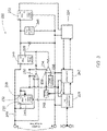
- the power management system 400 includes many of the elements presented and described for the power management circuit 222 presented in FIG. 3 and described in the above accompanying text. Therefore, for clarity of exposition, the differences between the elements of FIG. 3 and FIG. 4 are described below.
- the power management circuit 402 of the power management system 400 includes an energy pump 404 having an input 405 in electrical communication with the LIP 422 connector, a feedback input 403 for accepting a feedback sense from a control circuit, and an output 406 that provides a charging voltage to an energy storage element 226 and a voltage regulator 252.
- the energy pump 404 is a voltage converter that receives a first voltage and converts it to a higher (or lower) voltage.
- the energy pump 404 is selectively controlled by the control circuit 410 that modulates the feedback sense.
- the control circuit 410 comprises a feedback amplifier 407 that has two inputs 236, 238 connected to a reference voltage 237 and the output of a scaler 408.
- the control circuit 410 modulates the feedback sense at least in part based on the loop current in the control loop to regulate the insertion voltage between LIP 422 and LIN 424.
- the scaler 408 facilitates control of the insertion voltage by the microcontroller 247. This allows dynamic control of power management by the power management circuit 402.
- the loop insertion voltage can be regulated by balancing the energy extracted from the control loop with the energy available in the control loop. Because the current regulator 116 modulates the current in the control loop, for example between 4 mA and 20 mA, the amount of energy available in the control loop can change dynamically.
- the precise amount of energy transfer by the energy pump 404 is monitored by the feedback amplifier 407 that compares the reference voltage 237 against the insertion voltage and keeps the insertion voltage precise (DC voltage) and stable (AC noise.) No power from the control loop is wasted until the stored power in the energy storage element 226 reaches a maximum, resulting in efficient utilization of the available power in the control loop.
- the scaler 408 can be dynamically controlled by the microcontroller 247.
- the insertion voltage can be set to a higher than normal value, for example 2.5 Volts. Setting the insertion voltage higher enables a rapid deployment mode, whereby the energy storage element 226 can be quickly charged to full capacity. Setting the insertion voltage higher enables the energy pump 404 to transfer more power from the control loop. More power can be available from the energy pump 404 and energy storage element 226, and the microcontroller 247 can increase the radio 224 transmission parameters, increasing the transmission rate and enabling more frequent communications across the radio link.
- IS intrinsically safe
- the increased amount of power can allow the microcontroller 247 to run at a second operational mode, such as a high power mode.
- the scaler 408 can be a step-volt scaler, enabling insertion voltages at incremental steps between approximately 0.5 Volts and approximately 2.5 Volts in 0.5 Volt increments.
- the scaler 408 can be a digital or analogy scaler, enabling insertion voltages at various ranges and increments.
- the power management circuit 402 is connected in serial with a control loop of a controller 112, 212 and a field device 102, 202 (shown in FIG. 1 and FIG. 3 ). In this configuration, the power management circuit 402 is connected in serial with one of the control loop wires 108, 110, 208, 210 using the LIP 422 and LIN 424 connectors, as illustrated in FIG.2 .
- the power management circuit 402 can also be connected with a battery (not shown) that directly powers the field device 102, 202. In this configuration, there is no controller 112, 212. Instead, a first terminal of a battery, for example the positive terminal, is connected to the direct power input 420. The second terminal of the battery, for example the negative terminal, is connected to the LIN 424 connector. The first terminal of the battery is also connected to one of the connection terminals 104 of the field device 102. The other connection terminal 106 is in electrical communication with the HART connector 426.
- Current for the control loop flows from the first terminal of the battery through the field device 102, is modulated by current regulator 116, that can also be a voltage or power regulator, and returns to the power management circuit 402 through the HART connector 426, through the internal current sense resistor 418 and field device switch 416, and through the sense resistor 248 to the second terminal of the battery.
- current regulator 116 that can also be a voltage or power regulator
- the sense resistor 248 is a loop sense resistor in that it provides a way to produce a measurement of the amount of loop current in the control loop or current loop.
- the sense resistor 248 can be a low value resistor, for example a 1 Ohm resistor with a 1/4 Watt power rating.
- a loop current sense amplifier 409 connects to the sense resistor 248 and produces a loop current sense signal from the voltage drop, or loop current sense value, across the sense resistor 248.
- the loop current sense signal can be provided to the microcontroller 247.
- the loop current sense amplifier 409 can be connected through a blocking diode 413 to the feedback input 413 of the energy pump 404 to further modulate the feedback sense.
- a high value in the loop current sense signal indicates an unsafe or over-current condition for the power management circuit 402.
- the high value in the loop current sense signal can be configured to have a threshold that, when exceeded, shuts down the energy pump to prevent damage to the power management circuit 402.
- the voltage drop across the sense resistor 248 provides a loop current sense value directly correlating to the current in the control loop passing through the power management circuit 402 between the L1N 424 connector and L1P 422 connector.
- the current passing through the sense resistor 248 includes both the current in the control loop and the current drawn from the battery by the power management circuit 402.
- the microcontroller 247 selectively turns on and off the voltage converter 414. Note that the microcontroller 247 can be any kind of processor, CPU, ASIC, or processing logic and analog-to-digital converters, or combination of circuits.
- the voltage converter 414 When the voltage converter 414 is turned on, the voltage converter 414 provides an electric charging current directly to the energy storage element 226 and voltage regulator 252. A blocking diode 413 prevents power from flowing back into the voltage converter 414, for example when the energy pump 404 is turned on. The amount of current and power drawn by the voltage converter 414 is dependent upon the current draw of the power consuming circuits 225, 247, 224. For example, if the radio 224 is transmitting and receiving wireless data, the radio 224 can draw electrical power from the stored power in energy storage element 226 through the voltage regulator 252. In response, the voltage converter 414 can draw power from the battery to recharge the energy storage element 226 or to directly provide charging voltage to the voltage regulator 252.
- the electrical return to the battery for the current drawn by both the power management circuit 402 and the power consuming circuits 225, 247, 224 is through the sense resistor 248. Therefore, when the microcontroller 247 selectively turns on the voltage converter 414, the sense resistor provides a measure of the total consumption of power by the power management system 400 and field device.
- the energy storage element 226 is the source of electrical power for both the power management circuit 402 and the power consuming circuits 225, 247, 224.
- the voltage regulator 252 is off, the power management circuit 402 and power consuming circuits 225, 247, 224 are electrically isolated from the control loop and the sense resistor 248.
- the current flowing through the sense resistor 248 is the current in the control loop.
- the controller 247 can selectively turn on and off the voltage converter 414, perform measurements of the current flowing through the sense resistor 248, and obtain a diagnostic indication of the power usage in the power management system 400.
- the controller can 247 monitor the loop current flowing through the sense resistor 248 and selectively turn off components to reduce or disable the loop current.
- the controller 247 can disable the radio 224, the HART communications interface 225, and the voltage converter 414, and the controller 247 can also create an open circuit condition in the field device switch 416.
- the controller 247 can open the field device switch 416 if there is an electrical fault in the control loop, or if the power management circuit 402 is incorrectly connected to the battery or field device 102, 202.
- the controller can open the field device switch 416 to prevent damage to the power management system 400 in the event of a reverse connection of the battery, or an overvoltage condition, significantly reducing field return failures of components damaged by incorrect installation.
- the field device switch 416 can default to being open, allowing installation prior to powering the controller 247. Once powered, the controller 247 can momentarily close the field device switch 416 to test for incorrect connections or voltages without subjecting the rest of the power management circuit 402 to significant amounts of current.
- the field device switch 416 provides a current return path for the control loop through the internal current sense resistor 418, or current sense resistor.
- the internal current sense resistor 418 can be 250 Ohms.
- An internal current sense resistor 418 having a resistance of 250 Ohms provides the proper impedance characteristics for transmitting and receiving HART communications between the HART communications interface logic 225 and the field device 102, 202.
- the HART communications interface logic 225 is capacitively connected to the control loop.
- the capacitor 412 blocks the DC component of the while passing the FSK signal of the HART protocol. Note that the capacitor 412 can be connected to any point in the control loop.
- the controller 247 can open the field device switch 416 to remove power to the field device 102, 202 thereby placing the field device 102, 202 in a sleep mode.
- the controller 247 can close the field device switch 416 and wake the field device 102, 202 to retrieve the required information. Selectively removing power to the field device 102, 202 can substantially lengthen the useful life of a battery.
- the power management system 400 can intermittently and briefly power up the field device 102, 202 through the field device switch 416, communicate with the field device 102, 202 to obtain a control process data, power down the field device 102, 202, and send the data or information across a wireless network.
Landscapes
- Engineering & Computer Science (AREA)
- Power Engineering (AREA)
- Charge And Discharge Circuits For Batteries Or The Like (AREA)
- Arrangements For Transmission Of Measured Signals (AREA)
Claims (12)
- Système comprenant- un dispositif de terrain (102, 202),- une batterie en guise de source d'alimentation électrique (214) connectée électriquement au dispositif de terrain (102, 202), la source d'alimentation électrique (214) étant configurée pour transmettre un courant de boucle au dispositif de terrain (102, 202) et le dispositif de terrain (102, 202) étant configuré pour réguler le courant de boucle, et- un dispositif de communication sans fil (224) connecté électriquement à un circuit de gestion de puissance (222) et configuré pour recevoir l'alimentation électrique du circuit de gestion de puissance (222),- une pluralité de nœuds (L1N, L1P), ces nœuds étant connectés en série avec des fils de boucle de contrôle pour une connexion en série avec la boucle de contrôle pour une connexion en série avec le dispositif de terrain (102, 202),- le circuit de gestion de puissance (222) pouvant être connecté entre la pluralité de nœuds (L1N, L1P) et étant configuré pour être dans une connexion en série entre la source d'alimentation électrique (214) et le dispositif de terrain (102, 202) un flux de courant de boucle à travers le circuit de gestion de puissance (222) induisant une chute de tension régulée à travers les nœuds (L1N, L1P) à une tension d'insertion, le circuit de gestion de puissance (222) étant configuré pour émettre une puissance électrique dérivée de la tension d'insertion, le dispositif de terrain (102, 202) étant configuré pour recevoir une tension DC de la batterie,le circuit de gestion de puissance (222) comprenant- une pompe à énergie (404) configurée pour convertir la tension en une tension plus élevée ou plus basse, la pompe à énergie (404) étant configurée pour admettre au moins une partie de la tension d'insertion, la pompe à énergie (404) étant configurée pour recevoir une entrée de rétroaction, la pompe à énergie (404) étant configurée pour émettre une tension de charge basée au moins en partie sur l'entrée de rétroaction, la tension de charge étant configurée pour alimenter la sortie d'énergie électrique par le circuit de gestion de puissance (222),- un élément de stockage électrique (226) connecté électriquement à la pompe à énergie (404), l'élément de stockage électrique (226) étant configuré pour stocker la tension de charge comme énergie emmagasinée,- un régulateur de tension (252) connecté électriquement à l'élément de stockage électrique (226), le régulateur de tension (252) étant configuré pour réguler l'énergie emmagasinée et émettre la puissance électrique du circuit de gestion de puissance (222) et- un circuit de commande (410) configuré pour réguler la tension d'insertion en modulant l'entrée de rétroaction dans la pompe à énergie (404), le circuit de commande (410) étant configuré pour moduler l'entrée de rétroaction au moins partiellement en réponse à un changement électrique dans la boucle de courant, caractérisé en ce que le circuit de gestion de puissance (222) comprend en outre- un convertisseur de tension (414) configuré pour recevoir la tension DC de la batterie et envoyer la tension de charge au circuit de gestion de puissance (222),- dans lequel le convertisseur de tension et une première borne du dispositif de terrain sont connectés électriquement à une première borne de la batterie et dans lequel- le circuit de gestion de puissance comprend en outre une résistance de détection de boucle (248) connectée électriquement à une seconde borne de la batterie, la résistance de détection de boucle (248) étant configurée pour offrir une détection de courant de boucle d'un courant dans le circuit de gestion de puissance (222), et- un amplificateur de détection de courant de boucle (409) configuré pour recevoir la détection de courant de boucle et envoyer un signal de détection de courant de boucle,- une résistance de détection de courant (418) étant connectée à une seconde borne du dispositif de terrain (102, 202),- un processeur (247) faisant partie d'un circuit de consommation de puissance (225, 247, 224) et étant connecté électriquement à la résistance de détection de boucle (248) ainsi qu'au convertisseur de tension (414), le processeur (247) étant configuré pour recevoir le signal de détection de courant de boucle et pour activer et désactiver de façon sélective le convertisseur de tension (414) de telle sorte que, quand le convertisseur de tension (414) est désactivé, le courant dans le circuit de gestion de puissance (222) est approximativement un courant de boucle de la batterie en série avec le dispositif de terrain (102, 202), la résistance de détection de boucle (248) et la résistance de détection de courant (418), et- le circuit de consommation de puissance (225, 247, 224) étant configuré pour recevoir la puissance électrique du circuit de gestion de puissance (222).
- Système selon la revendication 1, dans lequel le circuit de consommation de puissance (225, 247, 224) est en outre sélectionné parmi le groupe constitué d'un dispositif de communication sans fil (224) et d'une interface de transducteur distant adressable par route (Highway Addressable Remote Transducer - HART) configurée pour communiquer avec le dispositif de terrain (102, 202) selon un protocole HART.
- Système selon la revendication 1, dans lequel l'élément de stockage électrique (226) comprend au moins un condensateur et une batterie.
- Système selon la revendication 1, dans lequel le circuit de gestion de puissance (222) comprend en outre un circuit de shuntage de tension (246) connecté électriquement à l'élément de stockage électrique (226), le circuit de shuntage de tension étant configuré pour empêcher un état de surtension de l'élément de stockage électrique (226).
- Système selon la revendication 1, dans lequel le circuit de commande (410) comprend en outre un amplificateur de rétroaction (407) configuré pour envoyer l'entrée de rétroaction à la pompe à énergie (404), comprenant une première entrée configurée pour recevoir une tension de référence (237), une seconde entrée (236) configurée pour recevoir une tension de rétroaction ayant une valeur en corrélation avec un multiple de la tension d'insertion et une sortie connectée électriquement à la pompe à énergie (404).
- Système selon la revendication 5, dans lequel le circuit de commande (410) comprend en outre un scaleur (108) configuré pour recevoir au moins une partie de la tension d'insertion et envoyer à la seconde entrée (236) de l'amplificateur de rétroaction (407) une tension de rétroaction qui est un multiple sélectionnable de la tension d'insertion, et dans lequel le processeur (247) est configuré pour contrôler le scaleur (108).
- Système selon la revendication 5, dans lequel l'amplificateur de détection de courant de boucle (409) est connecté électriquement à la pompe à énergie (404), et dans lequel le signal de détection de courant de boucle module en outre l'entrée de rétroaction pour désactiver la pompe à énergie (404) quand le courant dans le circuit de gestion de puissance (222) excède un seuil de surintensité, et dans lequel l'amplificateur de détection de courant de boucle (409) est configuré pour fournir un signal de détection de courant de boucle correspondant à un courant de boucle dans la boucle de courant, et dans lequel le processeur (247) est connecté électriquement à l'amplificateur de détection de courant de boucle (409) et le processeur (247) est configuré pour recevoir le signal de détection de courant de boucle, et dans lequel le processeur (247) est configuré pour fonctionner dans un mode de déploiement rapide en contrôlant le scaleur (108) et en augmentant la tension d'insertion quand un valeur du signal de détection de courant de boucle passe un seuil.
- Système selon la revendication 1, dans lequel le circuit de commande (410) est configuré pour réguler le courant continu d'environ 0,5 volt et le courant continu d'environ 2,5 volts, et comprenant en outre une interface HART configurée pour communiquer avec le dispositif de terrain (102, 202) selon un protocole HART, l'interface HART étant configurée pour être couplée de façon capacitive à la boucle de courant, et un commutateur de dispositif de terrain (416) configuré pour créer de façon sélective une situation de circuit ouvert pour la résistance de détection de courant (418), et dans lequel le processeur est configuré pour contrôler le commutateur de dispositif de terrain (416) pour créer de façon sélective la situation de circuit ouvert pour la résistance de détection de courant (418).
- Système selon la revendication 8, dans lequel le dispositif de terrain (102, 202) comprend un transducteur de tension.
- Système selon la revendication 9, comprenant en outre l'interface HART (225) configurée pour être couplée de façon capacitive à la boucle de courant, et dans lequel la source d'alimentation électrique (214) est une batterie.
- Procédé pour gérer la puissance d'un système selon la revendication 1 comprenant un dispositif de terrain (102, 202) et un dispositif de communication sans fil (224), ce procédé comprenant la réception d'une tension DC d'une batterie, la batterie étant configurée pour fournir un courant de boucle au dispositif de terrain (102, 202), la conversion de la tension DC en une tension de charge, la conversion étant désactivée de façon sélective pendant une opération de mesure d'un courant de boucle du dispositif de terrain (102, 202), l'envoi de la tension de charge à un élément de stockage électrique (226) et le stockage de la tension de charge comme une énergie emmagasinée dans l'élément de stockage électrique (226) pour la fournir au dispositif de communication sans fil (224).
- Procédé selon la revendication 11, comprenant en outre la désactivation du courant de boucle pour mettre le dispositif de terrain (102, 202) en mode de veille et l'activation du courant de boucle pour réveiller le dispositif de terrain (102, 202), et comprenant en outre la mesure du courant de boucle et la désactivation du courant de boucle quand le courant de boucle dépasse un seuil, comprenant en outre la régulation de l'énergie emmagasinée qui est fournie par l'élément de stockage électrique (226) au dispositif de communication sans fil (224), comprenant en outre la communication de données de contrôle de processus avec le dispositif de terrain (102, 202) utilisant un protocole HART, et comprenant en outre la communication des données de contrôle de processus avec une passerelle utilisant le dispositif de communication sans fil (224).
Applications Claiming Priority (2)
| Application Number | Priority Date | Filing Date | Title |
|---|---|---|---|
| US31703110P | 2010-03-24 | 2010-03-24 | |
| PCT/US2011/029877 WO2011119892A1 (fr) | 2010-03-24 | 2011-03-24 | Circuit de gestion de puissance pour un dispositif de communication sans fil et système de commande de procédé associé |
Publications (3)
| Publication Number | Publication Date |
|---|---|
| EP2567436A1 EP2567436A1 (fr) | 2013-03-13 |
| EP2567436A4 EP2567436A4 (fr) | 2015-10-07 |
| EP2567436B1 true EP2567436B1 (fr) | 2022-04-20 |
Family
ID=44673642
Family Applications (1)
| Application Number | Title | Priority Date | Filing Date |
|---|---|---|---|
| EP11760264.9A Active EP2567436B1 (fr) | 2010-03-24 | 2011-03-24 | Circuit de gestion de puissance pour un dispositif de communication sans fil et système de commande de procédé associé |
Country Status (4)
| Country | Link |
|---|---|
| US (2) | US9735570B2 (fr) |
| EP (1) | EP2567436B1 (fr) |
| CN (1) | CN103380556B (fr) |
| WO (1) | WO2011119892A1 (fr) |
Families Citing this family (30)
| Publication number | Priority date | Publication date | Assignee | Title |
|---|---|---|---|---|
| JP2012027832A (ja) * | 2010-07-27 | 2012-02-09 | Yokogawa Electric Corp | フィールド機器 |
| US20120253481A1 (en) * | 2011-03-29 | 2012-10-04 | General Electric Company | Hart channel interface component including redundancy |
| JP2014112819A (ja) | 2012-10-30 | 2014-06-19 | Yokogawa Electric Corp | 無線機器、入出力ユニット、無線ユニット、及び無線機器の設定方法 |
| DE102012112635B4 (de) * | 2012-12-19 | 2025-01-30 | Endress+Hauser Process Solutions Ag | Funkmodul für ein Feldgerät |
| WO2014146243A1 (fr) * | 2013-03-19 | 2014-09-25 | General Electric Company | Modulateur de tension de boucle de courant pour interface de communication |
| JP5898642B2 (ja) * | 2013-05-20 | 2016-04-06 | 横河電機株式会社 | 無線機器 |
| US9008197B2 (en) | 2013-07-26 | 2015-04-14 | General Electric Company | Current loop voltage modulator for communication interface |
| US20150194809A1 (en) * | 2014-01-07 | 2015-07-09 | Erick Mendoza | Variable DC Power Supply and HART Adapter |
| US10281939B2 (en) | 2014-02-17 | 2019-05-07 | Commscope Technologies Llc | Methods and equipment for reducing power loss in cellular systems |
| US11333695B2 (en) | 2014-02-17 | 2022-05-17 | Commscope Technologies Llc | Methods and equipment for reducing power loss in cellular systems |
| US9448576B2 (en) | 2014-02-17 | 2016-09-20 | Commscope Technologies Llc | Programmable power supplies for cellular base stations and related methods of reducing power loss in cellular systems |
| US9575132B2 (en) * | 2014-07-17 | 2017-02-21 | Honeywell International Inc. | Method and system for calculating accurate battery percentage usage in wireless field devices |
| WO2016032477A1 (fr) * | 2014-08-28 | 2016-03-03 | Ge Intelligent Platforms, Inc. | Procédé, système, et dispositif de couplage d'un signal de tension modulée à une boucle de courant au moyen d'un pont à impédance variable |
| US10110279B2 (en) * | 2014-10-07 | 2018-10-23 | Endress + Hauser Process Solutions Ag | Apparatus for supplying power to a field device |
| KR102341489B1 (ko) * | 2015-02-27 | 2021-12-21 | 삼성전자 주식회사 | 전자 장치 및 전자 장치의 충전 제어 방법 |
| US9615149B1 (en) * | 2015-10-26 | 2017-04-04 | Honeywell International Inc. | Process interface including wireless multi-loop single hop device |
| US10599134B2 (en) * | 2016-07-22 | 2020-03-24 | Fisher-Rosemount Systems, Inc. | Portable field maintenance tool configured for multiple process control communication protocols |
| US10476394B2 (en) * | 2016-12-28 | 2019-11-12 | Texas Instruments Incorporated | Dynamic learning of voltage source capabilities |
| SE1750548A1 (en) * | 2017-05-05 | 2018-11-06 | Fingerprint Cards Ab | Field-powered biometric device, and method of controlling a field-powered biometric device |
| KR101984140B1 (ko) * | 2017-05-12 | 2019-05-30 | 주식회사 맵스 | 전하 펌프 기반의 무선전력 수신기 |
| DE102017114851A1 (de) * | 2017-07-04 | 2019-01-10 | Endress+Hauser SE+Co. KG | Feldgeräteadapter zur drahtlosen Datenübertragung |
| DE102017121923B4 (de) * | 2017-09-21 | 2019-12-19 | Vega Grieshaber Kg | Messanordnung mit einem Bediengerät und Verfahren zum Betreiben einer solchen Messanordnung |
| US10531255B2 (en) | 2017-10-17 | 2020-01-07 | Honeywell International Inc. | Method and system for over-the-air provisioning of wireless HART (highway addressable remote transducer) devices |
| DE102018120108A1 (de) * | 2018-08-17 | 2020-02-20 | Endress+Hauser SE+Co. KG | Feldgerät der Automatisierungstechnik |
| DE102018122014A1 (de) | 2018-09-10 | 2020-03-12 | Endress + Hauser Flowtec Ag | Meßgeräte-System sowie damit gebildete Meßanordnung |
| US10892925B2 (en) * | 2018-11-16 | 2021-01-12 | Analog Devices International Unlimited Company | Communication receiver interface for current loop circuit |
| DE102019119840A1 (de) * | 2019-07-23 | 2021-01-28 | Endress+Hauser SE+Co. KG | Feldgerät der Automatisierungstechnik |
| DE102020105605A1 (de) * | 2020-03-03 | 2021-09-09 | Endress+Hauser SE+Co. KG | Feldgeräteadapter zur drahtlosen Datenübertragung |
| CN114552529B (zh) * | 2022-01-28 | 2022-10-21 | 绵阳惠科光电科技有限公司 | 过压保护电路、装置、显示面板及显示器 |
| DE102022119145A1 (de) * | 2022-07-29 | 2024-02-01 | Endress+Hauser Flowtec Ag | Anschlussschaltung für ein Feldgerät und Feldgerät |
Family Cites Families (31)
| Publication number | Priority date | Publication date | Assignee | Title |
|---|---|---|---|---|
| KR100285949B1 (ko) | 1996-12-12 | 2001-04-16 | 윤종용 | 배터리 충전회로 |
| US6167134A (en) * | 1997-04-22 | 2000-12-26 | Silicon Laboratories, Inc. | External resistor and method to minimize power dissipation in DC holding circuitry for a communication system |
| US5959372A (en) | 1997-07-21 | 1999-09-28 | Emerson Electric Co. | Power management circuit |
| US6870279B2 (en) | 1998-01-05 | 2005-03-22 | Capstone Turbine Corporation | Method and system for control of turbogenerator power and temperature |
| US6304978B1 (en) | 1998-11-24 | 2001-10-16 | Intel Corporation | Method and apparatus for control of the rate of change of current consumption of an electronic component |
| GB2357381B (en) | 1999-12-13 | 2003-12-24 | Sony Uk Ltd | Changing the output frequency of a phased-locked loop |
| US6574515B1 (en) | 2000-05-12 | 2003-06-03 | Rosemount Inc. | Two-wire field-mounted process device |
| DE60018072T2 (de) | 2000-10-27 | 2005-12-29 | Invensys Systems, Inc., Foxboro | Feldgerät mit einem Sender und/oder Empfänger zur drahtlosen Datenübertragung |
| WO2003036777A1 (fr) | 2001-10-22 | 2003-05-01 | Apple Computer, Inc. | Procedes et appareil de charge d'une batterie dans un dispositif peripherique |
| US6842383B2 (en) * | 2003-01-30 | 2005-01-11 | Saifun Semiconductors Ltd. | Method and circuit for operating a memory cell using a single charge pump |
| US7194363B2 (en) * | 2003-12-22 | 2007-03-20 | Endress + Hauser Flowtec Ag | Ultrasonic flowmeter |
| RU2347921C2 (ru) | 2004-03-02 | 2009-02-27 | Роузмаунт Инк. | Технологическое устройство с усовершенствованным обеспечением электропитанием |
| US8538560B2 (en) | 2004-04-29 | 2013-09-17 | Rosemount Inc. | Wireless power and communication unit for process field devices |
| US8145180B2 (en) * | 2004-05-21 | 2012-03-27 | Rosemount Inc. | Power generation for process devices |
| US8160535B2 (en) * | 2004-06-28 | 2012-04-17 | Rosemount Inc. | RF adapter for field device |
| US7262693B2 (en) | 2004-06-28 | 2007-08-28 | Rosemount Inc. | Process field device with radio frequency communication |
| JP4792851B2 (ja) | 2004-11-01 | 2011-10-12 | 横河電機株式会社 | フィールド機器 |
| US8050624B2 (en) | 2005-06-24 | 2011-11-01 | Rosemount, Inc. | Distributed process control system and method utilizing wireless communication of packet messages |
| RU2389056C2 (ru) * | 2005-06-27 | 2010-05-10 | Роузмаунт Инк. | Полевое устройство с радиочастотной связью, в которой потребляемая мощность динамически регулируется |
| WO2007021163A1 (fr) * | 2005-08-18 | 2007-02-22 | Cebt Co. Ltd. | Detecteur pour colonne electronique et procede permettant de detecter les electrons dans une colonne electronique |
| US7230528B2 (en) | 2005-09-20 | 2007-06-12 | Lawrence Kates | Programmed wireless sensor system |
| DE102005047894B4 (de) * | 2005-10-06 | 2010-05-12 | Abb Ag | Verfahren zur Prüfung der Betriebsfähigkeit von Messumformern |
| ATE453944T1 (de) * | 2005-12-13 | 2010-01-15 | Research In Motion Ltd | Batterieladegerät und stromversorgungsschaltung für mobile geräte |
| EP2162967B1 (fr) * | 2007-06-15 | 2020-03-04 | Fisher Controls International Llc | Convertisseur continu-continu à entrées régulées pour balayage d'énergie |
| CN101682259B (zh) | 2007-06-15 | 2014-06-25 | 费希尔控制产品国际有限公司 | 功率收集应用中用于功率储存控制的双向dc-dc转换器 |
| EP2165419B1 (fr) | 2007-06-26 | 2018-01-03 | Pepperl + Fuchs GmbH | Circuit de gestion de puissance pour un dispositif de communication sans fil et système de contrôle du processus utilisant celui-ci |
| WO2009003146A1 (fr) | 2007-06-26 | 2008-12-31 | Mactek Corporation | Systèmes de connexion de traversée et procédés de commande de traitement d'appareils de terrain |
| US20090094466A1 (en) * | 2007-10-04 | 2009-04-09 | Matthew Kerry R | Process field device with augmented loop power and wireless communication |
| CN102067048B (zh) | 2008-06-17 | 2017-03-08 | 罗斯蒙特公司 | 用于具有可变压降的现场设备的rf适配器 |
| CN102084307B (zh) * | 2008-06-17 | 2014-10-29 | 罗斯蒙特公司 | 用于具有低压本质安全钳的现场设备的rf适配器 |
| WO2011116362A1 (fr) * | 2010-03-18 | 2011-09-22 | Kenneth Burns | Modulation et démodulation par déplacement de fréquence |
-
2011
- 2011-03-24 WO PCT/US2011/029877 patent/WO2011119892A1/fr not_active Ceased
- 2011-03-24 US US13/699,107 patent/US9735570B2/en active Active
- 2011-03-24 CN CN201180026086.XA patent/CN103380556B/zh not_active Expired - Fee Related
- 2011-03-24 EP EP11760264.9A patent/EP2567436B1/fr active Active
-
2017
- 2017-07-07 US US15/644,251 patent/US10554043B2/en active Active
Also Published As
| Publication number | Publication date |
|---|---|
| EP2567436A4 (fr) | 2015-10-07 |
| CN103380556B (zh) | 2016-02-03 |
| US9735570B2 (en) | 2017-08-15 |
| WO2011119892A1 (fr) | 2011-09-29 |
| US20130082667A1 (en) | 2013-04-04 |
| US10554043B2 (en) | 2020-02-04 |
| US20170331286A1 (en) | 2017-11-16 |
| CN103380556A (zh) | 2013-10-30 |
| EP2567436A1 (fr) | 2013-03-13 |
Similar Documents
| Publication | Publication Date | Title |
|---|---|---|
| EP2567436B1 (fr) | Circuit de gestion de puissance pour un dispositif de communication sans fil et système de commande de procédé associé | |
| US9625895B2 (en) | Regulating power for a wireless communication device | |
| US9860093B2 (en) | Frequency shift keying modulation and demodulation | |
| US9818530B2 (en) | Adaptive wireless power transfer system and method | |
| US10567853B2 (en) | Smart grid appliance control | |
| CN103094952B (zh) | 控制装置、控制方法及控制系统 | |
| US20090207770A1 (en) | Apparatus and method for power management of wirelessly networked devices | |
| KR20180018741A (ko) | 어댑터 및 충전 제어 방법 | |
| CN107148708A (zh) | 数字电力接收器系统 | |
| WO2012007942A2 (fr) | Système de gestion de l'énergie et procédé de transfert inductif d'énergie | |
| CN213754015U (zh) | 一种蓝牙耳机的充电电路、充电盒及充电系统 | |
| EP3796504B1 (fr) | Système électrique et procédé de fonctionnement d'un tel système | |
| KR20190012985A (ko) | 무선 전력 송신기 및 무선 전력 송신기의 제어 방법 | |
| US10566833B2 (en) | External battery backup unit | |
| CN103094949A (zh) | 控制装置和控制方法 | |
| US20240154445A1 (en) | Intelligent bms charge control | |
| AU2016293631A1 (en) | Storage battery control system, storage battery control method, and program | |
| CN215731396U (zh) | 一种应用于自动转换开关的物联网转换电路 | |
| JP2016103890A (ja) | 電力制御装置および電力制御システム | |
| ES2664468T3 (es) | Circuito de gestión de potencia para un dispositivo de comunicación inalámbrica y un sistema de control de procedimiento que usa el mismo | |
| US20230120207A1 (en) | Controlling pulsed operation of a power supply during a power outage | |
| RU2574318C2 (ru) | Беспроводное полевое устройство со съемным источником электропитания |
Legal Events
| Date | Code | Title | Description |
|---|---|---|---|
| PUAI | Public reference made under article 153(3) epc to a published international application that has entered the european phase |
Free format text: ORIGINAL CODE: 0009012 |
|
| 17P | Request for examination filed |
Effective date: 20121218 |
|
| AK | Designated contracting states |
Kind code of ref document: A1 Designated state(s): AL AT BE BG CH CY CZ DE DK EE ES FI FR GB GR HR HU IE IS IT LI LT LU LV MC MK MT NL NO PL PT RO RS SE SI SK SM TR |
|
| RAP1 | Party data changed (applicant data changed or rights of an application transferred) |
Owner name: MACTEK CORPORATION |
|
| RIN1 | Information on inventor provided before grant (corrected) |
Inventor name: MACTEK CORPORATION |
|
| DAX | Request for extension of the european patent (deleted) | ||
| RA4 | Supplementary search report drawn up and despatched (corrected) |
Effective date: 20150904 |
|
| RIC1 | Information provided on ipc code assigned before grant |
Ipc: H02J 1/00 20060101ALI20150831BHEP Ipc: H02J 1/10 20060101AFI20150831BHEP Ipc: H02M 3/158 20060101ALI20150831BHEP Ipc: H02J 7/34 20060101ALI20150831BHEP |
|
| RAP1 | Party data changed (applicant data changed or rights of an application transferred) |
Owner name: PEPPERL+FUCHS GMBH |
|
| RIN1 | Information on inventor provided before grant (corrected) |
Inventor name: PEPPERL+FUCHS GMBH |
|
| STAA | Information on the status of an ep patent application or granted ep patent |
Free format text: STATUS: EXAMINATION IS IN PROGRESS |
|
| 17Q | First examination report despatched |
Effective date: 20180920 |
|
| RAP1 | Party data changed (applicant data changed or rights of an application transferred) |
Owner name: PEPPERL+FUCHS AG |
|
| RIN1 | Information on inventor provided before grant (corrected) |
Inventor name: PEPPERL+FUCHS AG |
|
| RAP1 | Party data changed (applicant data changed or rights of an application transferred) |
Owner name: PEPPERL+FUCHS SE |
|
| RIN1 | Information on inventor provided before grant (corrected) |
Inventor name: PEPPERL+FUCHS SE |
|
| REG | Reference to a national code |
Ref country code: DE Ref legal event code: R079 Ref document number: 602011072782 Country of ref document: DE Free format text: PREVIOUS MAIN CLASS: H02J0001100000 Ipc: H02J0001060000 |
|
| GRAP | Despatch of communication of intention to grant a patent |
Free format text: ORIGINAL CODE: EPIDOSNIGR1 |
|
| STAA | Information on the status of an ep patent application or granted ep patent |
Free format text: STATUS: GRANT OF PATENT IS INTENDED |
|
| RIC1 | Information provided on ipc code assigned before grant |
Ipc: G05B 19/042 20060101ALN20220125BHEP Ipc: H02J 7/34 20060101ALI20220125BHEP Ipc: H02J 1/10 20060101ALI20220125BHEP Ipc: H02J 1/06 20060101AFI20220125BHEP |
|
| GRAS | Grant fee paid |
Free format text: ORIGINAL CODE: EPIDOSNIGR3 |
|
| RIC1 | Information provided on ipc code assigned before grant |
Ipc: G05B 19/042 20060101ALN20220128BHEP Ipc: H02J 7/34 20060101ALI20220128BHEP Ipc: H02J 1/10 20060101ALI20220128BHEP Ipc: H02J 1/06 20060101AFI20220128BHEP |
|
| INTG | Intention to grant announced |
Effective date: 20220214 |
|
| GRAA | (expected) grant |
Free format text: ORIGINAL CODE: 0009210 |
|
| STAA | Information on the status of an ep patent application or granted ep patent |
Free format text: STATUS: THE PATENT HAS BEEN GRANTED |
|
| RIN1 | Information on inventor provided before grant (corrected) |
Inventor name: SINREICH, MARK |
|
| AK | Designated contracting states |
Kind code of ref document: B1 Designated state(s): AL AT BE BG CH CY CZ DE DK EE ES FI FR GB GR HR HU IE IS IT LI LT LU LV MC MK MT NL NO PL PT RO RS SE SI SK SM TR |
|
| REG | Reference to a national code |
Ref country code: GB Ref legal event code: FG4D |
|
| REG | Reference to a national code |
Ref country code: CH Ref legal event code: EP |
|
| REG | Reference to a national code |
Ref country code: DE Ref legal event code: R096 Ref document number: 602011072782 Country of ref document: DE |
|
| REG | Reference to a national code |
Ref country code: IE Ref legal event code: FG4D |
|
| REG | Reference to a national code |
Ref country code: AT Ref legal event code: REF Ref document number: 1485957 Country of ref document: AT Kind code of ref document: T Effective date: 20220515 |
|
| REG | Reference to a national code |
Ref country code: LT Ref legal event code: MG9D |
|
| REG | Reference to a national code |
Ref country code: NL Ref legal event code: MP Effective date: 20220420 |
|
| REG | Reference to a national code |
Ref country code: AT Ref legal event code: MK05 Ref document number: 1485957 Country of ref document: AT Kind code of ref document: T Effective date: 20220420 |
|
| PG25 | Lapsed in a contracting state [announced via postgrant information from national office to epo] |
Ref country code: NL Free format text: LAPSE BECAUSE OF FAILURE TO SUBMIT A TRANSLATION OF THE DESCRIPTION OR TO PAY THE FEE WITHIN THE PRESCRIBED TIME-LIMIT Effective date: 20220420 |
|
| PG25 | Lapsed in a contracting state [announced via postgrant information from national office to epo] |
Ref country code: SE Free format text: LAPSE BECAUSE OF FAILURE TO SUBMIT A TRANSLATION OF THE DESCRIPTION OR TO PAY THE FEE WITHIN THE PRESCRIBED TIME-LIMIT Effective date: 20220420 Ref country code: PT Free format text: LAPSE BECAUSE OF FAILURE TO SUBMIT A TRANSLATION OF THE DESCRIPTION OR TO PAY THE FEE WITHIN THE PRESCRIBED TIME-LIMIT Effective date: 20220822 Ref country code: NO Free format text: LAPSE BECAUSE OF FAILURE TO SUBMIT A TRANSLATION OF THE DESCRIPTION OR TO PAY THE FEE WITHIN THE PRESCRIBED TIME-LIMIT Effective date: 20220720 Ref country code: LT Free format text: LAPSE BECAUSE OF FAILURE TO SUBMIT A TRANSLATION OF THE DESCRIPTION OR TO PAY THE FEE WITHIN THE PRESCRIBED TIME-LIMIT Effective date: 20220420 Ref country code: HR Free format text: LAPSE BECAUSE OF FAILURE TO SUBMIT A TRANSLATION OF THE DESCRIPTION OR TO PAY THE FEE WITHIN THE PRESCRIBED TIME-LIMIT Effective date: 20220420 Ref country code: GR Free format text: LAPSE BECAUSE OF FAILURE TO SUBMIT A TRANSLATION OF THE DESCRIPTION OR TO PAY THE FEE WITHIN THE PRESCRIBED TIME-LIMIT Effective date: 20220721 Ref country code: FI Free format text: LAPSE BECAUSE OF FAILURE TO SUBMIT A TRANSLATION OF THE DESCRIPTION OR TO PAY THE FEE WITHIN THE PRESCRIBED TIME-LIMIT Effective date: 20220420 Ref country code: ES Free format text: LAPSE BECAUSE OF FAILURE TO SUBMIT A TRANSLATION OF THE DESCRIPTION OR TO PAY THE FEE WITHIN THE PRESCRIBED TIME-LIMIT Effective date: 20220420 Ref country code: BG Free format text: LAPSE BECAUSE OF FAILURE TO SUBMIT A TRANSLATION OF THE DESCRIPTION OR TO PAY THE FEE WITHIN THE PRESCRIBED TIME-LIMIT Effective date: 20220720 Ref country code: AT Free format text: LAPSE BECAUSE OF FAILURE TO SUBMIT A TRANSLATION OF THE DESCRIPTION OR TO PAY THE FEE WITHIN THE PRESCRIBED TIME-LIMIT Effective date: 20220420 |
|
| PG25 | Lapsed in a contracting state [announced via postgrant information from national office to epo] |
Ref country code: RS Free format text: LAPSE BECAUSE OF FAILURE TO SUBMIT A TRANSLATION OF THE DESCRIPTION OR TO PAY THE FEE WITHIN THE PRESCRIBED TIME-LIMIT Effective date: 20220420 Ref country code: PL Free format text: LAPSE BECAUSE OF FAILURE TO SUBMIT A TRANSLATION OF THE DESCRIPTION OR TO PAY THE FEE WITHIN THE PRESCRIBED TIME-LIMIT Effective date: 20220420 Ref country code: LV Free format text: LAPSE BECAUSE OF FAILURE TO SUBMIT A TRANSLATION OF THE DESCRIPTION OR TO PAY THE FEE WITHIN THE PRESCRIBED TIME-LIMIT Effective date: 20220420 Ref country code: IS Free format text: LAPSE BECAUSE OF FAILURE TO SUBMIT A TRANSLATION OF THE DESCRIPTION OR TO PAY THE FEE WITHIN THE PRESCRIBED TIME-LIMIT Effective date: 20220820 |
|
| REG | Reference to a national code |
Ref country code: DE Ref legal event code: R097 Ref document number: 602011072782 Country of ref document: DE |
|
| PG25 | Lapsed in a contracting state [announced via postgrant information from national office to epo] |
Ref country code: SM Free format text: LAPSE BECAUSE OF FAILURE TO SUBMIT A TRANSLATION OF THE DESCRIPTION OR TO PAY THE FEE WITHIN THE PRESCRIBED TIME-LIMIT Effective date: 20220420 Ref country code: SK Free format text: LAPSE BECAUSE OF FAILURE TO SUBMIT A TRANSLATION OF THE DESCRIPTION OR TO PAY THE FEE WITHIN THE PRESCRIBED TIME-LIMIT Effective date: 20220420 Ref country code: RO Free format text: LAPSE BECAUSE OF FAILURE TO SUBMIT A TRANSLATION OF THE DESCRIPTION OR TO PAY THE FEE WITHIN THE PRESCRIBED TIME-LIMIT Effective date: 20220420 Ref country code: EE Free format text: LAPSE BECAUSE OF FAILURE TO SUBMIT A TRANSLATION OF THE DESCRIPTION OR TO PAY THE FEE WITHIN THE PRESCRIBED TIME-LIMIT Effective date: 20220420 Ref country code: DK Free format text: LAPSE BECAUSE OF FAILURE TO SUBMIT A TRANSLATION OF THE DESCRIPTION OR TO PAY THE FEE WITHIN THE PRESCRIBED TIME-LIMIT Effective date: 20220420 Ref country code: CZ Free format text: LAPSE BECAUSE OF FAILURE TO SUBMIT A TRANSLATION OF THE DESCRIPTION OR TO PAY THE FEE WITHIN THE PRESCRIBED TIME-LIMIT Effective date: 20220420 |
|
| PLBE | No opposition filed within time limit |
Free format text: ORIGINAL CODE: 0009261 |
|
| STAA | Information on the status of an ep patent application or granted ep patent |
Free format text: STATUS: NO OPPOSITION FILED WITHIN TIME LIMIT |
|
| 26N | No opposition filed |
Effective date: 20230123 |
|
| PG25 | Lapsed in a contracting state [announced via postgrant information from national office to epo] |
Ref country code: AL Free format text: LAPSE BECAUSE OF FAILURE TO SUBMIT A TRANSLATION OF THE DESCRIPTION OR TO PAY THE FEE WITHIN THE PRESCRIBED TIME-LIMIT Effective date: 20220420 |
|
| PG25 | Lapsed in a contracting state [announced via postgrant information from national office to epo] |
Ref country code: SI Free format text: LAPSE BECAUSE OF FAILURE TO SUBMIT A TRANSLATION OF THE DESCRIPTION OR TO PAY THE FEE WITHIN THE PRESCRIBED TIME-LIMIT Effective date: 20220420 |
|
| PG25 | Lapsed in a contracting state [announced via postgrant information from national office to epo] |
Ref country code: MC Free format text: LAPSE BECAUSE OF FAILURE TO SUBMIT A TRANSLATION OF THE DESCRIPTION OR TO PAY THE FEE WITHIN THE PRESCRIBED TIME-LIMIT Effective date: 20220420 |
|
| GBPC | Gb: european patent ceased through non-payment of renewal fee |
Effective date: 20230324 |
|
| REG | Reference to a national code |
Ref country code: BE Ref legal event code: MM Effective date: 20230331 |
|
| PG25 | Lapsed in a contracting state [announced via postgrant information from national office to epo] |
Ref country code: LU Free format text: LAPSE BECAUSE OF NON-PAYMENT OF DUE FEES Effective date: 20230324 |
|
| REG | Reference to a national code |
Ref country code: IE Ref legal event code: MM4A |
|
| PG25 | Lapsed in a contracting state [announced via postgrant information from national office to epo] |
Ref country code: GB Free format text: LAPSE BECAUSE OF NON-PAYMENT OF DUE FEES Effective date: 20230324 |
|
| PG25 | Lapsed in a contracting state [announced via postgrant information from national office to epo] |
Ref country code: IT Free format text: LAPSE BECAUSE OF FAILURE TO SUBMIT A TRANSLATION OF THE DESCRIPTION OR TO PAY THE FEE WITHIN THE PRESCRIBED TIME-LIMIT Effective date: 20220420 Ref country code: IE Free format text: LAPSE BECAUSE OF NON-PAYMENT OF DUE FEES Effective date: 20230324 Ref country code: GB Free format text: LAPSE BECAUSE OF NON-PAYMENT OF DUE FEES Effective date: 20230324 Ref country code: FR Free format text: LAPSE BECAUSE OF NON-PAYMENT OF DUE FEES Effective date: 20230331 |
|
| PG25 | Lapsed in a contracting state [announced via postgrant information from national office to epo] |
Ref country code: BE Free format text: LAPSE BECAUSE OF NON-PAYMENT OF DUE FEES Effective date: 20230331 |
|
| PG25 | Lapsed in a contracting state [announced via postgrant information from national office to epo] |
Ref country code: BG Free format text: LAPSE BECAUSE OF FAILURE TO SUBMIT A TRANSLATION OF THE DESCRIPTION OR TO PAY THE FEE WITHIN THE PRESCRIBED TIME-LIMIT Effective date: 20220420 |
|
| PG25 | Lapsed in a contracting state [announced via postgrant information from national office to epo] |
Ref country code: BG Free format text: LAPSE BECAUSE OF FAILURE TO SUBMIT A TRANSLATION OF THE DESCRIPTION OR TO PAY THE FEE WITHIN THE PRESCRIBED TIME-LIMIT Effective date: 20220420 |
|
| PGFP | Annual fee paid to national office [announced via postgrant information from national office to epo] |
Ref country code: DE Payment date: 20250319 Year of fee payment: 15 |
|
| PGFP | Annual fee paid to national office [announced via postgrant information from national office to epo] |
Ref country code: CH Payment date: 20250401 Year of fee payment: 15 |
|
| PG25 | Lapsed in a contracting state [announced via postgrant information from national office to epo] |
Ref country code: CY Free format text: LAPSE BECAUSE OF FAILURE TO SUBMIT A TRANSLATION OF THE DESCRIPTION OR TO PAY THE FEE WITHIN THE PRESCRIBED TIME-LIMIT; INVALID AB INITIO Effective date: 20110324 |
|
| PG25 | Lapsed in a contracting state [announced via postgrant information from national office to epo] |
Ref country code: HU Free format text: LAPSE BECAUSE OF FAILURE TO SUBMIT A TRANSLATION OF THE DESCRIPTION OR TO PAY THE FEE WITHIN THE PRESCRIBED TIME-LIMIT; INVALID AB INITIO Effective date: 20110324 |
|
| PG25 | Lapsed in a contracting state [announced via postgrant information from national office to epo] |
Ref country code: TR Free format text: LAPSE BECAUSE OF FAILURE TO SUBMIT A TRANSLATION OF THE DESCRIPTION OR TO PAY THE FEE WITHIN THE PRESCRIBED TIME-LIMIT Effective date: 20220420 |