EP2568301B1 - Stromsensor und Leiterplatte für einen solchen Sensor - Google Patents
Stromsensor und Leiterplatte für einen solchen Sensor Download PDFInfo
- Publication number
- EP2568301B1 EP2568301B1 EP12183231.5A EP12183231A EP2568301B1 EP 2568301 B1 EP2568301 B1 EP 2568301B1 EP 12183231 A EP12183231 A EP 12183231A EP 2568301 B1 EP2568301 B1 EP 2568301B1
- Authority
- EP
- European Patent Office
- Prior art keywords
- coils
- coil
- pair
- printed circuit
- vertical
- Prior art date
- Legal status (The legal status is an assumption and is not a legal conclusion. Google has not performed a legal analysis and makes no representation as to the accuracy of the status listed.)
- Not-in-force
Links
Images


Classifications
-
- H—ELECTRICITY
- H05—ELECTRIC TECHNIQUES NOT OTHERWISE PROVIDED FOR
- H05K—PRINTED CIRCUITS; CASINGS OR CONSTRUCTIONAL DETAILS OF ELECTRIC APPARATUS; MANUFACTURE OF ASSEMBLAGES OF ELECTRICAL COMPONENTS
- H05K1/00—Printed circuits
- H05K1/16—Printed circuits incorporating printed electric components, e.g. printed resistors, capacitors or inductors
- H05K1/165—Printed circuits incorporating printed electric components, e.g. printed resistors, capacitors or inductors incorporating printed inductors
-
- G—PHYSICS
- G01—MEASURING; TESTING
- G01R—MEASURING ELECTRIC VARIABLES; MEASURING MAGNETIC VARIABLES
- G01R15/00—Details of measuring arrangements of the types provided for in groups G01R17/00 - G01R29/00, G01R33/00 - G01R33/26 or G01R35/00
- G01R15/14—Adaptations providing voltage or current isolation, e.g. for high-voltage or high-current networks
- G01R15/18—Adaptations providing voltage or current isolation, e.g. for high-voltage or high-current networks using inductive devices, e.g. transformers
- G01R15/183—Adaptations providing voltage or current isolation, e.g. for high-voltage or high-current networks using inductive devices, e.g. transformers using transformers with a magnetic core
- G01R15/185—Adaptations providing voltage or current isolation, e.g. for high-voltage or high-current networks using inductive devices, e.g. transformers using transformers with a magnetic core with compensation or feedback windings or interacting coils, e.g. 0-flux sensors
-
- H—ELECTRICITY
- H05—ELECTRIC TECHNIQUES NOT OTHERWISE PROVIDED FOR
- H05K—PRINTED CIRCUITS; CASINGS OR CONSTRUCTIONAL DETAILS OF ELECTRIC APPARATUS; MANUFACTURE OF ASSEMBLAGES OF ELECTRICAL COMPONENTS
- H05K1/00—Printed circuits
- H05K1/02—Details
- H05K1/0213—Electrical arrangements not otherwise provided for
- H05K1/0237—High frequency adaptations
- H05K1/0239—Signal transmission by AC coupling
-
- H—ELECTRICITY
- H05—ELECTRIC TECHNIQUES NOT OTHERWISE PROVIDED FOR
- H05K—PRINTED CIRCUITS; CASINGS OR CONSTRUCTIONAL DETAILS OF ELECTRIC APPARATUS; MANUFACTURE OF ASSEMBLAGES OF ELECTRICAL COMPONENTS
- H05K2201/00—Indexing scheme relating to printed circuits covered by H05K1/00
- H05K2201/08—Magnetic details
- H05K2201/083—Magnetic materials
- H05K2201/086—Magnetic materials for inductive purposes, e.g. printed inductor with ferrite core
-
- H—ELECTRICITY
- H05—ELECTRIC TECHNIQUES NOT OTHERWISE PROVIDED FOR
- H05K—PRINTED CIRCUITS; CASINGS OR CONSTRUCTIONAL DETAILS OF ELECTRIC APPARATUS; MANUFACTURE OF ASSEMBLAGES OF ELECTRICAL COMPONENTS
- H05K2201/00—Indexing scheme relating to printed circuits covered by H05K1/00
- H05K2201/09—Shape and layout
- H05K2201/09209—Shape and layout details of conductors
- H05K2201/09218—Conductive traces
- H05K2201/09263—Meander
-
- H—ELECTRICITY
- H05—ELECTRIC TECHNIQUES NOT OTHERWISE PROVIDED FOR
- H05K—PRINTED CIRCUITS; CASINGS OR CONSTRUCTIONAL DETAILS OF ELECTRIC APPARATUS; MANUFACTURE OF ASSEMBLAGES OF ELECTRICAL COMPONENTS
- H05K2201/00—Indexing scheme relating to printed circuits covered by H05K1/00
- H05K2201/09—Shape and layout
- H05K2201/09209—Shape and layout details of conductors
- H05K2201/09654—Shape and layout details of conductors covering at least two types of conductors provided for in H05K2201/09218 - H05K2201/095
- H05K2201/09672—Superposed layout, i.e. in different planes
-
- H—ELECTRICITY
- H05—ELECTRIC TECHNIQUES NOT OTHERWISE PROVIDED FOR
- H05K—PRINTED CIRCUITS; CASINGS OR CONSTRUCTIONAL DETAILS OF ELECTRIC APPARATUS; MANUFACTURE OF ASSEMBLAGES OF ELECTRICAL COMPONENTS
- H05K2201/00—Indexing scheme relating to printed circuits covered by H05K1/00
- H05K2201/09—Shape and layout
- H05K2201/09209—Shape and layout details of conductors
- H05K2201/09654—Shape and layout details of conductors covering at least two types of conductors provided for in H05K2201/09218 - H05K2201/095
- H05K2201/097—Alternating conductors, e.g. alternating different shaped pads, twisted pairs; Alternating components
-
- H—ELECTRICITY
- H05—ELECTRIC TECHNIQUES NOT OTHERWISE PROVIDED FOR
- H05K—PRINTED CIRCUITS; CASINGS OR CONSTRUCTIONAL DETAILS OF ELECTRIC APPARATUS; MANUFACTURE OF ASSEMBLAGES OF ELECTRICAL COMPONENTS
- H05K3/00—Apparatus or processes for manufacturing printed circuits
- H05K3/46—Manufacturing multilayer circuits
Definitions
- the invention relates to a current sensor and a printed circuit for producing this current sensor.
- a printed circuit also better known by the acronym PCB (Printed Circuit Board) is a support for electrically connecting a set of electrical components.
- Such a printed circuit is generally in the form of a laminated plate.
- This printed circuit can be monolayer or multilayer.
- a single-layer printed circuit comprises only one metallization layer in which conductive tracks are printed which electrically connect the different electrical components to each other.
- a multilayer printed circuit comprises several metallization layers, that is to say at least two layers and, preferably, more than four or six layers. In the remainder of this description, we are mainly interested in these multilayer printed circuits.
- a metallization layer is one of the layers of the laminated plate forming the printed circuit in which one or more conductive tracks are formed which electrically connect the different electrical components to one another. This layer is flat and extends parallel to the plane of the laminated plate.
- the metallization layer is obtained by depositing a uniform layer of a conductive material, typically a metal such as copper, then etching this uniform layer to leave only the conductive tracks.
- the various layers of metallization of the printed circuit are mechanically spaced from each other by insulating layers of electrically insulating material.
- This insulating material has a high dielectric strength that is to say typically greater than 3 MV / m and preferably greater than 10 MV / m.
- the electrically insulating material is made from epoxy resin and / or fiberglass.
- the insulating layer is generally in the form of a rigid plate made of a material that does not become viscous when it is assembled with other layers. For example, it is made from a thermosetting resin that has already undergone irreversible thermosetting.
- prepreg adhesive layers
- a prepreg consists of a thermosetting resin impregnating, usually a reinforcement such as a fabric.
- the resin is an epoxy resin.
- the transformation of the thermosetting resin involves an irreversible polymerization which transforms the prepreg in a solid and rigid material which bonds irreversibly between the different layers of the printed circuit.
- each transformation occurs when the prepreg is heated to a high temperature and is compressed with high pressure.
- a high temperature is a temperature above 100 ° C and preferably above 150 ° C.
- High pressure is a pressure greater than 0.3 MPa and typically greater than 1 MPa.
- the conductive tracks of the different metallization layers may be electrically connected via conductive pads passing through the insulating layers. Conductive pads are better known by the term "vias".
- the vias generally extend perpendicular to the plane of the layers. There are different ways to make these vias. One of the most common is to make a hole in the insulation or insulation to cross and then cover with a metal the inner wall of these holes. We then speak of metallized holes.
- a via does not necessarily cross all the layers of the printed circuit. Thus, there are blind vias that open on one side of the circuit board.
- HDI High Density of Integration
- a buried via does not lead to any of the outer faces of the printed circuit. For example, a buried via makes it possible to electrically connect conductive tracks made in metallization layers buried inside the printed circuit.
- the measuring and excitation coils are each made in a single metallization layer. Because of this, these coils are called "planar". To form the turns of these coils, each coil describes a spiral in a metallization layer.
- the invention therefore relates to a current sensor in which the turns of each coil are formed by conductive tracks, made in respective metallization layers, electrically connected to each other by studs passing through at least one of the layers insulators to form the coil that extends along the vertical axis.
- the current sensor above uses "vertical" coils, that is, coils that extend and wind along a vertical winding axis. For the same number of turns, a vertical coil captures or generates a magnetic field more homogeneous than that of a planar coil. Therefore, the above sensor is more accurate.
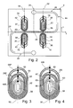
- the figure 1 illustrates a current sensor 2. This illustration has only been made to explain the operation of the sensor. Examples of more detailed embodiments of this sensor are described below.
- the sensor 2 comprises a printed circuit 4 and an electronic processing unit 6.
- the printed circuit 4 is a multilayer printed circuit whose metallization layers are horizontal.
- the printed circuit 4 comprises a line 10 in which the current to be measured flows.
- a line 10 in which the current to be measured flows.
- transverse sections 12, 14 of this line 10 are shown. These cross sections are two successive cross sections of the line 10.
- Line 10 generates a magnetic field Bi whose field lines form circles around the streamline.
- the magnetic fields B i at two points on either side of the line 10 and at the same distance from this line 10 are equal in amplitude but opposite in direction.
- the amplitude of the magnetic field B i is a function of the intensity of the current i flowing in line 10.
- the printed circuit 4 also comprises two pairs of coils.
- the first pair is formed of two measuring coils 16, 18.
- the coils 16, 18 are wound respectively around vertical axes 20 and 22 perpendicular to the plane of the metallization layers of the printed circuit 4. These coils 16 and 18 are identical except that they are arranged on either side of the line 10.
- the coils 16 and 18 are symmetrical to one another with respect to a vertical plane 24 passing through the line 10.
- the turns of the coils 16 and 18 are wound around a saturable magnetic core .
- This magnetic core has not been represented on the figure 1 .
- the magnetic core is a magnetic core made of ferromagnetic material whose static relative permeability, that is to say for a zero frequency, is very high.
- the relative static permeability is greater than 1000 and preferably greater than 10000 or 100000.
- the magnetic core is made of a material such as a mu-metal or a magnetic material known under the trade name Vitrovac® 6025.
- each coil 16, 18 has more than two turns and preferably more than three or six turns piled one above the other in the vertical direction.
- the magnetic field measured by the coils 16 and 18 are noted, respectively, M 1 and M 2 in the remainder of this description.
- the second pair of measuring coils is the symmetrical of the first pair with respect to a vertical plane perpendicular to the plane 24.
- the second pair is located downstream or upstream of the first pair along the line 10.
- the The measuring coils of this second pair carry, respectively, the references 26 and 28.
- the vertical axes around which the coils 26 and 28 are wound bear, respectively, the references 30 and 32.
- the printed circuit board 4 also comprises four excitation coils 36, 38, 40 and 42. These coils 36, 38, 40 and 42 are each formed of several coils wound respectively around the axes 20, 22, 30 and 32. Typically the number of turns of each excitation coil stacked one above the other in the vertical direction is greater than or equal to two and preferably greater than or equal to three or six.
- each excitation coil is concentric with a respective measuring coil.
- concentric is meant that the turns of each of these coils are made in the same metallization layer and wind around the same winding axis. Preferably, all the turns of a concentric coil are made in the same metallization layers than the turns of the other coil which is concentric to it.
- the measuring coils are wound around the excitation coils. To clarify the figure 1 , the coils 36 to 42 are shown next to the measuring coils with which they are associated.
- the excitation coils are symmetrical to each other with respect to the planes 24 and 25 as for the measuring coils. They are electrically connected in series in this embodiment. Thus, each excitation coil generates a magnetic field B ex of the same amplitude in the magnetic core of the measuring coil with which it is associated. More precisely, the coils 38 and 40 are electrically connected so as to both generate a field B ex of the same direction while the excitation coils 36 and 42 are connected so as to generate a magnetic field B ex in an opposite direction. .
- "connect” refers to the fact of electrically connecting.
- homogeneous magnetic field it is meant that this field T has the same direction and the same amplitude at any point of the printed circuit 4.
- this magnetic field T is the earth's magnetic field.
- the measuring coils 16, 18, 26 and 28 are electrically connected to each other so as to make the previous sum. Thus, only the result of this sum is transmitted to unit 6.
- the unit 6 is able to automatically compensate for the contributions of the magnetic fields B ex and T.
- the unit 6 also generates the excitation current.
- the unit 6 is made from an integrated electronic circuit.
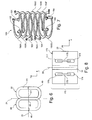
- the figure 2 is a metallization layer of the printed circuit 4.
- the printed circuit 4 is formed by a stack, in a vertical direction Z, of seven metallization layers each extending in a horizontal plane parallel to orthogonal directions X and Y.
- the layer metallization represented is an intermediate metallization layer, that is to say between upper and lower metallization layers forming, respectively, the upper and lower faces of the circuit 4. In the remainder of this description, the upper faces and lower are not shown in the figures.
- the segment 46 passes through vertical planes 50 and 52.
- the plane 50 is the plane that contains the axes 30 and 32 while the plane 52 is the plane that contains the vertical axes 20 and 22.
- the segment 46 is perpendicular to the planes 50 and 52.
- the direction through which planes 50 and 52 pass through line 10 corresponds to the direction of the current flowing through it when line 10 is fed by a direct current.
- the loop portions 48 and 49 are arranged so that the current flowing in each segment of the line 10 always crosses the planes 50 and 52 in the same direction. They make it possible to reduce the current flowing in an upper segment of the line 10 towards a segment below. These loop portions 48 to 49 do not do not pass between the axes 20 and 22 nor between the axes 30 and 32. For this, they circumvent from the outside the measuring coils.
- the outside is here defined as being the region of the printed circuit 4 which is opposite the side of the measuring coils closest to the plane 24.
- Line 10 is described in more detail with reference to the figure 6 .
- the two pairs of measuring coils are arranged one after the other in a direction Y along which segments 46 extend.
- the circuit 4 also comprises four holes 54, 56, 58 and 60 vertically crossing and through the circuit 4. These holes are intended to receive magnetic cores. An example of such a magnetic core is shown on the figure 5 . These holes are dug along the vertical axes, respectively, 20, 22, 30 and 32. These holes are oblong. The largest widths of the holes 54 and 56 are included in the plane 52 and the largest widths of the holes 58, 60 are included in the plane 50.
- the Figures 3 and 4 show in more detail the conductive tracks of the coils 26 and 40 made, respectively, in even and odd intermediate metallization layers. These coils are here formed by stacking, alternately, the even and odd metallization layers one above the other in the Z direction.
- the conductive tracks bear the same reference as the coil but followed by a " P "for the even metallization layer and an” I “for the odd metallization layer.
- the ends of the conductive tracks terminate either by a point or by a circle. The point and circle represent the ends, respectively, lower and upper of a via.
- the track 40P winds from a via 62 around the hole 58 to a via 63 going from the inside to the outside in the counter-clockwise direction.
- the track 26P wraps around the track 40P from a via 64 to a via 65 going from the inside to the outside in the counterclockwise direction.
- the track 401 wraps from the via 63 to a via 66 around the hole 58 from the outside to the inside in the counter-clockwise direction.
- Runway 261 wraps from via 65 to a via 67 around runway 401 from the outside to the inside in a counter-clockwise direction.
- tracks 68P and 681 of a compensation coil have also been shown. These tracks wind around the tracks of the measuring coil.
- the compensation coil makes it possible to generate a magnetic field which cancels the magnetic field in the introduced magnetic core In these conditions, the intensity of the current flowing in the line 10 is deduced from the intensity of the current supplying the coil 68. This makes it possible in particular to work in a zero field in the magnetic core.
- the tracks 261, 401 and 601 are deduced from the tracks 26P, 40P and 68P by axial symmetry with respect to the plane 50.
- the superposition, in the same horizontal plane, of the conductive tracks of the metallization layers pair and odd form a pattern having axial symmetry along an axis contained in the plane 50.
- the vias 62 to 67 are all contained in the plan 50.
- the compensation coil is similar to that of measurement and will therefore not be described in more detail.
- the tracks of the other coils 16, 18, 28, 36, 38, 42 are deduced from the tracks of the coils 26 and 40 by symmetry with respect to the planes 24 and 25.
- the figure 5 shows in more detail and in an exploded view the stacking of the different layers of the printed circuit 4.
- the printed circuit 4 comprises seven intermediate metallization layers 70 to 76 mechanically separated by insulating layers, respectively, 80 to 85.
- the conductive tracks are formed in each of the metallization layers 70 to 76 to form the line 10, the measurement coils 26 and 28 and the excitation coils 40 and 42.
- the printed circuit is shown in section along the plane 50.
- the turns of a spool bear the reference of that spool followed by the letters A, B, C, D, E, F and G from the upper end turn to the lower end turn.
- the turns whose references end in A, B, C, D, E, F and G are carried out, respectively, in the metallization layers 70, 71, 72, 73, 74, 75 and 76.
- the tracks of each coil are connected in series via vertical vias not shown in this figure. To simplify this figure, the conductive tracks of the same coil are represented by simple rectangles even if the track makes several turns around the holes 58 and 60.
- the segments 46, 101 to 106 and the loop portions 48, 110 to 116 are made, respectively, in the layers 70 to 76.
- the segments 46, 101 to 106 are stacked one above the other in the Z direction. They are also symmetrical with respect to the plane 24.
- the figure 5 also represents the magnetic core 120 housed in the holes 58 and 60.
- This magnetic core is designed to channel the magnetic fields B i and B ex .
- it has the shape of a ring comprising two vertical legs 122 and 124 passing right through the printed circuit 4 through, respectively, holes 58 and 60.
- the lower ends of the legs 122 and 124, which make projecting beyond the underside of the printed circuit, are mechanically and magnetically connected by a leg 126 which passes over the conductive tracks 40G, 26G, 106, 28G and 42G.
- the upper ends of the legs 122 and 124 are mechanically and magnetically connected to each other by a leg 128 which passes over the conductive tracks 40A, 26A, 46, 28A and 42A.
- the magnetic core 120 completely surrounds segments 46, 101 to 106 of line 10.
- the core 120 is formed by a lower part in “U” and a top “U” in magnetic material. Each portion has a bottom forming respectively jambs 126 and 128.
- the lower portion has two vertical branches 130 and 132 and the upper portion has two vertical branches 140 and 142.
- the vertical branches 130 and 132 are inserted into the holes, respectively, 58 and 60 from the underside of the printed circuit.
- the branches 140, 142 are inserted, respectively, in the holes 58 and 60 from the upper face of the printed circuit.
- the branches 130 and 140 are superimposed in the direction Y to establish the continuity of the magnetic circuit between the two parts in "U".
- the branches 130 and 140 overlap on more than one third of their height. It is the same for the branches 132 and 142.
- the largest transverse dimensions of the magnetic core 120 inside the holes 58 and 60 are strictly less than 5 ⁇ m and preferably at least 100 ⁇ m to the corresponding transverse dimensions of the holes 58 and 60.
- transversal dimensions we denote the dimensions that lie in a horizontal plane.
- the largest transverse dimensions of the core 120 correspond to the area where the vertical branches 130, 140 and 132, 142 overlap.
- the magnetic core inserted in the holes 54, 56 is arranged as described for the core 120.
- the figure 6 illustrates in top view of the track 44 and dashed a track 91 of the line 10 made in the metallization layer located just below.
- the segments 46 and 101 have been shifted relative to each other in the X direction so that the superposition in the vertical direction of these segments is visible.
- the stack of the conductive tracks of the line 10 of two directly consecutive metallization layers in the Z direction forms an "8" in plan view.
- the vias 161 to 166 are uniformly distributed, in plan view, along the outer periphery of the coil 150. Under these conditions, these vias can be through vias, blind vias or buried vias .
- the different coils of the printed circuit 4 can be made as described for the coil 150.
- the figure 8 represents a current sensor 170.
- This current sensor 170 comprises a printed circuit 172 and a processing unit similar to the processing unit 6 and not shown.
- the printed circuit 172 is for example identical to the printed circuit 4 except that it is modified to present two "fluxgate” sensors. These two "fluxgate” sensors are each arranged on a respective side of the plane 24.
- the holes 54, 56, 58 and 60 are replaced, respectively, by oblong holes 174 to 177 whose largest width is parallel to the plan 24.
- the senor 170 comprises two magnetic cores 178 and 179. These cores each form a ring. However, in this embodiment, the core 178 passes through the holes 174 and 176 while the core 179 passes through the holes 175 and 177. These cores 178 and 179 are for example made as described with reference to FIG. figure 5 . These cores 178 and 179 therefore do not surround the current line 10.
- this sensor 170 can easily be adapted to the measurement of high intensity current, that is to say currents whose intensity exceeds 1 A and preferably 100 A or 1000 A.
- the figure 9 represents a metallization layer of a printed circuit 200.
- the printed circuit 200 comprises three oblong holes 202 to 204. The largest width of these holes 202 to 204 is included in a vertical plane 206.
- the plane 206 also forms a plane of symmetry of the holes 202 to 204.
- the holes 202 to 204 are also symmetrical with respect to a vertical plane 208 perpendicular to the plane 206.
- the hole 203 extends along the axis O defined by the intersection of the planes 206 and 208 .
- a vertical excitation coil 210 is wound around the hole 203 and two other vertical excitation coils 212 and 214 are wound respectively around the holes 202 and 204.
- Vertical measuring coils 216 and 218 are wound around the holes, 202 and 204, respectively.
- vertical compensation coils 220 and 222 are shown wound around, respectively, coils 216 and 218.
- the printed circuit 200 also comprises two conductive lines 224 and 226 in which two currents to be measured flow. As before, these conductive lines are formed of conductive tracks made in the different metallization layers. On the figure 9 only the conductive tracks 228 and 230, respectively, of the lines 224 and 226 are visible. These tracks 228 and 230 are rectilinear and extend perpendicular to the plane 206. The track 228 is disposed between the holes 202 and 203 while the track 230 is disposed between the holes 203 and 204.
- the three branches of the magnetic core inserted in the holes 202 to 204 are magnetically connected to each other, above and below the printed circuit 200, by substantially horizontal magnetic struts.
- the printed circuit 200 is intended for producing a differential current sensor.
- lines 224 and 226 are connected to currents to be measured flowing in opposite directions in these lines.
- the magnetic fields B 1 and B 2 are the magnetic fields generated by the currents flowing, respectively, in lines 224 and 226.
- the magnetic field B ex is the magnetic field generated by the excitation coils 210, 212 and 214.
- the difference between the measurements M 1 and M 2 thus makes it possible to obtain a compensated measurement of the difference between the magnetic fields B 1 and B 2 . From this difference, an electronic processing unit deduces the difference between the intensities of the currents flowing in the lines 224 and 226. Such a differential current sensor is useful for producing a differential circuit breaker.
- the compensation coils can be used. This makes it possible to work in a null field.
- the compensation coil is made as described for the other coils of the sensor.
- the same coil performs several functions.
- the same coil performs the function of measurement coil and excitation coil.
- the excitation coil may be omitted.
- the same coil can also fulfill the functions of measuring coil and compensation.
- the coils of the same pair are not necessarily disposed symmetrically with respect to the plane 24.
- the magnetic core must surround the conductive line.
- this symmetry is not respected, it is also possible to surround the printed circuit with an electromagnetic shield which attenuates the homogeneous external magnetic fields such as the Earth's magnetic field.
- the arrangement of the measurement, excitation and compensation coils wound around the same axis can be modified.
- the excitation coil is wound around the measuring coil.
- turns of the different coils wound around the same axis can be interlaced as described with reference to the figure 6 of the patent application US 7,372,261 .
- each coil has only one turn per metallization layer.
- the measuring coils of the same pair are not necessarily identical. In this case, these differences must be compensated by the processing unit.
- the coils 26, 28, 40 and 42 are omitted.
- the measuring directions of the coils 16 and 18 are in opposite directions.
- the excitation coils 36, 38 are arranged so that the excitation magnetic field is in the same direction in the two coils 16, 18. Under these conditions, the sum of the measurements of the coils 16 and 18 reduces or cancels the contribution of the excitation magnetic field in the generated voltage.
- the same conductive track of the current line 10 can cross the planes 50 and 52 in the same direction several times. For example, for this purpose, this track surrounds several times the measuring coils. Conversely, it is also possible that the line 10 passes only once between the measurement coils.
- the loop portions 48, 111 to 116 can bypass the same measurement coil from the outside. It is also not necessary to alternate the bypass of the measuring coils located on the right and left of the plane 24 as described here.
- the loop portions 110 to 112 are to the left of the measuring coil 26 and the loop portions 113 to 115 are to the right of the measuring coil 28 in the figure 5 .
- the segments 46, 101 to 105 are not connected in series but in parallel.
- Half of the segments 46, 101 to 105 are used to circulate a current in one direction and the other half to circulate a current in the opposite direction. The difference between the intensities of these two currents is then measured.
- the loop portions 48 to 49 may be at least two or three times farther from the measuring coils than the segments of the conductive tracks of the line 10.
- Line 10 can also be replaced, for example, by two current lines in which two currents flow.
- the current sensor measures the resultant of the combination of the magnetic fields B i1 , and B i2 generated, respectively, by currents i 1 and i 2 flowing in each of the current lines. If these currents i 1 and i 2 flow in opposite directions, then the current sensor is a differential current sensor.
- the line 10 can also be replaced by a driver mechanically independent of the printed circuit.
- the printed circuit comprises a groove or a through hole passing between the measuring coils 16 and 18 and between the measuring coils 26 and 28 adapted to receive this conductor.
- the conductor is then, for example, a conductive bar disposed parallel to the plane of the printed circuit.
- the magnetic ring 120 can be achieved by winding a wire or a magnetic tape in the holes 30, 32.
- the strip or the wire forms one or more turns each passing through the holes 30, 32.
- the magnetic core inserted in the holes of the printed circuit is not necessarily a ring.
- each ring is replaced by two bars magnetically isolated from each other. These bars are inserted in the same holes as the ring.
- the magnetic core is omitted. We then obtain a Rogowski structure.
Landscapes
- Engineering & Computer Science (AREA)
- Power Engineering (AREA)
- Physics & Mathematics (AREA)
- General Physics & Mathematics (AREA)
- Microelectronics & Electronic Packaging (AREA)
- Measuring Instrument Details And Bridges, And Automatic Balancing Devices (AREA)
- Transformers For Measuring Instruments (AREA)
Claims (10)
- Stromsensor, umfassend:- eine gedruckte Schaltung (4; 170), umfassend:• eine Stapelung mehrerer mechanisch voneinander durch elektrisch isolierende Schichten getrennter Metallisierungsschichten, und• mindestens eine Mess- oder Erregerspule (16, 18, 26, 28; 150; 216, 218), die um eine vertikale Wickelachse gewickelt ist, wobei jede Spule von leitenden Spuren gebildet ist, die in mindestens einer der Metallisierungsschichten ausgeführt ist, und- eine oder mehrere Stromlinien (10; 224, 226), die parallel zur Ebene der Metallisierungsschichten angeordnet sind, wobei diese Stromlinie(n) dazu bestimmt ist(sind), mit einem oder mehreren zu messenden Strömen gespeist zu werden,
dadurch gekennzeichnet, dass die Windungen jeder Spule (16, 18, 26, 28; 150; 216, 218) von leitenden Spuren gebildet sind, die in jeweiligen Metallisierungsschichten angeordnet sind, die elektrisch aneinander durch Stifte, die durch mindestens eine der Isolierschichten hindurchgehen, angeschlossen sind, um die Spule zu bilden, die sich entlang der Vertikalachse erstreckt. - Sensor nach Anspruch 1, bei dem:- die gedruckte Schaltung ein Loch (54, 56, 58, 60; 174-177; 202-204) umfasst, das entlang jeder vertikalen Wickelachse ausgenommen ist, und- der Sensor einen Magnetkern (120) umfasst, der im Inneren dieses Loches angeordnet ist, wobei dieser Magnetkern Querabmessungen, d.h. parallel zur Ebene der Schichten, aufweist, die um mindestens 5 µm kleiner sind als die entsprechenden Querabmessungen des Loches, um ein Spiel zwischen vertikalen Wänden des Loches und vertikalen Seiten gegenüber dem Magnetkern auszusparen.
- Sensor nach einem der vorhergehenden Ansprüche, bei dem die mindestens eine Spule ein erstes Paar von Messspulen umfasst, das von einer ersten und einer zweiten Messspule (16, 18) gebildet ist, die beiderseits der Stromlinie (10) angeordnet und derart vorgesehen sind, dass die Summe oder die Differenz der von jeder dieser Spulen gemessenen Magnetfelder den Beitrag des Magnetfeldes Bi, das von der oder den Stromlinien erzeugt wird, bewahrt oder den Beitrag jedes homogenen Magnetfeldes auf der gesamten Oberfläche der gedruckten Schaltung verringert.
- Sensor nach Anspruch 3, bei dem ein Durchgangsloch (54, 56) in der Mitte jeder Spule ausgenommen ist, und der Sensor einen selben Magnetring umfasst, der durch die Löcher in der Mitte der Spulen des ersten Paars hindurchgeht.
- Sensor nach Anspruch 1 oder 2, bei dem:- die mindestens eine Spule ein erstes und ein zweites Paar (16, 18, 26, 28) von Spulen umfasst, die nacheinander entlang der Stromlinie(n) angeordnet sind, wobei jedes Spulenpaar eine erste und eine zweite Messspule umfasst, die beiderseits der Stromlinie(n) (10) angeordnet sind, wobei ein Durchgangsloch (54, 56, 58, 60) in der Mitte jeder Spule ausgenommen ist,- der Sensor einen ersten und einen zweiten Magnetring (120) umfasst, wobei der erste Magnetring durch die Löcher in der Mitte der Messspulen des ersten Paars und der zweite Magnetring durch die Löcher in der Mitte der Messspulen des zweiten Paars hindurchgeht.
- Sensor nach Anspruch 1 oder 2, bei dem:- die mindestens eine Spule ein erste und ein zweites Paar von Spulen (16, 18, 26, 28) umfasst, die nacheinander entlang der Stromlinie(n) angeordnet sind, wobei jedes Spulenpaar eine erste und eine zweite Messspule umfasst, die beiderseits der Stromlinie(n) angeordnet sind, wobei ein Durchgangsloch (174-177) in der Mitte jeder Spule angeordnet ist und- der Sensor erste und zweite Magnetringe (178, 179) umfasst, wobei der erste Magnetring durch die Löcher in der Mitte der ersten Spulen jedes Paars und der zweite Ring durch die Löcher in der Mitte der zweiten Spulen jedes Paars hindurchgeht, sodass jeder Magnetring auf einer jeweiligen Seite einer Vertikalebene, die durch die Stromlinie(n) hindurch verläuft, angeordnet ist.
- Gedruckte Schaltung für einen Sensor nach einem der vorhergehenden Ansprüche, wobei diese gedruckte Schaltung umfasst:- eine Stapelung mehrerer durch elektrisch isolierende Schichten mechanisch voneinander getrennter Metallisierungsschichten,- mindestens eine Mess- oder Erregerspule, die um eine vertikale Wickelachse gewickelt ist, wobei jede Spule von leitenden Spuren gebildet ist, die in mindestens einer der Metallisierungsschichten ausgeführt sind, und- eine oder mehrere Stromlinien, die dazu bestimmt sind, von einem oder mehreren zu messenden Strömen gespeist zu werden, wobei jede Stromlinie von leitenden Spuren gebildet ist, die in mindestens einer Metallisierungsschicht der Stapelung ausgeführt sind,
dadurch gekennzeichnet, dass die Spuren jeder Spule von leitenden Spuren gebildet sind, die in jeweiligen Metallisierungsschichten ausgeführt sind, die elektrisch aneinander durch Stifte, die durch mindestens eine der isolierenden Schichten hindurchgehen, angeschlossen sind, um die Spule zu bilden, die sich entlang der Vertikalachse erstreckt. - Schaltung nach Anspruch 7, bei der die mindestens eine Spule umfasst:- ein erstes Spulenpaar, das von einer ersten und einer zweiten Spule (16, 18) gebildet ist, die beiderseits der Stromlinie (10) angeordnet sind, wobei die erste Spule die Entsprechung zur zweiten Spule in Bezug zu einer ersten Vertikalebene (24) ist, und- ein zweites Spulenpaar (26, 28), das zum ersten Spulenpaar in Bezug zu einer zweiten Vertikalebene (25), die auf die erste Vertikalebene senkrecht steht, symmetrisch ist.
- Schaltung nach Anspruch 7 oder 8, bei der mindestens eine Spule eine Messspule (16, 18, 26, 28; 216, 218) und eine Erregerspule (36, 38, 40, 42; 212, 214) umfasst, die konzentrisch sind, d.h. dass die Windungen jeder dieser Spulen in derselben Metallisierungsschicht ausgeführt und um dieselbe Wickelachse gewickelt sind.
- Schaltung nach einem der Ansprüche 7 bis 9, bei der- die mindestens eine Spule eine erste und eine zweite Messspule (16, 18, 26, 28) umfasst, und- jede Stromlinie (10) umfasst:• mindestens eine erste und eine zweite leitende Spur (46, 101-106), die zwischen der ersten und der zweiten Messspule hindurch verlaufen, wobei diese erste und zweite Spur in jeweiligen Metallisierungsschichten, die übereinander angeordnet sind, ausgeführt sind, und• einen elektrischen Anschluss (48, 49, 111-116), der diese beiden leitenden Spuren in Serie anschließt, ohne zwischen den Messspulen zu verlaufen, wobei dieser Anschluss mit den beiden leitenden Spuren eine Schleife bildet, die mindestens eine der Messspulen vollständig umgibt, so dass, wenn sie angespeist wird, der Strom mehrmals in derselben Richtung zwischen den Messspulen durchläuft.
Applications Claiming Priority (1)
| Application Number | Priority Date | Filing Date | Title |
|---|---|---|---|
| FR1157935A FR2979790B1 (fr) | 2011-09-07 | 2011-09-07 | Capteur de courant |
Publications (2)
| Publication Number | Publication Date |
|---|---|
| EP2568301A1 EP2568301A1 (de) | 2013-03-13 |
| EP2568301B1 true EP2568301B1 (de) | 2014-04-09 |
Family
ID=46754357
Family Applications (1)
| Application Number | Title | Priority Date | Filing Date |
|---|---|---|---|
| EP12183231.5A Not-in-force EP2568301B1 (de) | 2011-09-07 | 2012-09-05 | Stromsensor und Leiterplatte für einen solchen Sensor |
Country Status (4)
| Country | Link |
|---|---|
| US (1) | US9414494B2 (de) |
| EP (1) | EP2568301B1 (de) |
| JP (1) | JP2013064734A (de) |
| FR (1) | FR2979790B1 (de) |
Families Citing this family (30)
| Publication number | Priority date | Publication date | Assignee | Title |
|---|---|---|---|---|
| RU2531040C1 (ru) * | 2013-05-31 | 2014-10-20 | Федеральное государственное бюджетное образовательное учреждение высшего профессионального образования "Кузбасский государственный технический университет имени Т.Ф. Горбачева" (КузГТУ) | Датчик тока изолированный |
| DE102013212764A1 (de) * | 2013-06-28 | 2014-12-31 | Schmidhauser Ag | Stromrichter |
| JP6286157B2 (ja) * | 2013-09-05 | 2018-02-28 | ルネサスエレクトロニクス株式会社 | センサ装置 |
| SK500132014A3 (en) * | 2014-02-11 | 2016-03-01 | Ladislav Grno | The sensor and method for electric current measuring |
| US10573453B2 (en) * | 2014-06-19 | 2020-02-25 | Texas Instruments Incorporated | Position sensing using coil sensor |
| GB2531747A (en) * | 2014-10-29 | 2016-05-04 | Eaton Ind (Netherlands) B V | Sensor for measuring current in a conductor |
| CN105609274A (zh) * | 2014-11-20 | 2016-05-25 | 中国航空工业集团公司雷华电子技术研究所 | 一种多个平面变压器共存时绕组排布方式 |
| CN104616875B (zh) * | 2015-02-06 | 2017-02-01 | 白静文 | 多变比的穿心式电流互感结构 |
| AT517672B1 (de) * | 2015-06-29 | 2020-01-15 | Manfred Dr Schroedl | Schaltungsanordnung zur Erfassung von mindestens einem Stromanstieg |
| US10656185B2 (en) | 2015-07-17 | 2020-05-19 | Mediatek Inc. | Planar differential current pickup for wireless power transmission |
| JP6497483B2 (ja) * | 2016-03-30 | 2019-04-10 | 株式会社村田製作所 | 電流検出素子及び給電装置 |
| DK179198B1 (en) * | 2016-07-13 | 2018-01-29 | Remoni Aps | Electricity Meter |
| TWI635289B (zh) | 2017-11-17 | 2018-09-11 | 財團法人工業技術研究院 | 電力功耗感測方法及感測裝置 |
| JP2018025569A (ja) * | 2017-11-17 | 2018-02-15 | ルネサスエレクトロニクス株式会社 | センサ装置 |
| FR3083365B1 (fr) * | 2018-06-27 | 2020-07-17 | Safran Electronics & Defense | Transformateur comportant un circuit imprime |
| FR3083320B1 (fr) * | 2018-06-27 | 2022-11-11 | Safran Electronics & Defense | Circuit imprime integrant un pont diviseur de courant |
| FR3086793B1 (fr) * | 2018-09-27 | 2020-09-11 | Schneider Electric Ind Sas | Transformateur de courant electrique et appareil de mesure de courant |
| DE102018220032A1 (de) * | 2018-11-22 | 2020-05-28 | Conti Temic Microelectronic Gmbh | Magnetisches Positionssensorsystem |
| HUE059104T2 (hu) * | 2019-02-20 | 2022-10-28 | Samsung Sdi Co Ltd | Akkumulátor kezelõ egység PCB integrált fluxuskapu áramérzékelõvel |
| CN109686545B (zh) * | 2019-02-26 | 2022-02-01 | 维沃移动通信有限公司 | 充电线圈的制备方法、终端设备的充电模组及终端设备 |
| GB201904528D0 (en) * | 2019-04-01 | 2019-05-15 | Tokamak Energy Ltd | Partial insulation with diagnostic pickup coils |
| FR3109637B1 (fr) * | 2020-04-23 | 2022-05-06 | Schneider Electric Ind Sas | Procédé de fabrication d’un composant électrique et composant électrique |
| US11616013B2 (en) | 2020-06-12 | 2023-03-28 | Taiwan Semiconductor Manufacturing Co., Ltd. | Extended via semiconductor structure and device |
| EP4374139A1 (de) * | 2021-09-10 | 2024-05-29 | Bosch Car Multimedia Portugal, S.A. | Induktiver positionssensor für kleine anwendungen |
| US20240019469A1 (en) * | 2022-06-20 | 2024-01-18 | Dave Engineering, Llc | Synchronous revenue grade power sensor |
| CN121816506A (zh) * | 2023-09-20 | 2026-04-07 | 莱姆国际股份有限公司 | 集成电路电流换能器 |
| US20250334612A1 (en) * | 2024-04-30 | 2025-10-30 | Allegro Microsystems, Llc | Substrate-embedded ac sensors |
| FR3162524A1 (fr) * | 2024-05-21 | 2025-11-28 | Safran Electronics & Defense | Diviseur de courant utilisant des vias |
| FR3162525A1 (fr) * | 2024-05-21 | 2025-11-28 | Safran Electronics & Defense | Capteur de courant à vanne de flux à deux noyaux |
| FR3165078A1 (fr) * | 2024-07-29 | 2026-01-30 | Stmicroelectronics International N.V. | Dispositif electronique comportant un capteur de courant éléctrique |
Family Cites Families (17)
| Publication number | Priority date | Publication date | Assignee | Title |
|---|---|---|---|---|
| US3596260A (en) * | 1964-03-20 | 1971-07-27 | Sperry Rand Corp | Magnetic storage device |
| US5389876A (en) * | 1991-05-06 | 1995-02-14 | General Electric Company | Flexible eddy current surface measurement array for detecting near surface flaws in a conductive part |
| KR100481552B1 (ko) | 2002-07-30 | 2005-04-07 | 삼성전기주식회사 | 2축 자계검출소자가 집적된 인쇄회로기판 및 그 제조방법 |
| DE10310503A1 (de) * | 2003-03-11 | 2004-09-23 | Robert Bosch Gmbh | Einrichtung und Verfahren zur Messung eines elektrischen Stroms |
| JP4579523B2 (ja) * | 2003-09-30 | 2010-11-10 | 株式会社エルポート | 磁気ブリッジ型電力センサー |
| US7262680B2 (en) * | 2004-02-27 | 2007-08-28 | Illinois Institute Of Technology | Compact inductor with stacked via magnetic cores for integrated circuits |
| KR100619368B1 (ko) * | 2004-07-05 | 2006-09-08 | 삼성전기주식회사 | 미약자계 감지용 센서를 구비한 인쇄회로기판 및 그 제작방법 |
| FR2891917B1 (fr) * | 2005-10-07 | 2008-01-11 | Billanco | Capteurs de champ magnetique et de courant, procede de commande et noyau magnetique pour ces capteurs |
| FR2904425B1 (fr) * | 2006-07-31 | 2008-12-05 | Commissariat Energie Atomique | Capteur de courant ameliore a excitation magnetique alternative |
| DE102006062205B4 (de) * | 2006-08-25 | 2012-07-19 | Minebea Co., Ltd. | Hochspannungstransformator |
| JP4877095B2 (ja) * | 2007-06-25 | 2012-02-15 | Tdk株式会社 | 電流センサおよびその製造方法 |
| ATE550670T1 (de) * | 2008-07-11 | 2012-04-15 | Lem Liaisons Electron Mec | Sensor für eine hochspannungsumgebung |
| JP4748231B2 (ja) * | 2009-02-24 | 2011-08-17 | トヨタ自動車株式会社 | 渦流計測用センサおよびそれによる検査方法 |
| US8089331B2 (en) * | 2009-05-12 | 2012-01-03 | Raytheon Company | Planar magnetic structure |
| JP4943529B2 (ja) * | 2010-03-31 | 2012-05-30 | 日本航空電子工業株式会社 | 多軸フラックスゲート型磁気センサ |
| US8410576B2 (en) * | 2010-06-16 | 2013-04-02 | National Semiconductor Corporation | Inductive structure and method of forming the inductive structure with an attached core structure |
| US8525281B2 (en) * | 2011-10-19 | 2013-09-03 | Texas Instruments Incorporated | Z-axis semiconductor fluxgate magnetometer |
-
2011
- 2011-09-07 FR FR1157935A patent/FR2979790B1/fr not_active Expired - Fee Related
-
2012
- 2012-09-05 US US13/603,698 patent/US9414494B2/en not_active Expired - Fee Related
- 2012-09-05 EP EP12183231.5A patent/EP2568301B1/de not_active Not-in-force
- 2012-09-06 JP JP2012196442A patent/JP2013064734A/ja not_active Withdrawn
Also Published As
| Publication number | Publication date |
|---|---|
| JP2013064734A (ja) | 2013-04-11 |
| US20130057267A1 (en) | 2013-03-07 |
| FR2979790A1 (fr) | 2013-03-08 |
| EP2568301A1 (de) | 2013-03-13 |
| FR2979790B1 (fr) | 2013-10-11 |
| US9414494B2 (en) | 2016-08-09 |
Similar Documents
| Publication | Publication Date | Title |
|---|---|---|
| EP2568301B1 (de) | Stromsensor und Leiterplatte für einen solchen Sensor | |
| EP2584878B1 (de) | Gedruckter Schaltkreis, der zwei Spulen enthält, Magnetfeldsensor und Wechselspannungsgenerator | |
| EP2568781B1 (de) | Gedruckter Schaltkreis | |
| EP2754338B1 (de) | Stromsensor und leiterplatte für diesen sensor | |
| EP2597480B1 (de) | Magnetfeldsensor | |
| EP1947469A1 (de) | Vorrichtung zur magnetischen Verstärkung, die mit einem Magnetempfänger mit Längswellensensiblität ausgestattet ist | |
| FR2979742A1 (fr) | Generateur d'un champ magnetique homogene | |
| EP2568780B1 (de) | Magnetring einer Spule | |
| EP0721670B1 (de) | Magnetoresistiver stromsensor und verfahren zu seiner herstellung | |
| FR2802649A1 (fr) | Micromagnetometre a porte de flux a detection perpendiculaire et son procede de realisation | |
| EP3635414B1 (de) | In eine leiterplatte integrierter néel-effect®-isolierter dc/ac-stromsensor | |
| EP1852707B1 (de) | Fluxgate-Mikromagnetometer mit verbesserter Anregungswicklung | |
| EP2517352B1 (de) | Magnetoresistiver hf-oszillator | |
| EP3278128B1 (de) | Isolierter gleichstrom- und spannungssensor mit geringem übersprechen | |
| FR2787197A1 (fr) | Capteur de champ magnetique a magnetoresistance geante | |
| FR2989171A1 (fr) | Procede et dispositif de mesure d'un champ magnetique et de la temperature d'un transducteur magneto-resistif | |
| EP3646046B1 (de) | Vorrichtung zur messung schwacher magnetfelder | |
| FR2802650A1 (fr) | Micromagnetometre a porte de flux a saturation magnetique homogene | |
| EP2564226B1 (de) | Fluxgate-magnetometer und verfahren zur herstellung des magnetometers | |
| FR2929397A1 (fr) | Capteur de deplacement magnetique et procede de fabrication associe | |
| FR2909482A1 (fr) | Bobinage solenoide optimise | |
| FR2848672A1 (fr) | Magnetometre comprenant un circuit de stabilisation | |
| FR2892232A1 (fr) | Procede de fabrication d'un capteur a magneto-impedance |
Legal Events
| Date | Code | Title | Description |
|---|---|---|---|
| PUAI | Public reference made under article 153(3) epc to a published international application that has entered the european phase |
Free format text: ORIGINAL CODE: 0009012 |
|
| AK | Designated contracting states |
Kind code of ref document: A1 Designated state(s): AL AT BE BG CH CY CZ DE DK EE ES FI FR GB GR HR HU IE IS IT LI LT LU LV MC MK MT NL NO PL PT RO RS SE SI SK SM TR |
|
| AX | Request for extension of the european patent |
Extension state: BA ME |
|
| GRAJ | Information related to disapproval of communication of intention to grant by the applicant or resumption of examination proceedings by the epo deleted |
Free format text: ORIGINAL CODE: EPIDOSDIGR1 |
|
| GRAP | Despatch of communication of intention to grant a patent |
Free format text: ORIGINAL CODE: EPIDOSNIGR1 |
|
| 17P | Request for examination filed |
Effective date: 20130910 |
|
| RBV | Designated contracting states (corrected) |
Designated state(s): AL AT BE BG CH CY CZ DE DK EE ES FI FR GB GR HR HU IE IS IT LI LT LU LV MC MK MT NL NO PL PT RO RS SE SI SK SM TR |
|
| GRAJ | Information related to disapproval of communication of intention to grant by the applicant or resumption of examination proceedings by the epo deleted |
Free format text: ORIGINAL CODE: EPIDOSDIGR1 |
|
| GRAJ | Information related to disapproval of communication of intention to grant by the applicant or resumption of examination proceedings by the epo deleted |
Free format text: ORIGINAL CODE: EPIDOSDIGR1 |
|
| GRAP | Despatch of communication of intention to grant a patent |
Free format text: ORIGINAL CODE: EPIDOSNIGR1 |
|
| RIC1 | Information provided on ipc code assigned before grant |
Ipc: H01F 17/00 20060101ALI20130924BHEP Ipc: G01R 19/00 20060101AFI20130924BHEP Ipc: G01R 15/18 20060101ALI20130924BHEP Ipc: H05K 1/16 20060101ALI20130924BHEP Ipc: H01F 27/28 20060101ALI20130924BHEP Ipc: H05K 3/46 20060101ALN20130924BHEP Ipc: H02K 3/26 20060101ALI20130924BHEP Ipc: H05K 1/02 20060101ALI20130924BHEP |
|
| GRAJ | Information related to disapproval of communication of intention to grant by the applicant or resumption of examination proceedings by the epo deleted |
Free format text: ORIGINAL CODE: EPIDOSDIGR1 |
|
| GRAP | Despatch of communication of intention to grant a patent |
Free format text: ORIGINAL CODE: EPIDOSNIGR1 |
|
| GRAP | Despatch of communication of intention to grant a patent |
Free format text: ORIGINAL CODE: EPIDOSNIGR1 |
|
| INTG | Intention to grant announced |
Effective date: 20131104 |
|
| INTG | Intention to grant announced |
Effective date: 20131108 |
|
| INTC | Intention to grant announced (deleted) | ||
| INTG | Intention to grant announced |
Effective date: 20131126 |
|
| RIC1 | Information provided on ipc code assigned before grant |
Ipc: H05K 1/02 20060101ALI20131118BHEP Ipc: H02K 3/26 20060101ALI20131118BHEP Ipc: H05K 3/46 20060101ALN20131118BHEP Ipc: H01F 17/00 20060101ALI20131118BHEP Ipc: G01R 19/00 20060101AFI20131118BHEP Ipc: H05K 1/16 20060101ALI20131118BHEP Ipc: G01R 15/18 20060101ALI20131118BHEP Ipc: H01F 27/28 20060101ALI20131118BHEP |
|
| GRAS | Grant fee paid |
Free format text: ORIGINAL CODE: EPIDOSNIGR3 |
|
| GRAA | (expected) grant |
Free format text: ORIGINAL CODE: 0009210 |
|
| AK | Designated contracting states |
Kind code of ref document: B1 Designated state(s): AL AT BE BG CH CY CZ DE DK EE ES FI FR GB GR HR HU IE IS IT LI LT LU LV MC MK MT NL NO PL PT RO RS SE SI SK SM TR |
|
| REG | Reference to a national code |
Ref country code: GB Ref legal event code: FG4D Free format text: NOT ENGLISH |
|
| REG | Reference to a national code |
Ref country code: CH Ref legal event code: EP Ref country code: AT Ref legal event code: REF Ref document number: 661622 Country of ref document: AT Kind code of ref document: T Effective date: 20140415 |
|
| REG | Reference to a national code |
Ref country code: DE Ref legal event code: R096 Ref document number: 602012001354 Country of ref document: DE Effective date: 20140515 |
|
| REG | Reference to a national code |
Ref country code: IE Ref legal event code: FG4D Free format text: LANGUAGE OF EP DOCUMENT: FRENCH |
|
| REG | Reference to a national code |
Ref country code: AT Ref legal event code: MK05 Ref document number: 661622 Country of ref document: AT Kind code of ref document: T Effective date: 20140409 |
|
| REG | Reference to a national code |
Ref country code: NL Ref legal event code: VDEP Effective date: 20140409 |
|
| REG | Reference to a national code |
Ref country code: LT Ref legal event code: MG4D |
|
| PG25 | Lapsed in a contracting state [announced via postgrant information from national office to epo] |
Ref country code: FI Free format text: LAPSE BECAUSE OF FAILURE TO SUBMIT A TRANSLATION OF THE DESCRIPTION OR TO PAY THE FEE WITHIN THE PRESCRIBED TIME-LIMIT Effective date: 20140409 Ref country code: LT Free format text: LAPSE BECAUSE OF FAILURE TO SUBMIT A TRANSLATION OF THE DESCRIPTION OR TO PAY THE FEE WITHIN THE PRESCRIBED TIME-LIMIT Effective date: 20140409 Ref country code: BG Free format text: LAPSE BECAUSE OF FAILURE TO SUBMIT A TRANSLATION OF THE DESCRIPTION OR TO PAY THE FEE WITHIN THE PRESCRIBED TIME-LIMIT Effective date: 20140709 Ref country code: GR Free format text: LAPSE BECAUSE OF FAILURE TO SUBMIT A TRANSLATION OF THE DESCRIPTION OR TO PAY THE FEE WITHIN THE PRESCRIBED TIME-LIMIT Effective date: 20140710 Ref country code: IS Free format text: LAPSE BECAUSE OF FAILURE TO SUBMIT A TRANSLATION OF THE DESCRIPTION OR TO PAY THE FEE WITHIN THE PRESCRIBED TIME-LIMIT Effective date: 20140809 Ref country code: NL Free format text: LAPSE BECAUSE OF FAILURE TO SUBMIT A TRANSLATION OF THE DESCRIPTION OR TO PAY THE FEE WITHIN THE PRESCRIBED TIME-LIMIT Effective date: 20140409 Ref country code: NO Free format text: LAPSE BECAUSE OF FAILURE TO SUBMIT A TRANSLATION OF THE DESCRIPTION OR TO PAY THE FEE WITHIN THE PRESCRIBED TIME-LIMIT Effective date: 20140709 |
|
| PG25 | Lapsed in a contracting state [announced via postgrant information from national office to epo] |
Ref country code: SE Free format text: LAPSE BECAUSE OF FAILURE TO SUBMIT A TRANSLATION OF THE DESCRIPTION OR TO PAY THE FEE WITHIN THE PRESCRIBED TIME-LIMIT Effective date: 20140409 Ref country code: LV Free format text: LAPSE BECAUSE OF FAILURE TO SUBMIT A TRANSLATION OF THE DESCRIPTION OR TO PAY THE FEE WITHIN THE PRESCRIBED TIME-LIMIT Effective date: 20140409 Ref country code: PL Free format text: LAPSE BECAUSE OF FAILURE TO SUBMIT A TRANSLATION OF THE DESCRIPTION OR TO PAY THE FEE WITHIN THE PRESCRIBED TIME-LIMIT Effective date: 20140409 Ref country code: RS Free format text: LAPSE BECAUSE OF FAILURE TO SUBMIT A TRANSLATION OF THE DESCRIPTION OR TO PAY THE FEE WITHIN THE PRESCRIBED TIME-LIMIT Effective date: 20140409 Ref country code: AT Free format text: LAPSE BECAUSE OF FAILURE TO SUBMIT A TRANSLATION OF THE DESCRIPTION OR TO PAY THE FEE WITHIN THE PRESCRIBED TIME-LIMIT Effective date: 20140409 Ref country code: HR Free format text: LAPSE BECAUSE OF FAILURE TO SUBMIT A TRANSLATION OF THE DESCRIPTION OR TO PAY THE FEE WITHIN THE PRESCRIBED TIME-LIMIT Effective date: 20140409 Ref country code: ES Free format text: LAPSE BECAUSE OF FAILURE TO SUBMIT A TRANSLATION OF THE DESCRIPTION OR TO PAY THE FEE WITHIN THE PRESCRIBED TIME-LIMIT Effective date: 20140409 |
|
| PG25 | Lapsed in a contracting state [announced via postgrant information from national office to epo] |
Ref country code: PT Free format text: LAPSE BECAUSE OF FAILURE TO SUBMIT A TRANSLATION OF THE DESCRIPTION OR TO PAY THE FEE WITHIN THE PRESCRIBED TIME-LIMIT Effective date: 20140811 |
|
| REG | Reference to a national code |
Ref country code: DE Ref legal event code: R097 Ref document number: 602012001354 Country of ref document: DE |
|
| PG25 | Lapsed in a contracting state [announced via postgrant information from national office to epo] |
Ref country code: RO Free format text: LAPSE BECAUSE OF FAILURE TO SUBMIT A TRANSLATION OF THE DESCRIPTION OR TO PAY THE FEE WITHIN THE PRESCRIBED TIME-LIMIT Effective date: 20140409 Ref country code: DK Free format text: LAPSE BECAUSE OF FAILURE TO SUBMIT A TRANSLATION OF THE DESCRIPTION OR TO PAY THE FEE WITHIN THE PRESCRIBED TIME-LIMIT Effective date: 20140409 Ref country code: EE Free format text: LAPSE BECAUSE OF FAILURE TO SUBMIT A TRANSLATION OF THE DESCRIPTION OR TO PAY THE FEE WITHIN THE PRESCRIBED TIME-LIMIT Effective date: 20140409 Ref country code: CZ Free format text: LAPSE BECAUSE OF FAILURE TO SUBMIT A TRANSLATION OF THE DESCRIPTION OR TO PAY THE FEE WITHIN THE PRESCRIBED TIME-LIMIT Effective date: 20140409 Ref country code: SK Free format text: LAPSE BECAUSE OF FAILURE TO SUBMIT A TRANSLATION OF THE DESCRIPTION OR TO PAY THE FEE WITHIN THE PRESCRIBED TIME-LIMIT Effective date: 20140409 |
|
| PLBE | No opposition filed within time limit |
Free format text: ORIGINAL CODE: 0009261 |
|
| STAA | Information on the status of an ep patent application or granted ep patent |
Free format text: STATUS: NO OPPOSITION FILED WITHIN TIME LIMIT |
|
| 26N | No opposition filed |
Effective date: 20150112 |
|
| PG25 | Lapsed in a contracting state [announced via postgrant information from national office to epo] |
Ref country code: IT Free format text: LAPSE BECAUSE OF FAILURE TO SUBMIT A TRANSLATION OF THE DESCRIPTION OR TO PAY THE FEE WITHIN THE PRESCRIBED TIME-LIMIT Effective date: 20140409 |
|
| REG | Reference to a national code |
Ref country code: DE Ref legal event code: R097 Ref document number: 602012001354 Country of ref document: DE Effective date: 20150112 |
|
| PG25 | Lapsed in a contracting state [announced via postgrant information from national office to epo] |
Ref country code: LU Free format text: LAPSE BECAUSE OF FAILURE TO SUBMIT A TRANSLATION OF THE DESCRIPTION OR TO PAY THE FEE WITHIN THE PRESCRIBED TIME-LIMIT Effective date: 20140905 Ref country code: MC Free format text: LAPSE BECAUSE OF FAILURE TO SUBMIT A TRANSLATION OF THE DESCRIPTION OR TO PAY THE FEE WITHIN THE PRESCRIBED TIME-LIMIT Effective date: 20140409 |
|
| REG | Reference to a national code |
Ref country code: IE Ref legal event code: MM4A |
|
| PG25 | Lapsed in a contracting state [announced via postgrant information from national office to epo] |
Ref country code: BE Free format text: LAPSE BECAUSE OF NON-PAYMENT OF DUE FEES Effective date: 20140930 |
|
| PG25 | Lapsed in a contracting state [announced via postgrant information from national office to epo] |
Ref country code: SI Free format text: LAPSE BECAUSE OF FAILURE TO SUBMIT A TRANSLATION OF THE DESCRIPTION OR TO PAY THE FEE WITHIN THE PRESCRIBED TIME-LIMIT Effective date: 20140409 |
|
| PG25 | Lapsed in a contracting state [announced via postgrant information from national office to epo] |
Ref country code: IE Free format text: LAPSE BECAUSE OF NON-PAYMENT OF DUE FEES Effective date: 20140905 |
|
| REG | Reference to a national code |
Ref country code: CH Ref legal event code: PL |
|
| PG25 | Lapsed in a contracting state [announced via postgrant information from national office to epo] |
Ref country code: SM Free format text: LAPSE BECAUSE OF FAILURE TO SUBMIT A TRANSLATION OF THE DESCRIPTION OR TO PAY THE FEE WITHIN THE PRESCRIBED TIME-LIMIT Effective date: 20140409 |
|
| PG25 | Lapsed in a contracting state [announced via postgrant information from national office to epo] |
Ref country code: CY Free format text: LAPSE BECAUSE OF FAILURE TO SUBMIT A TRANSLATION OF THE DESCRIPTION OR TO PAY THE FEE WITHIN THE PRESCRIBED TIME-LIMIT Effective date: 20140409 Ref country code: MT Free format text: LAPSE BECAUSE OF FAILURE TO SUBMIT A TRANSLATION OF THE DESCRIPTION OR TO PAY THE FEE WITHIN THE PRESCRIBED TIME-LIMIT Effective date: 20140409 |
|
| PG25 | Lapsed in a contracting state [announced via postgrant information from national office to epo] |
Ref country code: CH Free format text: LAPSE BECAUSE OF NON-PAYMENT OF DUE FEES Effective date: 20150930 Ref country code: HU Free format text: LAPSE BECAUSE OF FAILURE TO SUBMIT A TRANSLATION OF THE DESCRIPTION OR TO PAY THE FEE WITHIN THE PRESCRIBED TIME-LIMIT; INVALID AB INITIO Effective date: 20120905 Ref country code: LI Free format text: LAPSE BECAUSE OF NON-PAYMENT OF DUE FEES Effective date: 20150930 Ref country code: TR Free format text: LAPSE BECAUSE OF FAILURE TO SUBMIT A TRANSLATION OF THE DESCRIPTION OR TO PAY THE FEE WITHIN THE PRESCRIBED TIME-LIMIT Effective date: 20140409 |
|
| REG | Reference to a national code |
Ref country code: FR Ref legal event code: PLFP Year of fee payment: 5 |
|
| PGFP | Annual fee paid to national office [announced via postgrant information from national office to epo] |
Ref country code: GB Payment date: 20160916 Year of fee payment: 5 Ref country code: DE Payment date: 20160914 Year of fee payment: 5 |
|
| REG | Reference to a national code |
Ref country code: FR Ref legal event code: PLFP Year of fee payment: 6 |
|
| REG | Reference to a national code |
Ref country code: DE Ref legal event code: R119 Ref document number: 602012001354 Country of ref document: DE |
|
| GBPC | Gb: european patent ceased through non-payment of renewal fee |
Effective date: 20170905 |
|
| PG25 | Lapsed in a contracting state [announced via postgrant information from national office to epo] |
Ref country code: MK Free format text: LAPSE BECAUSE OF FAILURE TO SUBMIT A TRANSLATION OF THE DESCRIPTION OR TO PAY THE FEE WITHIN THE PRESCRIBED TIME-LIMIT Effective date: 20140409 |
|
| PG25 | Lapsed in a contracting state [announced via postgrant information from national office to epo] |
Ref country code: DE Free format text: LAPSE BECAUSE OF NON-PAYMENT OF DUE FEES Effective date: 20180404 Ref country code: GB Free format text: LAPSE BECAUSE OF NON-PAYMENT OF DUE FEES Effective date: 20170905 |
|
| REG | Reference to a national code |
Ref country code: FR Ref legal event code: PLFP Year of fee payment: 7 |
|
| PG25 | Lapsed in a contracting state [announced via postgrant information from national office to epo] |
Ref country code: AL Free format text: LAPSE BECAUSE OF FAILURE TO SUBMIT A TRANSLATION OF THE DESCRIPTION OR TO PAY THE FEE WITHIN THE PRESCRIBED TIME-LIMIT Effective date: 20140409 |
|
| PGFP | Annual fee paid to national office [announced via postgrant information from national office to epo] |
Ref country code: FR Payment date: 20190930 Year of fee payment: 8 |
|
| PG25 | Lapsed in a contracting state [announced via postgrant information from national office to epo] |
Ref country code: FR Free format text: LAPSE BECAUSE OF NON-PAYMENT OF DUE FEES Effective date: 20200930 |