EP2570293A1 - Circuit de chargement et procédé de fonctionnement de ce circuit - Google Patents
Circuit de chargement et procédé de fonctionnement de ce circuit Download PDFInfo
- Publication number
- EP2570293A1 EP2570293A1 EP11181239A EP11181239A EP2570293A1 EP 2570293 A1 EP2570293 A1 EP 2570293A1 EP 11181239 A EP11181239 A EP 11181239A EP 11181239 A EP11181239 A EP 11181239A EP 2570293 A1 EP2570293 A1 EP 2570293A1
- Authority
- EP
- European Patent Office
- Prior art keywords
- switch
- current
- output terminal
- circuit
- determined
- Prior art date
- Legal status (The legal status is an assumption and is not a legal conclusion. Google has not performed a legal analysis and makes no representation as to the accuracy of the status listed.)
- Withdrawn
Links
Images

Classifications
-
- B—PERFORMING OPERATIONS; TRANSPORTING
- B60—VEHICLES IN GENERAL
- B60L—PROPULSION OF ELECTRICALLY-PROPELLED VEHICLES; SUPPLYING ELECTRIC POWER FOR AUXILIARY EQUIPMENT OF ELECTRICALLY-PROPELLED VEHICLES; ELECTRODYNAMIC BRAKE SYSTEMS FOR VEHICLES IN GENERAL; MAGNETIC SUSPENSION OR LEVITATION FOR VEHICLES; MONITORING OPERATING VARIABLES OF ELECTRICALLY-PROPELLED VEHICLES; ELECTRIC SAFETY DEVICES FOR ELECTRICALLY-PROPELLED VEHICLES
- B60L53/00—Methods of charging batteries, specially adapted for electric vehicles; Charging stations or on-board charging equipment therefor; Exchange of energy storage elements in electric vehicles
- B60L53/20—Methods of charging batteries, specially adapted for electric vehicles; Charging stations or on-board charging equipment therefor; Exchange of energy storage elements in electric vehicles characterised by converters located in the vehicle
- B60L53/22—Constructional details or arrangements of charging converters specially adapted for charging electric vehicles
-
- B—PERFORMING OPERATIONS; TRANSPORTING
- B60—VEHICLES IN GENERAL
- B60L—PROPULSION OF ELECTRICALLY-PROPELLED VEHICLES; SUPPLYING ELECTRIC POWER FOR AUXILIARY EQUIPMENT OF ELECTRICALLY-PROPELLED VEHICLES; ELECTRODYNAMIC BRAKE SYSTEMS FOR VEHICLES IN GENERAL; MAGNETIC SUSPENSION OR LEVITATION FOR VEHICLES; MONITORING OPERATING VARIABLES OF ELECTRICALLY-PROPELLED VEHICLES; ELECTRIC SAFETY DEVICES FOR ELECTRICALLY-PROPELLED VEHICLES
- B60L2240/00—Control parameters of input or output; Target parameters
- B60L2240/40—Drive Train control parameters
- B60L2240/54—Drive Train control parameters related to batteries
- B60L2240/547—Voltage
-
- B—PERFORMING OPERATIONS; TRANSPORTING
- B60—VEHICLES IN GENERAL
- B60L—PROPULSION OF ELECTRICALLY-PROPELLED VEHICLES; SUPPLYING ELECTRIC POWER FOR AUXILIARY EQUIPMENT OF ELECTRICALLY-PROPELLED VEHICLES; ELECTRODYNAMIC BRAKE SYSTEMS FOR VEHICLES IN GENERAL; MAGNETIC SUSPENSION OR LEVITATION FOR VEHICLES; MONITORING OPERATING VARIABLES OF ELECTRICALLY-PROPELLED VEHICLES; ELECTRIC SAFETY DEVICES FOR ELECTRICALLY-PROPELLED VEHICLES
- B60L2240/00—Control parameters of input or output; Target parameters
- B60L2240/80—Time limits
-
- H—ELECTRICITY
- H02—GENERATION; CONVERSION OR DISTRIBUTION OF ELECTRIC POWER
- H02J—ELECTRIC POWER NETWORKS; CIRCUIT ARRANGEMENTS OR SYSTEMS FOR SUPPLYING OR DISTRIBUTING ELECTRIC POWER; SYSTEMS FOR STORING ELECTRIC ENERGY
- H02J2207/00—Details of circuit arrangements for charging or discharging batteries or supplying loads from batteries
- H02J2207/20—Charging or discharging characterised by the power electronics converter
-
- H—ELECTRICITY
- H02—GENERATION; CONVERSION OR DISTRIBUTION OF ELECTRIC POWER
- H02J—ELECTRIC POWER NETWORKS; CIRCUIT ARRANGEMENTS OR SYSTEMS FOR SUPPLYING OR DISTRIBUTING ELECTRIC POWER; SYSTEMS FOR STORING ELECTRIC ENERGY
- H02J7/00—Circuit arrangements for charging or discharging batteries or for supplying loads from batteries
- H02J7/80—Circuit arrangements for charging or discharging batteries or for supplying loads from batteries including monitoring or indicating arrangements
- H02J7/82—Control of state of charge [SOC]
- H02J7/825—Detection of fully charged condition
-
- Y—GENERAL TAGGING OF NEW TECHNOLOGICAL DEVELOPMENTS; GENERAL TAGGING OF CROSS-SECTIONAL TECHNOLOGIES SPANNING OVER SEVERAL SECTIONS OF THE IPC; TECHNICAL SUBJECTS COVERED BY FORMER USPC CROSS-REFERENCE ART COLLECTIONS [XRACs] AND DIGESTS
- Y02—TECHNOLOGIES OR APPLICATIONS FOR MITIGATION OR ADAPTATION AGAINST CLIMATE CHANGE
- Y02T—CLIMATE CHANGE MITIGATION TECHNOLOGIES RELATED TO TRANSPORTATION
- Y02T10/00—Road transport of goods or passengers
- Y02T10/60—Other road transportation technologies with climate change mitigation effect
- Y02T10/70—Energy storage systems for electromobility, e.g. batteries
-
- Y—GENERAL TAGGING OF NEW TECHNOLOGICAL DEVELOPMENTS; GENERAL TAGGING OF CROSS-SECTIONAL TECHNOLOGIES SPANNING OVER SEVERAL SECTIONS OF THE IPC; TECHNICAL SUBJECTS COVERED BY FORMER USPC CROSS-REFERENCE ART COLLECTIONS [XRACs] AND DIGESTS
- Y02—TECHNOLOGIES OR APPLICATIONS FOR MITIGATION OR ADAPTATION AGAINST CLIMATE CHANGE
- Y02T—CLIMATE CHANGE MITIGATION TECHNOLOGIES RELATED TO TRANSPORTATION
- Y02T10/00—Road transport of goods or passengers
- Y02T10/60—Other road transportation technologies with climate change mitigation effect
- Y02T10/7072—Electromobility specific charging systems or methods for batteries, ultracapacitors, supercapacitors or double-layer capacitors
-
- Y—GENERAL TAGGING OF NEW TECHNOLOGICAL DEVELOPMENTS; GENERAL TAGGING OF CROSS-SECTIONAL TECHNOLOGIES SPANNING OVER SEVERAL SECTIONS OF THE IPC; TECHNICAL SUBJECTS COVERED BY FORMER USPC CROSS-REFERENCE ART COLLECTIONS [XRACs] AND DIGESTS
- Y02—TECHNOLOGIES OR APPLICATIONS FOR MITIGATION OR ADAPTATION AGAINST CLIMATE CHANGE
- Y02T—CLIMATE CHANGE MITIGATION TECHNOLOGIES RELATED TO TRANSPORTATION
- Y02T90/00—Enabling technologies or technologies with a potential or indirect contribution to GHG emissions mitigation
- Y02T90/10—Technologies relating to charging of electric vehicles
- Y02T90/12—Electric charging stations
-
- Y—GENERAL TAGGING OF NEW TECHNOLOGICAL DEVELOPMENTS; GENERAL TAGGING OF CROSS-SECTIONAL TECHNOLOGIES SPANNING OVER SEVERAL SECTIONS OF THE IPC; TECHNICAL SUBJECTS COVERED BY FORMER USPC CROSS-REFERENCE ART COLLECTIONS [XRACs] AND DIGESTS
- Y02—TECHNOLOGIES OR APPLICATIONS FOR MITIGATION OR ADAPTATION AGAINST CLIMATE CHANGE
- Y02T—CLIMATE CHANGE MITIGATION TECHNOLOGIES RELATED TO TRANSPORTATION
- Y02T90/00—Enabling technologies or technologies with a potential or indirect contribution to GHG emissions mitigation
- Y02T90/10—Technologies relating to charging of electric vehicles
- Y02T90/14—Plug-in electric vehicles
Definitions
- the invention relates to the field of power electronics and in particular to the field of charging a load.
- capacitances Various loads to be powered by an electrical power supply comprise capacitances. These capacitances may be either parasitic or intended capacitances. At the moment such load is connected to a power supply, this can result in high currents, in particular if the power supply has a low internal resistance. This may for example be the case with a battery.
- a possible solution for this is by switched charging.
- a battery is connected to a load comprising a certain capacitance via a relay and a resistor.
- These components are expensive and bulky. Furthermore they need to be matched to the system load in order to fulfil required pre-charge time. This makes the circuit sensitive to variations (ex. age and temperature) or changes and modifications to the system. Furthermore only a limited number of pre-charge attempts can be made in a limited time frame before the resistor will overheat.
- the invention provides in a first aspect a Charging circuit comprising: a first input terminal and a second input terminal for connecting the circuit to a first supply terminal and a second supply terminal, respectively, of a DC power source; a first output terminal and a second output terminal for providing an output voltage to a load to be charged; a first switch arranged between the first input terminal and the first output terminal; a current sensor arranged between the first input terminal and the first output terminal in series with the first switch; a connecting element comprising a first inductance connector and a second inductance connector for connecting an inductance, the first inductance connector connected to the switch and the second connector connected to the second output terminal; a diode element connected to the first inductance connector and the second output terminal such that when the first switch is switched on, current flowing through the switch is prevent from flowing from the switch to the second output terminal via the diode element; the first switch and the current sensor being arranged to be connected to a control circuit arranged for controlling operation of the switch in response to a signal received from the
- the current is limited in a way that electrical energy is preserved in the circuit, rather than dissipated.
- the diode element is provided to enable energy stored in the inductance to flow to the load when the switch is switched off. Furthermore, by operating the switch in relation to the current sensed, the switch can be operated to enable optimally efficient operation of the circuit.
- the charging circuit comprises the control circuit, and the control circuit is arranged to: upon receiving an activation signal, switch on the first switch; upon receiving a signal from the current sensor indicating that the current sensed by the current sensor is at or above a first pre-determined current level, switch off the first switch; after a first pre-determined amount of time after the first switch has been switched off, switch on the first switch.
- the current can be kept at or below a pre-determined current level. This means on one hand that the load can be charged as fast as possible and on the other hand that the current is kept at or below a maximum level allowed for for example the switch or other circuit components.
- control circuit is arranged to repeat a) through c) until the signal received from the current sensor indicates that the current sensed by the current sensor indicates that when the first switch is switched on, the current does not reach a second pre-determined current level within a second pre-determined amount of time.
- control circuit is arranged to be coupled to a voltage sensor for sensing the voltage over the load and wherein the control circuit is arranged to repeat a) through c) until a signal received from the voltage sensor indicates that the voltage over the load has reached a pre-determined voltage level.
- the first pre-determined amount of time is substantially equal to a measured amount of time that the first switch is switched on until the pre-determined current level is detected.
- the first pre-determined amount of time is substantially equal to the difference between a third pre-determined amount of time and a measured amount of time that the first switch is switched on until the pre-determined current level is detected.
- the switching frequency is constant, with a variable duty cycle.
- Such circuit is simpler and hence cheaper to implement, as no storage of time periods is required.
- circuit according to the invention comprises a second switch for connecting the first input terminal to the first output terminal such that the first switch and the connecting element are bypassed.
- switch, current sensor and inductance bypassed to prevent loss of energy due to dissipation by these components and to reduce wear of these components.
- the invention provides in a second aspect an electrically powered vehicle comprising a charging circuit according to any of the claims 1 to 12.
- the invention provides in a third aspect a method of charging a load via a circuit comprising a first output terminal and a second output terminal by providing a supply voltage via the circuit through a first input terminal and a second input terminal comprised by the circuit, the method comprising: providing the supply voltage to the load via a switch and an inductance disposed between the first input terminal and the first output terminal; sensing the current through the switch; upon the sensed current reaching a pre-determined current value, switch off the switch; enabling electrical energy stored in the inductance to be provided to the load via a diode element disposed between the inductance and the second output terminal.
- FIG. 1 discloses a circuit 100 as an embodiment of the charging circuit according to the invention.
- the circuit 100 comprises a MOSFET 102 as a first switch, a current sensor 104, connected in series with the MOSFET 102 for sensing the current through the MOSFET 102, an inductor connecting element 110 comprising a first inductor connector 112 connected to the MOSFET 102 and a second inductor connector 114.
- An inductor 106 as an inductive element is connected in series with the MOSFET 102 and the current sensor 104 via the inductor connecting element 110.
- the circuit 100 further comprises a first input terminal 122 and a second input terminal 124 that are both arranged to connect the circuit 100 to a battery 130 as a DC power source.
- a person skilled in the art will appreciate that also other DC power sources may be connected to the circuit 100, like a rectifier circuit connected to an AC power source.
- the circuit 100 also comprises a first output terminal 126 and a second output terminal 128 for connecting the circuit 100 to the load 140.
- the load 140 comprises a capacitance 142.
- the capacitance 142 may be an actual capacitor, a parasitic capacitance or a combination thereof.
- the circuit 100 also comprises a diode 108 as a diode element connected to the first inductor connector 112 at the cathode and to the second output terminal at the anode. It is noted that also other single rectifying elements having substantially the same functionality as a semiconductor junction diode may be used.
- the anode of the diode 108 is connected to the second output terminal 128 via a second switch 154.
- the second switch 154 In inactive state of the circuit 100, the second switch 154 is preferably set to a non-conductive state.
- a third switch 152 is provided to directly connect the first input terminal 122 to the first output terminal 126.
- a control circuit 150 is connected to the current sensor 104 and the MOSFET 102 for controlling the operation of the MOSFET 102 in response to the current level sensed by the current sensor 104.
- the current sensor 104 is connected to the control circuit 150 via a single signalling wire.
- the current sensor 104 is embodied as a resistor having a relatively low value (in the order of a few Ohms or less) over which the control circuit 150 senses the voltage.
- FIG. 2 shows a car 200 as a vehicle comprising the battery 130, the circuit 100 with the inductor 106 and the control circuit 150 connected thereto (the latter two not shown for the reason of clarity), the load 140 and an electromotor 210.
- the load 140 is a driver for the electromotor 210.
- Such drivers usually comprise filter capacitances as part of inverters, charge pumps, DC/AC or DC/DC converters and other sub-circuits and elements. Additionally or alternatively, other loads may comprise parasitic capacitances.
- the battery 130 is connected to the electromotor 210 via the circuit 100 and the load for powering the electromotor 210.
- the electromotor 210 is in turn connected to the drive train of the car 200.
- the car 200 comprises multiple electro motors; for example one for driving the front wheels and one for driving the rear wheels or one electromotor for each wheel.
- the car 200 may be a fully electric vehicle, a general hybrid vehicle or a plug-in hybrid vehicle.
- a hybrid vehicle in this context is a vehicle that comprises an electromotor and a combustion engine for driving the vehicle, where energy generated by the combustion engine may also be used for charging a battery and/or directly driving the electromotor.
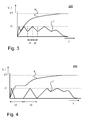
- first graph 300 depicted by Figure 3 Two possibly ways of operating the circuit 100 as depicted by Figure 1 will now be first discussed in conjunction with a first graph 300 depicted by Figure 3 and subsequently with a second graph 400 depicted by Figure 4 .
- Both the first graph 300 and the second graph 400 indicate time on the horizontal axis.
- the current through the inductor 106 and voltage between the first output terminal 126 and the second output terminal 128 are indicated.
- the first graph 300 indicates the previously mentioned voltage and current characteristics over time with a first switching scheme.
- the MOSFET 102 is switched on by the control circuit 150 until the current reaches a first pre-determined current value I1.
- the current level increases substantially linearly as the current also flows from the first input terminal to the first output terminal via the inductor 106.
- a current through an inductance cannot have a step function and in practice always increases in a continuous way.
- the first graph 300 and the second graph 400 are schematic visualisations of possible circuit characteristics and are not actual characteristics, either measured or simulated.
- the first pre-determined current value is in this embodiment determined by a maximum allowable current through the MOSFET 102.
- This maximum allowable current can be a specified continuous maximum current, a specified maximum peak current or another current level in relation to a projected MOSFET lifetime required for proper functionality of the circuit 100.
- the time for the current through the current sensor 104 to reach the first per-determined current value is measured and stored by the control circuit 105 as a first pre-determined time period t1. If the current through the current sensor 104 is detected to reach the first pre-determined current level I1, the MOSFET 102 is switched off. The MOSFET 102 is switched on again after the earlier measured and stored first pre-determined time period t1 has lapsed, which second pre-determined time period is indicated as t2 in the first graph 300.
- the second pre-determined time period t2 is a function of the first pre-determined time period t1.
- the function is preferably a multiplying function, where the first pre-determined time period t1 is multiplied with a factor between 0.5 and 1.5. In particular a factor of 1 is preferred.
- the MOSFET 102 is switched on again. Subsequently, the MOSFET 102 is switched off again as the current sensed by the current sensor 104 reaches the first pre-determined current level I1 again. During this on-state of the MOSFET 102, the first pre-determined time period t1 is measured again and the second pre-determined time period t2 is determined again. Following this on-state of the MOSFET 102, the MOSFET 102 is switched off again upon the current reaching the first pre-determined current level I1 for the second pre-determined time period t2.
- the voltage over the load 140 is measured during the charging process.
- V1 the voltage over the capacitance with gradually increase towards an asymptotic value that is the same as the voltage over the DC supply. This voltage is indicated in the first graph 300 as V1.
- the charging procedure ends.
- the pre-determined voltage level is preferably within a certain range of the voltage of the battery 130, for example 5% to 10% lower than the battery voltage.
- the third switch 152 is switched to a conductive state to connect the battery 130 directly to the load 140.
- a charged state of the capacitance 142 is detected by monitoring the current through the inductor 106 and/or through the MOSFET 102. In case the current through the MOSFET 102 while the MOSFET 102 is in on state (conductive state) does not reach a certain level during a pre-determined amount of time, the capacitance 142 is at least almost fully charged. This is also indicated in the first graph 300, where the current gradually drops as the voltage over the capacitance 142 is gradually approaching an asymptotic value indicated as V1.
- the second graph 400 indicates the previously mentioned voltage and current characteristics over time with a second switching scheme.
- the MOSFET 102 is switched on by the control circuit 150 until the current reaches a first pre-determined current value I1.
- the current level increases substantially linearly as the current also flows from the first input terminal to the first output terminal via the inductor 106.
- the pre-determined current value is in this embodiment determined by a maximum allowable current through the MOSFET 102.
- This maximum allowable current can be a specified continuous maximum current, a specified maximum peak current or another current level in relation to a projected MOSFET lifetime required for proper functionality of the circuit 100.
- the MOSFET 102 After the MOSFET 102 has been switched off, it is switched on again after a pre-determined period of time has lapsed since the previous time the MOSFET 102 has been switched on. This pre-determined amount of time is indicated with t3 at the horizontal axis of the second graph 400. This means that the period between the moment the MOSFET 102 is switched off and the moment the MOSFET 102 is switched on again is variable and depends on the rate with which the current through the MOSFET 102 reaches the pre-determined maximum level.
- the second graph 400 shows that during the largest part of the first period - indicated by t3 - no current flows through the inductor 106. As long as no current flows through the inductor 106, the capacitance 142 is not charged any further. This in turn means that the voltage over the capacitance 142 does not increase any further. As the capacitance 142 is further charged, the current rises less quickly and the MOSFET102 will be switched on for a longer part of the pre-determined period of t3.
- the moment that the capacitance 142 is sufficiently charged can be determined as discussed above, upon which moment the third switch 152 is switched to conductive state as well. At the moment the capacitance 142 is sufficiently charged by the battery 130 through the circuit 100, no too large currents will flow anymore from the battery 130 to the load 140 to charge the capacitance 142 as the voltage difference between both is relatively low or even negligible.
- the first switching scheme has a variable frequency with a duty cycle of 50% and the second switching scheme has a fixed frequency of 1/t3 and a variable duty cycle.
- the second switching scheme has a fixed frequency of 1/t3 and a variable duty cycle.
- the first switch 102 is preferably implemented by the MOSFET102.
- MOSFET102 solid state devices
- other solid state devices may be used, like an IGBT or other.
- the same or other semiconductor devices may be used for the second switch 154 and the third switch 152.
- relays may be used to implement the second switch 154 and the third switch 152.
- the battery 130 has a voltage of 360 V
- the required pre-charge time is 100 ms
- the capacitance 142 has a value of 1000uF.
- the average charging current is 3.6 A.
- the inductor may be comprised by the circuit 100 as disclosed by Figure 1 or may be provided separately, where the circuit 100 is provided without the inductor 106.
- the invention may also be embodied with less components than provided in the embodiments described here, wherein one component carries out multiple functions.
- the invention may also be embodied using more elements than depicted in Figure 1 , wherein functions carried out by one component in the embodiment provided are distributed over multiple components.
Landscapes
- Engineering & Computer Science (AREA)
- Power Engineering (AREA)
- Transportation (AREA)
- Mechanical Engineering (AREA)
- Charge And Discharge Circuits For Batteries Or The Like (AREA)
- Dc-Dc Converters (AREA)
Priority Applications (3)
| Application Number | Priority Date | Filing Date | Title |
|---|---|---|---|
| EP11181239A EP2570293A1 (fr) | 2011-09-14 | 2011-09-14 | Circuit de chargement et procédé de fonctionnement de ce circuit |
| US13/610,185 US9160192B2 (en) | 2011-09-14 | 2012-09-11 | Charging circuit with inductance-based current limiting and method for operating such circuit |
| CN201210337150.2A CN103001278B (zh) | 2011-09-14 | 2012-09-12 | 充电电路和用于操作该种充电电路的方法 |
Applications Claiming Priority (1)
| Application Number | Priority Date | Filing Date | Title |
|---|---|---|---|
| EP11181239A EP2570293A1 (fr) | 2011-09-14 | 2011-09-14 | Circuit de chargement et procédé de fonctionnement de ce circuit |
Publications (1)
| Publication Number | Publication Date |
|---|---|
| EP2570293A1 true EP2570293A1 (fr) | 2013-03-20 |
Family
ID=44763884
Family Applications (1)
| Application Number | Title | Priority Date | Filing Date |
|---|---|---|---|
| EP11181239A Withdrawn EP2570293A1 (fr) | 2011-09-14 | 2011-09-14 | Circuit de chargement et procédé de fonctionnement de ce circuit |
Country Status (3)
| Country | Link |
|---|---|
| US (1) | US9160192B2 (fr) |
| EP (1) | EP2570293A1 (fr) |
| CN (1) | CN103001278B (fr) |
Cited By (1)
| Publication number | Priority date | Publication date | Assignee | Title |
|---|---|---|---|---|
| US9797933B2 (en) | 2014-05-09 | 2017-10-24 | Dspace Digital Signal Processing And Control Engineering Gmbh | Method for monitoring the power consumption of an electrical consumer |
Families Citing this family (6)
| Publication number | Priority date | Publication date | Assignee | Title |
|---|---|---|---|---|
| US9925878B2 (en) | 2013-09-26 | 2018-03-27 | Ford Global Technologies, Llc | Bus pre-charge control using a buck converter |
| GB201514330D0 (en) * | 2015-08-12 | 2015-09-23 | Isis Innovation | Smart cells and control methods and systems |
| US11063465B2 (en) * | 2018-01-30 | 2021-07-13 | Novatel Inc. | Switching mode front end surge protection circuit |
| CN112810445A (zh) * | 2019-10-31 | 2021-05-18 | 宝马汽车股份有限公司 | 用于为车辆供电的电路和车辆 |
| CN110789368B (zh) * | 2019-11-12 | 2022-11-29 | 奇瑞汽车股份有限公司 | 电动汽车预充电路及其控制方法 |
| EP4236050A3 (fr) * | 2020-04-21 | 2023-11-29 | Go Electric, Inc. | Précharge adaptable |
Citations (7)
| Publication number | Priority date | Publication date | Assignee | Title |
|---|---|---|---|---|
| JPH10164709A (ja) * | 1996-11-27 | 1998-06-19 | Isuzu Motors Ltd | 電源装置および電気自動車用電源装置 |
| WO1999061965A1 (fr) * | 1998-05-27 | 1999-12-02 | Maxim Integrated Products, Inc. | Alimentations a decoupage avec mode de pseudo-elevation de tension, de pseudo-abaissement de tension et de precharge lineaire |
| US6208896B1 (en) * | 1998-11-13 | 2001-03-27 | Agilent Technologies, Inc. | Method and apparatus for providing variable defibrillation waveforms using switch-mode amplification |
| US20060071639A1 (en) * | 2004-09-30 | 2006-04-06 | Nanotechnologies, Inc. | Method and circuitry for charging a capacitor to provide a high pulsed power discharge |
| DE102004057690A1 (de) * | 2004-11-30 | 2006-06-01 | Robert Bosch Gmbh | Vorrichtung und Verfahren zum Laden einer elektrischen Energiespeichereinrichtung |
| US20070108959A1 (en) * | 2005-11-15 | 2007-05-17 | Toyota Jidosha Kabushiki Kaisha | Power supply control device and precharge processing method |
| US20100109617A1 (en) * | 2005-01-18 | 2010-05-06 | Puls Gmbh | Current-limiting circuit and method for operating the circuit |
Family Cites Families (2)
| Publication number | Priority date | Publication date | Assignee | Title |
|---|---|---|---|---|
| US6128323A (en) * | 1997-04-23 | 2000-10-03 | Cymer, Inc. | Reliable modular production quality narrow-band high REP rate excimer laser |
| US6677730B2 (en) * | 2001-12-21 | 2004-01-13 | Energenx, Inc. | Device and method for pulse charging a battery and for driving other devices with a pulse |
-
2011
- 2011-09-14 EP EP11181239A patent/EP2570293A1/fr not_active Withdrawn
-
2012
- 2012-09-11 US US13/610,185 patent/US9160192B2/en active Active
- 2012-09-12 CN CN201210337150.2A patent/CN103001278B/zh not_active Expired - Fee Related
Patent Citations (7)
| Publication number | Priority date | Publication date | Assignee | Title |
|---|---|---|---|---|
| JPH10164709A (ja) * | 1996-11-27 | 1998-06-19 | Isuzu Motors Ltd | 電源装置および電気自動車用電源装置 |
| WO1999061965A1 (fr) * | 1998-05-27 | 1999-12-02 | Maxim Integrated Products, Inc. | Alimentations a decoupage avec mode de pseudo-elevation de tension, de pseudo-abaissement de tension et de precharge lineaire |
| US6208896B1 (en) * | 1998-11-13 | 2001-03-27 | Agilent Technologies, Inc. | Method and apparatus for providing variable defibrillation waveforms using switch-mode amplification |
| US20060071639A1 (en) * | 2004-09-30 | 2006-04-06 | Nanotechnologies, Inc. | Method and circuitry for charging a capacitor to provide a high pulsed power discharge |
| DE102004057690A1 (de) * | 2004-11-30 | 2006-06-01 | Robert Bosch Gmbh | Vorrichtung und Verfahren zum Laden einer elektrischen Energiespeichereinrichtung |
| US20100109617A1 (en) * | 2005-01-18 | 2010-05-06 | Puls Gmbh | Current-limiting circuit and method for operating the circuit |
| US20070108959A1 (en) * | 2005-11-15 | 2007-05-17 | Toyota Jidosha Kabushiki Kaisha | Power supply control device and precharge processing method |
Cited By (1)
| Publication number | Priority date | Publication date | Assignee | Title |
|---|---|---|---|---|
| US9797933B2 (en) | 2014-05-09 | 2017-10-24 | Dspace Digital Signal Processing And Control Engineering Gmbh | Method for monitoring the power consumption of an electrical consumer |
Also Published As
| Publication number | Publication date |
|---|---|
| CN103001278A (zh) | 2013-03-27 |
| US20130063087A1 (en) | 2013-03-14 |
| CN103001278B (zh) | 2017-01-18 |
| US9160192B2 (en) | 2015-10-13 |
Similar Documents
| Publication | Publication Date | Title |
|---|---|---|
| US9160192B2 (en) | Charging circuit with inductance-based current limiting and method for operating such circuit | |
| CN109774465B (zh) | 可变电阻功率开关反馈 | |
| CN109168326B (zh) | 电源装置 | |
| CN102386799B (zh) | 电源电路及电力变换装置 | |
| CN106664021B (zh) | 控制高侧栅极驱动器的电源电压 | |
| US10046663B2 (en) | Electronic device for controlling the electric charge of a load electrically supplied by a battery pack and system for moving an electric or hybrid traction vehicle using the device | |
| US20130234510A1 (en) | Electric vehicle inverter device | |
| CN108134511B (zh) | 利用温度补偿的截止的栅极驱动器 | |
| EP2113995A1 (fr) | Dispositif de source d'energie electrique | |
| CN105580233B (zh) | 功率转换装置 | |
| CN108432114A (zh) | 使用具有旁路模式的电力转换器进行无线电力传输的系统和方法 | |
| CN105706366B (zh) | 栅极驱动电路以及使用该栅极驱动电路的电力变换装置 | |
| CN104917220B (zh) | 切换电路及电机能源回收系统 | |
| CN107222091A (zh) | 用于降低开关损耗的动态igbt栅极驱动 | |
| CN103036457B (zh) | 交流直流转换器 | |
| JP2019527027A (ja) | 電流コンバータの駆動方法およびその方法で駆動される電流コンバータ | |
| CN105896940A (zh) | 电力转换装置 | |
| CN107000600B (zh) | 用于通过逆变器给电池单元充电并且运行负载单元的装置 | |
| KR101948976B1 (ko) | 인버터 제어 회로 | |
| JP2016119759A (ja) | 非接触給電システム及び送電装置 | |
| CN103201132B (zh) | 车辆用辅助电源装置 | |
| JP2017192183A (ja) | Dc−dc電圧変換装置 | |
| JP5715363B2 (ja) | 誘導性負荷駆動装置 | |
| CN114514681A (zh) | Dcdc转换器 | |
| KR102345532B1 (ko) | 전압 감지 장치 |
Legal Events
| Date | Code | Title | Description |
|---|---|---|---|
| PUAI | Public reference made under article 153(3) epc to a published international application that has entered the european phase |
Free format text: ORIGINAL CODE: 0009012 |
|
| AK | Designated contracting states |
Kind code of ref document: A1 Designated state(s): AL AT BE BG CH CY CZ DE DK EE ES FI FR GB GR HR HU IE IS IT LI LT LU LV MC MK MT NL NO PL PT RO RS SE SI SK SM TR |
|
| AX | Request for extension of the european patent |
Extension state: BA ME |
|
| 17P | Request for examination filed |
Effective date: 20130920 |
|
| RBV | Designated contracting states (corrected) |
Designated state(s): AL AT BE BG CH CY CZ DE DK EE ES FI FR GB GR HR HU IE IS IT LI LT LU LV MC MK MT NL NO PL PT RO RS SE SI SK SM TR |
|
| STAA | Information on the status of an ep patent application or granted ep patent |
Free format text: STATUS: EXAMINATION IS IN PROGRESS |
|
| 17Q | First examination report despatched |
Effective date: 20180410 |
|
| STAA | Information on the status of an ep patent application or granted ep patent |
Free format text: STATUS: THE APPLICATION IS DEEMED TO BE WITHDRAWN |
|
| 18D | Application deemed to be withdrawn |
Effective date: 20180821 |