EP2570854A1 - Bestimmung der Form der Beleuchtungsquelle in optischer Lithographie - Google Patents
Bestimmung der Form der Beleuchtungsquelle in optischer Lithographie Download PDFInfo
- Publication number
- EP2570854A1 EP2570854A1 EP11181654A EP11181654A EP2570854A1 EP 2570854 A1 EP2570854 A1 EP 2570854A1 EP 11181654 A EP11181654 A EP 11181654A EP 11181654 A EP11181654 A EP 11181654A EP 2570854 A1 EP2570854 A1 EP 2570854A1
- Authority
- EP
- European Patent Office
- Prior art keywords
- mask
- optimization
- mask design
- illumination source
- lithographic
- Prior art date
- Legal status (The legal status is an assumption and is not a legal conclusion. Google has not performed a legal analysis and makes no representation as to the accuracy of the status listed.)
- Granted
Links
Images


Classifications
-
- G—PHYSICS
- G03—PHOTOGRAPHY; CINEMATOGRAPHY; ANALOGOUS TECHNIQUES USING WAVES OTHER THAN OPTICAL WAVES; ELECTROGRAPHY; HOLOGRAPHY
- G03F—PHOTOMECHANICAL PRODUCTION OF TEXTURED OR PATTERNED SURFACES, e.g. FOR PRINTING, FOR PROCESSING OF SEMICONDUCTOR DEVICES; MATERIALS THEREFOR; ORIGINALS THEREFOR; APPARATUS SPECIALLY ADAPTED THEREFOR
- G03F7/00—Photomechanical, e.g. photolithographic, production of textured or patterned surfaces, e.g. printing surfaces; Materials therefor, e.g. comprising photoresists; Apparatus specially adapted therefor
- G03F7/70—Microphotolithographic exposure; Apparatus therefor
- G03F7/70058—Mask illumination systems
- G03F7/70125—Use of illumination settings tailored to particular mask patterns
-
- G—PHYSICS
- G03—PHOTOGRAPHY; CINEMATOGRAPHY; ANALOGOUS TECHNIQUES USING WAVES OTHER THAN OPTICAL WAVES; ELECTROGRAPHY; HOLOGRAPHY
- G03F—PHOTOMECHANICAL PRODUCTION OF TEXTURED OR PATTERNED SURFACES, e.g. FOR PRINTING, FOR PROCESSING OF SEMICONDUCTOR DEVICES; MATERIALS THEREFOR; ORIGINALS THEREFOR; APPARATUS SPECIALLY ADAPTED THEREFOR
- G03F1/00—Originals for photomechanical production of textured or patterned surfaces, e.g., masks, photo-masks, reticles; Mask blanks or pellicles therefor; Containers specially adapted therefor; Preparation thereof
- G03F1/36—Masks having proximity correction features; Preparation thereof, e.g. optical proximity correction [OPC] design processes
-
- G—PHYSICS
- G03—PHOTOGRAPHY; CINEMATOGRAPHY; ANALOGOUS TECHNIQUES USING WAVES OTHER THAN OPTICAL WAVES; ELECTROGRAPHY; HOLOGRAPHY
- G03F—PHOTOMECHANICAL PRODUCTION OF TEXTURED OR PATTERNED SURFACES, e.g. FOR PRINTING, FOR PROCESSING OF SEMICONDUCTOR DEVICES; MATERIALS THEREFOR; ORIGINALS THEREFOR; APPARATUS SPECIALLY ADAPTED THEREFOR
- G03F7/00—Photomechanical, e.g. photolithographic, production of textured or patterned surfaces, e.g. printing surfaces; Materials therefor, e.g. comprising photoresists; Apparatus specially adapted therefor
- G03F7/70—Microphotolithographic exposure; Apparatus therefor
- G03F7/70425—Imaging strategies, e.g. for increasing throughput or resolution, printing product fields larger than the image field or compensating lithography- or non-lithography errors, e.g. proximity correction, mix-and-match, stitching or double patterning
-
- G—PHYSICS
- G03—PHOTOGRAPHY; CINEMATOGRAPHY; ANALOGOUS TECHNIQUES USING WAVES OTHER THAN OPTICAL WAVES; ELECTROGRAPHY; HOLOGRAPHY
- G03F—PHOTOMECHANICAL PRODUCTION OF TEXTURED OR PATTERNED SURFACES, e.g. FOR PRINTING, FOR PROCESSING OF SEMICONDUCTOR DEVICES; MATERIALS THEREFOR; ORIGINALS THEREFOR; APPARATUS SPECIALLY ADAPTED THEREFOR
- G03F7/00—Photomechanical, e.g. photolithographic, production of textured or patterned surfaces, e.g. printing surfaces; Materials therefor, e.g. comprising photoresists; Apparatus specially adapted therefor
- G03F7/70—Microphotolithographic exposure; Apparatus therefor
- G03F7/70425—Imaging strategies, e.g. for increasing throughput or resolution, printing product fields larger than the image field or compensating lithography- or non-lithography errors, e.g. proximity correction, mix-and-match, stitching or double patterning
- G03F7/70433—Layout for increasing efficiency or for compensating imaging errors, e.g. layout of exposure fields for reducing focus errors; Use of mask features for increasing efficiency or for compensating imaging errors
-
- G—PHYSICS
- G03—PHOTOGRAPHY; CINEMATOGRAPHY; ANALOGOUS TECHNIQUES USING WAVES OTHER THAN OPTICAL WAVES; ELECTROGRAPHY; HOLOGRAPHY
- G03F—PHOTOMECHANICAL PRODUCTION OF TEXTURED OR PATTERNED SURFACES, e.g. FOR PRINTING, FOR PROCESSING OF SEMICONDUCTOR DEVICES; MATERIALS THEREFOR; ORIGINALS THEREFOR; APPARATUS SPECIALLY ADAPTED THEREFOR
- G03F7/00—Photomechanical, e.g. photolithographic, production of textured or patterned surfaces, e.g. printing surfaces; Materials therefor, e.g. comprising photoresists; Apparatus specially adapted therefor
- G03F7/70—Microphotolithographic exposure; Apparatus therefor
- G03F7/70425—Imaging strategies, e.g. for increasing throughput or resolution, printing product fields larger than the image field or compensating lithography- or non-lithography errors, e.g. proximity correction, mix-and-match, stitching or double patterning
- G03F7/70433—Layout for increasing efficiency or for compensating imaging errors, e.g. layout of exposure fields for reducing focus errors; Use of mask features for increasing efficiency or for compensating imaging errors
- G03F7/70441—Optical proximity correction [OPC]
Definitions
- the invention relates to the field of optical lithography. More specifically it relates to methods and systems for optimizing lithographic processing such as optimizing source illumination, threshold and mask to be used for lithographic processing.
- Optical lithography is one of the technologies that are being used in the production of microchips. It uses a 'reticle', also called 'photomask' or 'mask' to form certain patterns in a 'photo-resist layer' that is coated on a 'wafer'.
- This mask contains a pattern that, when an image of it is projected on the wafer, generates the desired pattern in this photoresist layer, after it has been chemically developed.
- This projected image is formed on the photoresist layer by illuminating the mask with a certain wavelength and light-source shape. The light passing through the mask is then captured by the projection lens of the lithography exposure tool, and this lens forms an image of the mask pattern in the photoresist layer.
- the mask itself consists of an optically-transparent plate on which patterns have been created at one side: these patterns consist of polygons in which the optical-transmission properties of the mask are modified with respect to the 'unpatterned areas'.
- these polygon-shaped mask patterns might consist of a thin layer that absorbs or attenuated the light that passes through them.
- optical-projection-lithography is however complicated by two elements.
- the shapes in the image that is formed on the wafer is never an identical copy of the shape of the patterns on the mask, and the difference between the two has become larger as the 'technology node' for which the lithography step is being used becomes more advanced, that is, as the pattern size and pattern density that need to be generated are becoming respectively smaller and denser such as for example below the 20nm node.
- This effect of the difference between mask- and projected-image-pattern is called the 'optical proximity effect'.
- the mask pattern is intentionally made different from the image that one wants to form on the wafer, but in such a way that its projected image becomes closer to the desired wafer pattern.
- This modification in general implies that the shape of the mask patterns (polygons) is made different from the desired printed shapes in some appropriate way, but it can also imply adding additional polygons to the mask pattern that are not supposed to form printing images on the wafer but somehow improve the process latitudes (see next bullet) of the polygons that are supposed to print.
- These 'extra' mask polygons are often called 'assist mask features', or 'assist features'.
- OPC has been a standard technology for many years now, and several companies offer software that generates the optical proximity corrected mask pattern, if the intended wafer pattern is given, together with enough details on the way the mask will be exposed in the lithography tool.
- the second element that makes optical-projection-lithography more complicated is that the fidelity of the wafer pattern is also affected by the presence of (to a certain extent unavoidable) imperfections in the lithographic process, a number of them being listed here.
- the printed pattern shape depends on the amount of light that is being used to generated the images on the wafer, the so-called 'exposure dose' or 'dose'.
- lithographers aim to work under conditions where they have a sufficient amount of 'exposure latitude (EL)', that is conditions under which a certain offset from the ideal dose (usually expressed as a percentage of the dose itself) can be tolerated.
- EL 'exposure latitude
- the lithographic projection lens forming the image has a so-called 'best-focus plane', i.e. a certain plane in space where the image is most 'sharp' and hence closest to the intended image. If the wafer is not ideally located with respect to this best-focus plane, one says that the wafer is 'out-of-focus'.
- lithographers aim to work under conditions where they have a sufficient amount of 'depth-of-focus (DOF)', that is conditions under which a certain offset from the ideal focus plane (usually expressed by saying how many nanometer the actual wafer plane is away from the ideal plane) can be tolerated.
- DOE 'depth-of-focus
- the mask patterns as generated by e.g the above mentioned OPC-software can in general not be perfectly realized on the actual photo-mask that is being used in the lithographic process: usually there are 'mask errors', i.e. the mask patterns deviate either in size or shape (or both) from the desired mask pattern.
- any deviation from the desired mask pattern also leads to a deviation of the wafer pattern.
- lithographers aim to work in conditions under which some amount of mask error can be tolerated.
- lithographic-process conditions under which enough EL, DOF and tolerance against mask errors is realized.
- the actual performance of a lithographic process with respect to the mentioned tolerances is often quantified in a metric that is called the 'critical dimension uniformity', abbreviated as CDU (expressed in nanometer). This metric expresses how much the dimension of a certain structure in the wafer image will actually vary (e.g.
- 'SMO' source-mask optimization
- This is a computational process in which the illumination source and the OPCed mask are varied simultaneously in order to find the source-mask combination that offers the best possible or at least sufficient tolerances (also called 'process margins') for dose, focus and/or mask error.
- Several software companies offer automated software to do such an SMO calculation, if the desired wafer image is given, together with other inputs such as the desired process margins and certain parameters that define limitations on the mask complexity that is allowed by the user.
- both OPC- and SMO-software have a number of numerical parameters that influence (limit) the complexity of the solution that the user is willing to accept, and for which the user of the software has to choose numerical value or settings he thinks are appropriate.
- the actual complexity of the assist polygons that appear in the final mask solution is further influenced by the values of a set of input parameters for the SMO calculation that are called 'mask-rule check' or MRC parameters.
- the actual values for these parameters (that have to be set by the person who runs the calculation) set limits to the allowed complexity of each individual mask polygon.
- these MRC parameters set minimum values to the allowed segment length of mask polygons.
- An MRC parameter set that allows very complex shapes would be called 'aggressive': the printed image shape with such an aggressive set of MRC input parameters would in general be closer to the desired ideal image, but the resulting mask might be non-manufacturable or very expensive. This is why in general people prefer to run SMO software with more 'moderate MRC' input parameters, leading to a less perfect printed image but outputting a less complex and hence more manufacturable or less expensive mask.
- lithographic processing conditions can be determined for providing a lithographic process with a good depth of focus (DoF) performance while allowing low complexity of sub-resolution assist features in the mask used. It is an advantage of embodiments of the present invention that the manufacturing effort and economical cost for manufacturing masks can be low, while still obtaining a lithographic process with a good DoF performance.
- DoF depth of focus
- lithographic processing conditions can be determined for a lithographic process wherein the mask complexity is low or limited (i.e. for example only rectangular shaped sub-resolution assist features being presence), while the lithographic process allows obtaining a similar or the same critical dimension uniformity (CDU) as would be the case if also non-rectangular shaped sub-resolution features would have be allowed in the mask.
- CDU critical dimension uniformity
- the size of the mask file, defining the mask features and the sub-resolution assist features used can be limited, while still obtaining good lithographic processing.
- the present invention relates to a method for determining lithographic processing conditions for a lithographic process, the method comprising obtaining characteristics of an illumination source and a mask design, the mask design comprising a lithography pattern, performing a first optimization for combined optimizing of the illumination source characteristics and the mask design characteristics for the lithographic process, whereby for said first optimization non-rectangular sub-resolution assist features for the mask are allowed, determining from said first optimization a set of optimized illumination source characteristics, performing one or more further optimizations for optimizing the mask design characteristics of the lithographic process, whereby for said one or more further optimizations the presence of non-rectangular sub-resolution assist features for said mask design is substantially excluded and whereby said one or more further optimizations takes into account said set of optimized illumination source characteristics, and determining from said one or more further optimizations a set of optimized mask design characteristics substantially excluding non-rectangular sub-resolution assist features.
- the one or more further optimizations may be performed taking into account mask rule check settings expressing at least that the most complex mask design feature allowed in the one or more further optimizations is less complex than the most complex mask design feature allowed in the first optimization. It is an advantage of at least some embodiments of the present invention that not only the sub-resolution assist features may be less complex in the final mask design but also the other mask features may be less complex in the final mask design, compared to mask features in a mask design made using conventional mask optimization for good lithographic processing.
- the first optimization may be performed on an optimization clip, being only a part of the mask design. It is an advantage of at least some embodiments of the present invention that optimization can be performed on only a small part of the mask, thus allowing efficient processing with limited computing power.
- the one or more optimizations may comprise optimizing a threshold for the lithographic processing.
- Performing the one or more optimizations may comprise performing a second optimization for optimizing of the threshold and the mask design characteristics of the lithographic process, whereby for said second optimization the presence of non-rectangular sub-resolution assist features for said mask is substantially excluded and whereby the second optimization takes into account the set of optimized illumination source characteristics, and performing a third optimization for optimizing the mask design characteristics for the lithographic process, whereby for the third optimization the presence of non-rectangular sub-resolution assist features for said mask is substantially excluded and whereby the third optimization takes into account the set of optimized illumination source characteristics determined from the first optimization and an optimized threshold determined from the second optimization.
- the illumination source, the threshold and the mask characteristics to be selected can be optimized in different optimization steps, allowing to optimize each parameter with its own assist- and mask rule check settings. It is an advantage of at least some embodiments that the use of different assist- and mask rule check settings can allow to optimize the illumination source, the threshold and the mask characteristics such that a good DoF and/or CDU can be obtained using the lithographic processing and simultaneously a mask with limited complexity can be used for lithographic processing.
- Performing he second optimization may be applied for an optimization clip, being only a part of the mask design. It is an advantage of at least some embodiments of the present invention that optimization can be performed on only a small part of the mask, thus allowing efficient processing with limited computing power.
- Performing the third optimization may be applied for the full mask design. It is an advantage of at least some embodiments of the present invention that mask features can be determined for the full mask can be obtained.
- the lithographic process may comprise multiple patterning steps for patterning different portions of a pattern to be processed.
- Embodiments of the present invention may be especially suitable for multiple patterning lithographic processing as in multiple patterning as the sub-patterns typically have a wide spacing between the features. In other words, using multiple patterning lithographic processing, there is more frequent occurrence of isolated patterns. As this has intrinsically negative impact on the depth of focus margin and the CD (critical dimension) variation, strategies for improving depth of focus and CD uniformity as obtained with at least some embodiments of the present invention are beneficial for the multiple patterning technique.
- a source-mask optimization algorithm may be used based on any of a full resist model or an aerial image model.
- the present invention also relates to a system for determining lithographic processing conditions for a lithographic process, the system comprising an input means for obtaining characteristics of an illumination source and a mask design, the mask design comprising a lithography pattern and sub-resolution assist features, a processing means programmed for performing a first optimization for combined optimizing of the illumination source characteristics and the mask design characteristics for the lithographic process, whereby for said first optimization non-rectangular sub-resolution assist features for the mask are allowed, determining from said first optimization a set of optimized illumination source characteristics, performing one or more further optimizations for optimizing the mask design characteristics of the lithographic process, whereby for said one or more further optimizations the presence of non-rectangular sub-resolution assist features for said mask is substantially excluded and whereby said one or more further optimizations takes into account said set of optimized illumination source characteristics, and determining from said one or more further optimizations a set of optimized mask design characteristics substantially excluding non-rectangular sub-resolution assist features.
- the processing means may be adapted for performing a second optimization for optimizing of the threshold and the mask design characteristics of the lithographic process, whereby for said second optimization the presence of non-rectangular sub-resolution assist features for said mask is substantially excluded and whereby the second optimization takes into account the set of optimized illumination source characteristics, and a third optimization for optimizing the mask design characteristics for the lithographic process, whereby for the third optimization the presence of non-rectangular sub-resolution assist features for said mask is substantially excluded and whereby the third optimization takes into account the set of optimized illumination source characteristics determined from the first optimization and an optimized threshold determined from the second optimization.
- the system may be implemented as a computer program product for, when executing on a processing means, carrying out one of the methods as described above.
- the present invention also relates to a data carrier for storing a computer program product for, when executing on a processing means, carrying out one of the methods as described above.
- the present invention also relates to the transmission of a computer program product for, when executing on a processing means, carrying out one of the methods as described above.
- the present invention furthermore relates to a kit of parts for use in lithographic processing, the kit of parts comprising a carrier comprising illumination source characteristics determined using a method as described above, and a mask according to a mask design determined using the same method.
- the present invention furthermore relates to an electronic device, the electronic device comprising at least one patterned layer, the patterned layer being made using lithographic processing according to lithographic processing conditions determined using a method as described above.
- the present invention also relates to a method of manufacturing an electronic device, the method comprising determining a set of lithographic processing conditions comprising illumination source characteristics and mask characteristics using a method for determining lithographic processing conditions as described above, and exposing a photoresist layer on a semiconductor substrate using the lithographic processing conditions for forming the electronic device.
- SRAF sub-resolution assist features
- a first type are the rectangular sub-resolution assist features which are generally rectangular in shape.
- a second type are non-rectangular sub-resolution assist features (SRAF) which comprise, besides optionally rectangular features, also non-rectangular shaped SRAF portions. These are also referred to as free-from SRAF.
- assist features can be objects of any shape, for example polygons with an arbitrary high number of vertex points.
- non-rectangular SRAF may be limited to polygonal shaped SRAF and even to polygonal shaped SRAF wherein the angles used are limited to 0°, 90°, 180° or 270°, embodiments of the present invention not being limited thereby.
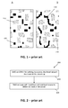
- FIG. 1 an illustration of rectangular SRAF correction (part A) and non-rectangular SRAF (part B) correction for double patterning is shown in FIG. 1 .
- the black portions indicate the sub-resolution assist features whereas the hatched portions indicate the original pattern features.
- the use of non-rectangular SRAF in double patterning substantially increases the depth of focus (DoF), but also substantially increases the mask file size (GDS).
- SMO source-mask optimization
- the optimization may have different effects on different edges and features of the irradiation source. It may for example have an effect on the source shape or the irradiation pattern. It may for example also include the use of pupils to restrict the source illumination to a selected pattern of radiation.
- Optimizing the mask may have an effect on different features and edges of the mask. It may for example include shifting or biasing edge positions or line widths as well as application of assist features that are not intended to print themselves but will affect the properties of an associated pattern feature to be printed.
- the SMO typically also includes optimization of the threshold.
- the threshold reference is made to the irradiation intensity or dose used for irradiating and above which the irradiated photoresist will be altered so that it can lead to formation of a pattern.
- the threshold used directly influences the critical dimension that can be obtained.
- FIG. 2 essential parts of such a conventional SMO flow 200 are shown.
- source mask optimization is implemented on a circuit clip, e.g. an SRAM cell, so as to define the source and the mask shape.
- the pattern used in this step is not necessary limited to one circuit clip such as an SRAM cell, but other clips e.g. from a logic circuit block or a combination thereof also can be used.
- mask optimization is performed on logic pattern, this part being essentially corresponding with the optical proximity correction (OPC).
- the SMO and MO optimization is performed under moderate mask restriction rules (MRC) and using rectangular SRAF, as for non-rectangular SRAF the GDS mask file size typically becomes very large. If a large GDS file size and a complex mask are not too restrictive, the conventional SMO flow also may be performed with more aggressive mask restriction rules and with non-rectangular SRAF.
- MRC moderate mask restriction rules
- rectangular SRAF rectangular SRAF
- the present invention relates to a method for determining lithographic processing conditions for a lithographic process.
- the method is especially suitable for patterning of small patterns.
- the method may be advantageously be used in multiple patterning processing, such as for example in double patterning lithographic processing, although embodiments of the present invention are not limited thereto.
- It makes use of an algorithm for source-mask optimization (SMO).
- SMO source-mask optimization
- Different algorithms for performing SMO are known in the art, and embodiments of the present invention can make use of each of such algorithm.
- An example of a SMO algorithm that can be used is described in international patent application WO2010/059954 A2 , although embodiments of the present invention are not limited thereto.
- Algorithms for source mask optimization typically may make use of optical imaging model simulations.
- the SMO optimization may make use of an aerial image model or a full resist model, embodiments of the present invention not being limited by the particular model used.
- embodiments of the present invention make use of different optimization steps.
- the same or a different SMO algorithm may be used, making use of the same or a different optical imaging simulation model such as an aerial image model or a full resist model.
- the source conditions are fixed, e.g. determined in a previous step.
- the algorithm also may be referred to as a mask optimization algorithm (MO).
- the method according to embodiments of the present invention comprises a step of obtaining characteristics of an illumination source and a mask design to be optimized.
- the mask design characteristics or mask design thereby comprise an initial pattern.
- the mask design characteristics may also comprise a set of sub-resolution assist features to be refined or these may be introduced during the optimization steps to be performed.
- a first optimization is performed for combined optimizing of the illumination source characteristics and the mask design characteristics for the lithographic process. According to embodiments of the present invention, this first optimization is performed such that non-rectangular sub-resolution assist features for the mask are allowed.
- a typical SMO algorithm may be used for this optimization, embodiments of the present invention not being limited thereto.
- the optimization may be based on a full resist model as well as on an aerial image model.
- the first optimization typically may be performed on an optimization clip, being only part of the mask design to be optimized, although embodiments of the present invention are not limited thereto. From this first optimization, a set of optimized illumination source characteristics as well as a set of optimized mask design characteristics is determined, but only the set of optimized illumination source characteristics is maintained and will be used further in the method.
- a step of performing one or more further optimizations is performed, for optimizing the mask design characteristics of the lithographic process.
- This optimization may be performed in a single step or in different optimizations, e.g. if other parameters such as for example the threshold also are to be optimised.
- the set of optimized illumination source characteristics as determined in the first optimization are used as fixed illumination source characteristics, without allowing further variation of these illumination source characteristics.
- the algorithm used may be the same or a different algorithm as used in the first optimization. It may be an algorithm based on a full resist model as well as an algorithm based on an aerial image model.
- the presence of non-rectangular sub-resolution assist features for the mask design is substantially excluded.
- the mask rule check settings may be set, such that less complex mask design features are allowed. These optimizations will result in a less complex mask design than obtained with the first optimization but surprisingly has the advantage of obtaining the good depth of focus (DoF) as would have been obtained when performing the optimization of illumination source and mask with non-rectangular sub-resolution assist features allowed.
- DoF good depth of focus
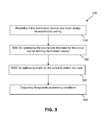
- FIG. 3 an exemplary method according to an embodiment of the present invention is illustrated in FIG. 3 .
- the exemplary method comprises obtaining 310 initial settings for the illumination source and the mask design.
- the separation between the optimization step for defining the source 320 and for defining the threshold and the mask 330 allows to use different conditions on the sub-resolution assist features, i.e. allows to define the source using mask characteristics allowing non-rectangular sub-resolution assist features and allows to define the mask characteristics and threshold using conditions not allowing non-rectangular sub-resolution assist features.
- the method also may comprise outputting 340 the lithographic processing conditions as determined above via an output port, to a data carrier, by displaying or in any other means.
- the output provided are lithographic processing conditions comprising information regarding the illuminations source to be used during lithographic processing as well as a mask design for use in the lithographic processing.
- Methods according to embodiments of the present invention advantageously are at least partially computer-implemented. For example, at least the optimization steps wherein the optimization algorithms are applied may be performed in a computer-implemented manner. In some embodiments, the method may be fully computer implemented.
- the one or more further optimizations also include optimization of the threshold for lithographic processing.
- the latter can be performed in a separate step or combined with the optimization step for the mask characteristics.
- optimization of the threshold and the mask design characteristics is performed in a single optimization step, following the optimization step for defining the illumination source characteristics.
- the latter then typically may be performed on the full mask design, i.e. for the full circuit, in order to obtain optimization of the full mask design.
- the threshold and the mask design characteristics are defined in the same step. According to embodiments of the present invention, this is performed while excluding non-rectangular sub-resolution assist features.
- optimization of the threshold and the mask design is performed in separate optimization steps.
- the one or more optimization steps may therefore comprise a second optimization step for optimizing the threshold and the mask design excluding non-rectangular sub-resolution assist features and using the illumination source settings defined in the first optimization.
- From the second optimization step at least the threshold setting is defined.
- part of the mask design characteristics e.g. those characteristics as obtained for a circuit clip being only part of the circuit mask design can be defined.
- the defined threshold and optionally also part of the mask design characteristics may then be used as fixed values for a third optimization step, wherein the mask design characteristics of the further mask design characteristics are determined for the full mask design, i.e. corresponding with the full circuit.
- mask rule check settings are parameters that set limits to the allowed complexity of each individual mask polygon.
- these MRC parameters may set minimum values to the allowed segment length of mask polygons.
- An MRC parameter set that allows very complex shapes would be called 'aggressive': the printed image shape with such an aggressive set of MRC input parameters would in general be closer to the desired ideal image, but the resulting mask is more complex and might be difficult to manufacture and/or very expensive.
- the mask rule check settings may be selected such that at least the most complex mask design feature allowed in the one or more further optimizations is less complex than the most complex mask design feature allowed in the first optimization. It is an advantage of embodiments according to the present invention that the threshold setting can be determined under the conditions wherein non-rectangular sub-resolution assist features are excluded, as this allows to have a good DoF, better than the one obtained using a conventional SMO flow wherein non-rectangular sub-resolution assist features are excluded.
- the different optimizations steps may be performed using SMO optimization algorithms based on the same or on different simulation models, e.g. using an aerial image model or a full resist model.
- FIG. 4 illustrates examples of SRAM patterns generated using a conventional flow with only rectangular SRAF allowed (flow A), using a conventional flow with non-rectangular SRAF allowed (flow B) and using an SMO flow according to an embodiment of the present invention (flow C). It can be seen that for the SMO flow according to an embodiment of the present invention, the number of SRAF is substantially larger than in flow A and that the layout of the SRAF is substantially more close to the conventional flow allowing non-rectangular SRAF (flow B). Comparison of the NILS for the conventional flow with only rectangular SRAF and for the flow according to an embodiment of the present invention indicates that there is a clear advantage on the NILS both for best focus and defocused conditions, as can be derived from FIG. 5.
- FIG. 5 illustrates the normalized image log slope (NILS) on the cut line indicated in FIG. 4 .
- FIG. 6 By way of illustration the major steps of a plurality of possible SMO flows are illustrated in FIG. 6 , illustrating some examples of different possible flows according to embodiments of the present invention.
- the present invention also relates to a system for determining lithographic processing conditions for a lithographic process.
- the system may be especially suitable for performing a method according to the first aspect as described above, although embodiments are not limited thereto.
- the system may be computer implemented. Such a computer-implementation may be software implemented as well as hardware implemented or a combination thereof.
- FIG. 7 an exemplary system according to an embodiment of the present invention is shown in FIG. 7 , illustrating standard and optional features of such a system.
- the system 700 comprises an input means 710 for obtaining characteristics of an illumination source and a mask design. The characteristics typically comprise a lithography pattern to be implemented.
- Sub resolution assist features may also already be defined for further optimization, or these may be introduced while optimizing, then not being part of the mask design characteristics.
- the input typically is obtained in electronic data format.
- the system furthermore comprises a processing means.
- the processing means 720 thereby is programmed for performing a first optimization for combined optimizing of the illumination source characteristics and the mask design characteristics for the lithographic process.
- the processing means 720 furthermore is programmed for performing the first optimization such that non-rectangular sub-resolution assist features for the mask are allowed.
- the processing means 720 also is programmed for determining from the first optimization a set of optimized illumination source characteristics.
- the processing means 720 also is programmed for performing one or more further optimizations for optimizing of the mask design characteristics of the lithographic process, whereby for the one or more further optimizations the presence of non-rectangular sub-resolution assist features for said mask is substantially excluded.
- the one or more further optimizations thereby take into account said set of optimized illumination source characteristics.
- the processing means 720 also is programmed for determining from the one or more further optimizations, a set of optimized mask design characteristics substantially excluding non-rectangular sub-resolution assist features.
- the processing means 720 furthermore may be adapted for taking into account different mask rule check settings for the different optimization steps.
- the processing means 720 may comprise a controller 722 for timing the different actions. Furthermore, the processing means 720 also may comprise a SMO optimization module 724, which is adapted for performing SMO optimization taking into account particular settings provided, e.g. particular settings provided for particular simulations. These particular settings may be obtained from user-input or may be obtained from the controller 722. Such settings may be settings determining the degree of complexity of the mask, settings determining whether or not non-rectangular assist features are accepted, mask rule check settings expressing a degree of complexity allowed for the pattern features, etc.
- the SMO optimization module 724 may be any suitable source mask optimization module known to the person skilled in the art.
- the system furthermore comprises an output means for putting out the lithographic processing conditions to be used.
- lithographic processing conditions typically comprise illumination source characteristics and mask design characteristics and can be outputted as electronic data, displayed, etc.
- Further system components may be any component adapted for performing one, more or part of steps of the method for determining lithographic processing conditions as described in the first aspect.
- the present invention relates to a computer program product for, when executing on a processing means, carrying out one of the methods as described in the first aspect.
- the computer program product may be implemented on a processing system that includes at least one programmable processor coupled to a memory subsystem that includes at least one form of memory, e.g., RAM, ROM, and so forth.
- the processor or processors may be a general purpose, or a special purpose processor, and may be for inclusion in a device, e.g., a chip that has other components that perform other functions.
- one or more aspects of embodiments of the present invention can be implemented in digital electronic circuitry, or in computer hardware, firmware, software, or in combinations of them.
- the processor may be adapted for performing a method for determining lithographic processing conditions or may comprise instructions for performing such a method.
- the processor may include a storage subsystem that has at least one disk drive and/or CD-ROM drive and/or DVD drive.
- a display system, a keyboard, and a pointing device may be included as part of a user interface subsystem to provide for a user to manually input information. Ports for inputting and outputting data also may be included. More elements such as network connections, interfaces to various devices, and so forth, may be included.
- the various elements of the processing system may be coupled in various ways, including via a bus subsystem.
- the memory of the memory subsystem may at some time hold part or all of a set of instructions that when executed on the processing system implement the steps of the method embodiments described above. While a processing system as such is prior art, a system that includes the instructions to implement aspects of the methods as described above is not prior art.
- the computer program product can be tangibly embodied in a carrier medium carrying machine-readable code for execution by a programmable processor.
- the present invention thus relates to a carrier medium carrying a computer program product that, when executed on computing means, provides instructions for executing determination of lithographic processing conditions according to any of the methods as described above.
- carrier medium refers to any medium that participates in providing instructions to a processor for execution. Such a medium may take many forms, including but not limited to, non-volatile media, and transmission media.
- Non-volatile media includes, for example, optical or magnetic disks, such as a storage device that is part of mass storage.
- Computer readable media include, a CD-ROM, a DVD, a flexible disk or floppy disk, a tape, a memory chip or cartridge or any other medium from which a computer can read.
- Various forms of computer readable media may be involved in carrying one or more sequences of one or more instructions to a processor for execution.
- the computer program product can also be transmitted via a carrier wave in a network, such as a LAN, a WAN or the Internet.
- Transmission media can take the form of acoustic or light waves, such as those generated during radio wave and infrared data communications. Transmission media include coaxial cables, copper wire and fibre optics, including the wires that comprise a bus within a computer.
- the present invention also relates to a kit of parts for use in lithographic processing.
- the kit of parts comprises a carrier comprising data including illumination source characteristics determined using a method as described in the first aspect, as well as a mask according to a mask design determined using the same method.
- the present invention also relates to an electronic device, wherein the electronic device comprises at least one patterned layer, the patterned layer being made using lithographic processing according to lithographic processing conditions determined using a method as described in the first aspect.
- the present invention relates to a method for manufacturing an electronic device, the method comprising determining a set of lithographic processing conditions using a method as described in the first aspect and thereafter exposing a photoresist on a semiconductor substrate using the lithographic processing conditions for forming an electronic device.
- the method may comprise obtaining characteristics of an illumination source and a mask design, the mask design comprising a lithography pattern and sub-resolution assist features, performing a first optimization for combined optimizing of the illumination source characteristics and the mask design characteristics for the lithographic process, whereby for said first optimization non-rectangular sub-resolution assist features for the mask are allowed, determining from said first optimization a set of optimized illumination source characteristics, performing one or more further optimizations for optimizing of the mask design characteristics of the lithographic process, whereby for said one or more further optimizations the presence of non-rectangular sub-resolution assist features for said mask design is substantially excluded and whereby said one or more further optimizations takes into account said set of optimized illumination source characteristics, and determining from said one or more further optimizations a set of optimized mask design characteristics substantially excluding non-rectangular sub-resolution assist features.
- the method furthermore comprises exposing a photoresist on a semiconductor substrate using the lithographic processing conditions thus obtained.
- the experiments were performed using source-mask optimization and model based sub-resolution assist feature placement using Tachyon-SMO TM .
- the circuit patterns used in the experiments were a static random access memory (SRAM) cell and a logic standard cell.
- the former was a 6-transistor SRAM which is designed to realize high pattern density.
- the latter was a combination of 4-standard cells, flip-flop, full-adder, inverter and nand. Both of them were designed on 28, 22 and 20 nm node.
- the total number of contact holes in the logic cells is around 250. Pattern splitting for double patterning was implemented on 22 and 20 nm cells.
- CDU was estimated by lithography contour, which is extracted by Tachyon-SMO TM . Simulation conditions are listed in Table 1.
- Item Sub-item Condition Patterning condition NA 1.35 Wafer stack Device stack Mask Film type 6% Att.
- SMO Resist model Aerial image with blur SRAF Rectangular, Free form Process error Assumption Mask CD +/-2 nm Dose +/-3% Focus +/-50 nm
- the flow of the CDU estimation was as follows : At first, the source shape was defined by SRAM cell layout. On the second step, mask optimization was done with the source which was defined in the previous step. On the third step, CDs were extracted from simulated contours. The extraction was executed with and without assumed process error. Totally, 7 types of CD data sets were extracted such as (1) nominal condition, (2), (3) focus offset (+/-50 nm), (4), (5) dose offset (+/-3%) and (6), (7) mask error (+/-2 nm). Finally, CDU was estimated by calculating 3-sigma of these CDs.
- FIG. 8 shows a histogram of DoF at 6% exposure latitude (EL) in 250 contact holes of a logic layout. It can be seen that a method according to an embodiment of the present invention is clearly advantageous with regard to DoF over the conventional flow using rectangular sub-resolution assist features.
- CDU Critical dimension uniformity
- FIG. 9 indicates that the flow according to an embodiment of the present invention realizes comparable level of CDU to a conventional flow with non-rectangular SRAF. More precisely, SMO optimization using a conventional flow with non-rectangular SRAF and SMO optimization using the flow according to an embodiment of the present invention offer smaller CDU performance than that of a conventional flow with rectangular SRAF by 10% and 9% respectively.
- the GDS size for a flow according to an embodiment of the present invention retains at the same level as the conventional flow with rectangular SRAF. More particularly, the amounts of increase of GDS size compared with this conventional flow was found to be 25% for a conventional flow with free form SRAF and 0% for the flow according to an embodiment of the present invention. Consequently, using this flow according to an embodiment of the present invention overcomes the trade-off between CDU vs mask complexity.
- the CDU degradation was substantially larger than at the 22nm.
- altering the SMO flow again resulted in an advantageous effect on CDU while limiting the GDS file size.
- FIG. 10 the CDU and file size are shown for a conventional flow using rectangular SRAF (1), a conventional flow using non-rectangular SRAF (2) and an SMO flow according to an embodiment of the present invention (3). It can be seen in FIG. 10 that the CDU is significantly better compared to a conventional flow with rectangular SRAF while the GDS file size only slightly increased. In other words, the results obtained for the 20nm node are similar to those obtained for the 22nm node.
Landscapes
- Physics & Mathematics (AREA)
- General Physics & Mathematics (AREA)
- Exposure And Positioning Against Photoresist Photosensitive Materials (AREA)
- Preparing Plates And Mask In Photomechanical Process (AREA)
- Exposure Of Semiconductors, Excluding Electron Or Ion Beam Exposure (AREA)
Priority Applications (5)
| Application Number | Priority Date | Filing Date | Title |
|---|---|---|---|
| EP11181654.2A EP2570854B1 (de) | 2011-09-16 | 2011-09-16 | Bestimmung der Form der Beleuchtungsquelle in optischer Lithographie |
| US13/618,562 US8572522B2 (en) | 2011-09-16 | 2012-09-14 | Illumination-source shape definition in optical lithography |
| TW101133649A TWI589986B (zh) | 2011-09-16 | 2012-09-14 | 用於確定微影處理的微影處理條件的方法、系統、電腦程式產品、成套部件、電子裝置,及製造電子裝置的方法 |
| CN201210342442.5A CN103064257B (zh) | 2011-09-16 | 2012-09-14 | 用于光刻中的照明光源形状定义的方法、系统和器件 |
| JP2012204768A JP6054112B2 (ja) | 2011-09-16 | 2012-09-18 | 光学リソグラフィでの照明光源形状定義 |
Applications Claiming Priority (1)
| Application Number | Priority Date | Filing Date | Title |
|---|---|---|---|
| EP11181654.2A EP2570854B1 (de) | 2011-09-16 | 2011-09-16 | Bestimmung der Form der Beleuchtungsquelle in optischer Lithographie |
Publications (2)
| Publication Number | Publication Date |
|---|---|
| EP2570854A1 true EP2570854A1 (de) | 2013-03-20 |
| EP2570854B1 EP2570854B1 (de) | 2016-11-30 |
Family
ID=44799641
Family Applications (1)
| Application Number | Title | Priority Date | Filing Date |
|---|---|---|---|
| EP11181654.2A Active EP2570854B1 (de) | 2011-09-16 | 2011-09-16 | Bestimmung der Form der Beleuchtungsquelle in optischer Lithographie |
Country Status (5)
| Country | Link |
|---|---|
| US (1) | US8572522B2 (de) |
| EP (1) | EP2570854B1 (de) |
| JP (1) | JP6054112B2 (de) |
| CN (1) | CN103064257B (de) |
| TW (1) | TWI589986B (de) |
Cited By (3)
| Publication number | Priority date | Publication date | Assignee | Title |
|---|---|---|---|---|
| CN105425532A (zh) * | 2015-11-20 | 2016-03-23 | 中国科学院微电子研究所 | 光源掩模协同优化方法 |
| WO2020074356A1 (en) * | 2018-10-09 | 2020-04-16 | Asml Netherlands B.V. | Method for high numerical aperture thru-slit source mask optimization |
| CN112578644A (zh) * | 2020-12-08 | 2021-03-30 | 北京理工大学 | 自适应全芯片光源优化方法及系统 |
Families Citing this family (11)
| Publication number | Priority date | Publication date | Assignee | Title |
|---|---|---|---|---|
| NL2008311A (en) | 2011-04-04 | 2012-10-08 | Asml Netherlands Bv | Integration of lithography apparatus and mask optimization process with multiple patterning process. |
| FR2985086B1 (fr) * | 2011-12-27 | 2014-02-28 | St Microelectronics Crolles 2 | Procede et systeme d'elaboration d'un masque de photolithographie et d'une source lumineuse. |
| US9082624B2 (en) * | 2013-01-02 | 2015-07-14 | International Business Machines Corporation | Signal path of a multiple-patterned semiconductor device |
| US8866306B2 (en) | 2013-01-02 | 2014-10-21 | International Business Machines Corporation | Signal path and method of manufacturing a multiple-patterned semiconductor device |
| US9857676B2 (en) | 2013-05-27 | 2018-01-02 | International Business Machines Corporation | Method and program product for designing source and mask for lithography |
| US9099533B2 (en) | 2013-07-02 | 2015-08-04 | International Business Machines Corporation | Semiconductor device with distinct multiple-patterned conductive tracks on a same level |
| CN106338891B (zh) * | 2015-07-17 | 2019-10-25 | 中芯国际集成电路制造(上海)有限公司 | 光源-掩膜优化方法和光源-掩膜-偏振优化方法 |
| CN117170173A (zh) | 2018-02-18 | 2023-12-05 | Asml荷兰有限公司 | 二元化方法和自由形式的掩模优化流程 |
| CN113093476B (zh) * | 2020-01-09 | 2024-06-18 | 中芯国际集成电路制造(北京)有限公司 | 光刻工艺的优化方法和光刻方法 |
| CN112579286B (zh) * | 2020-12-16 | 2021-08-06 | 全芯智造技术有限公司 | 用于光源掩模优化的方法、设备和存储介质 |
| CN113759659A (zh) * | 2021-09-08 | 2021-12-07 | 广东省大湾区集成电路与系统应用研究院 | 光源掩模优化方法及光刻仿真装置 |
Citations (1)
| Publication number | Priority date | Publication date | Assignee | Title |
|---|---|---|---|---|
| WO2010059954A2 (en) | 2008-11-21 | 2010-05-27 | Brion Technologies Inc. | Fast freeform source and mask co-optimization method |
Family Cites Families (34)
| Publication number | Priority date | Publication date | Assignee | Title |
|---|---|---|---|---|
| JP4267245B2 (ja) | 2001-03-14 | 2009-05-27 | エーエスエムエル マスクツールズ ビー.ブイ. | 解像度以下の補助フィーチャとして罫線ラダー・バーを利用した光近接補正方法 |
| US7026081B2 (en) | 2001-09-28 | 2006-04-11 | Asml Masktools B.V. | Optical proximity correction method utilizing phase-edges as sub-resolution assist features |
| DE60214506T2 (de) | 2001-10-09 | 2007-05-16 | Asml Masktools B.V. | Methode zur Kalibrierung und Optimierung einer 2-dimensionalen Modellierung von Mustern |
| US7030966B2 (en) | 2003-02-11 | 2006-04-18 | Asml Netherlands B.V. | Lithographic apparatus and method for optimizing an illumination source using photolithographic simulations |
| US7180576B2 (en) | 2003-02-11 | 2007-02-20 | Asml Netherlands B.V. | Exposure with intensity balancing to mimic complex illuminator shape |
| US6964032B2 (en) | 2003-02-28 | 2005-11-08 | International Business Machines Corporation | Pitch-based subresolution assist feature design |
| US7001693B2 (en) | 2003-02-28 | 2006-02-21 | International Business Machines Corporation | Binary OPC for assist feature layout optimization |
| JP2004348118A (ja) | 2003-04-30 | 2004-12-09 | Toshiba Corp | フォトマスク及びそれを用いた露光方法、データ発生方法 |
| US7355673B2 (en) | 2003-06-30 | 2008-04-08 | Asml Masktools B.V. | Method, program product and apparatus of simultaneous optimization for NA-Sigma exposure settings and scattering bars OPC using a device layout |
| JP4282500B2 (ja) * | 2004-01-29 | 2009-06-24 | 株式会社東芝 | 構造検査方法及び半導体装置の製造方法 |
| US7275225B2 (en) * | 2004-06-04 | 2007-09-25 | Invarium, Inc. | Correcting design data for manufacture |
| US20050287483A1 (en) | 2004-06-23 | 2005-12-29 | International Business Machines Corporation | Contact hole printing method and apparatus with single mask, multiple exposures, and optimized pupil filtering |
| DE102004047263B4 (de) | 2004-09-24 | 2010-04-22 | Qimonda Ag | Verfahren zum Erzeugen eines Abbildungsfehler vermeidenden Maskenlayouts für eine Maske |
| US7386182B2 (en) | 2004-11-12 | 2008-06-10 | Texas Instruments Incorporated | Optimization of multiple feature lithography |
| US8037429B2 (en) * | 2005-03-02 | 2011-10-11 | Mentor Graphics Corporation | Model-based SRAF insertion |
| US7317506B2 (en) | 2005-03-29 | 2008-01-08 | Asml Netherlands B.V. | Variable illumination source |
| JP4495104B2 (ja) | 2006-03-28 | 2010-06-30 | エーエスエムエル ネザーランズ ビー.ブイ. | 可変式照明源 |
| EP1843202B1 (de) | 2006-04-06 | 2015-02-18 | ASML Netherlands B.V. | Verfahren zur Durchführung von Dunkelfeld-Doppeldipollithografie |
| US7807323B2 (en) | 2006-04-11 | 2010-10-05 | Kabushiki Kaisha Toshiba | Exposure condition setting method, semiconductor device manufacturing method, and exposure condition setting program |
| CN101004556A (zh) * | 2006-12-21 | 2007-07-25 | 上海微电子装备有限公司 | 一种晶圆曝光路径优化方法 |
| US8039203B2 (en) | 2007-09-25 | 2011-10-18 | Infineon Technologies Ag | Integrated circuits and methods of design and manufacture thereof |
| US8715909B2 (en) | 2007-10-05 | 2014-05-06 | Infineon Technologies Ag | Lithography systems and methods of manufacturing using thereof |
| NL1036335A1 (nl) | 2007-12-27 | 2009-06-30 | Asml Netherlands Bv | Device manufacturing method, lithographic system, lithographic apparatus and design for manufacturing system. |
| JP5529391B2 (ja) * | 2008-03-21 | 2014-06-25 | ルネサスエレクトロニクス株式会社 | ハーフトーン型位相シフトマスク、そのハーフトーン型位相シフトマスクを有する半導体装置の製造装置、およびそのハーフトーン型位相シフトマスクを用いた半導体装置の製造方法 |
| US20090258302A1 (en) | 2008-04-10 | 2009-10-15 | Taiwan Semiconductor Manufacturing Company, Ltd. | Sub-resolution assist feature of a photomask |
| US8542340B2 (en) | 2008-07-07 | 2013-09-24 | Asml Netherlands B.V. | Illumination optimization |
| NL2003702A (en) * | 2008-11-10 | 2010-05-11 | Brion Tech Inc | Pattern selection for lithographic model calibration. |
| US8786824B2 (en) | 2009-06-10 | 2014-07-22 | Asml Netherlands B.V. | Source-mask optimization in lithographic apparatus |
| US20100325591A1 (en) | 2009-06-22 | 2010-12-23 | Mentor Graphics Corporation | Generation and Placement Of Sub-Resolution Assist Features |
| JP5665398B2 (ja) * | 2009-08-10 | 2015-02-04 | キヤノン株式会社 | 生成方法、作成方法、露光方法、デバイスの製造方法及びプログラム |
| NL2005523A (en) * | 2009-10-28 | 2011-05-02 | Asml Netherlands Bv | Selection of optimum patterns in a design layout based on diffraction signature analysis. |
| CN102135723B (zh) * | 2010-01-21 | 2012-09-05 | 上海华虹Nec电子有限公司 | 基于衬底刻蚀后图形对本层光刻图形进行修正的方法 |
| NL2007577A (en) * | 2010-11-10 | 2012-05-14 | Asml Netherlands Bv | Optimization of source, mask and projection optics. |
| JP5810642B2 (ja) * | 2011-06-06 | 2015-11-11 | 大日本印刷株式会社 | マスクデータ生成方法及びそれを用いたマスクの製造方法 |
-
2011
- 2011-09-16 EP EP11181654.2A patent/EP2570854B1/de active Active
-
2012
- 2012-09-14 TW TW101133649A patent/TWI589986B/zh active
- 2012-09-14 US US13/618,562 patent/US8572522B2/en active Active
- 2012-09-14 CN CN201210342442.5A patent/CN103064257B/zh active Active
- 2012-09-18 JP JP2012204768A patent/JP6054112B2/ja active Active
Patent Citations (1)
| Publication number | Priority date | Publication date | Assignee | Title |
|---|---|---|---|---|
| WO2010059954A2 (en) | 2008-11-21 | 2010-05-27 | Brion Technologies Inc. | Fast freeform source and mask co-optimization method |
Non-Patent Citations (3)
| Title |
|---|
| SEIJI NAGAHARA ET AL: "SMO for 28-nm logic device and beyond: impact of source and mask complexity on lithography performance", PROCEEDINGS OF SPIE, 1 January 2010 (2010-01-01), pages 76401H - 76401H-12, XP055018419, ISSN: 0277-786X, DOI: 10.1117/12.846473 * |
| SEIJI NAGAHARA ET AL: "SMO mask requirements for low k", PROCEEDINGS OF SPIE, 1 January 2010 (2010-01-01), pages 782310 - 782310-12, XP055018421, ISSN: 0277-786X, DOI: 10.1117/12.864317 * |
| YI ZOU ET AL: "Evaluation of lithographic benefits of using ILT techniques for 22nm-node", PROCEEDINGS OF SPIE, 1 January 2010 (2010-01-01), pages 76400L - 76400L-17, XP055018424, ISSN: 0277-786X, DOI: 10.1117/12.848479 * |
Cited By (6)
| Publication number | Priority date | Publication date | Assignee | Title |
|---|---|---|---|---|
| CN105425532A (zh) * | 2015-11-20 | 2016-03-23 | 中国科学院微电子研究所 | 光源掩模协同优化方法 |
| CN105425532B (zh) * | 2015-11-20 | 2020-02-21 | 中国科学院微电子研究所 | 光源掩模协同优化方法 |
| WO2020074356A1 (en) * | 2018-10-09 | 2020-04-16 | Asml Netherlands B.V. | Method for high numerical aperture thru-slit source mask optimization |
| KR20210056413A (ko) * | 2018-10-09 | 2021-05-18 | 에이에스엠엘 네델란즈 비.브이. | 고 개구수 스루-슬릿 소스 마스크 최적화 방법 |
| US11815808B2 (en) | 2018-10-09 | 2023-11-14 | Asml Netherlands B.V. | Method for high numerical aperture thru-slit source mask optimization |
| CN112578644A (zh) * | 2020-12-08 | 2021-03-30 | 北京理工大学 | 自适应全芯片光源优化方法及系统 |
Also Published As
| Publication number | Publication date |
|---|---|
| TW201314352A (zh) | 2013-04-01 |
| US20130074017A1 (en) | 2013-03-21 |
| JP2013065018A (ja) | 2013-04-11 |
| EP2570854B1 (de) | 2016-11-30 |
| JP6054112B2 (ja) | 2016-12-27 |
| CN103064257B (zh) | 2017-03-01 |
| CN103064257A (zh) | 2013-04-24 |
| US8572522B2 (en) | 2013-10-29 |
| TWI589986B (zh) | 2017-07-01 |
Similar Documents
| Publication | Publication Date | Title |
|---|---|---|
| EP2570854B1 (de) | Bestimmung der Form der Beleuchtungsquelle in optischer Lithographie | |
| US6745372B2 (en) | Method and apparatus for facilitating process-compliant layout optimization | |
| US7386433B2 (en) | Using a suggested solution to speed up a process for simulating and correcting an integrated circuit layout | |
| US11714349B2 (en) | Mask optimization process | |
| US8826198B2 (en) | Method and apparatus for enhancing signal strength for improved generation and placement of model-based sub-resolution assist features (MB-SRAF) | |
| US7614030B2 (en) | Scattering bar OPC application method for mask ESD prevention | |
| US7749662B2 (en) | Process margin using discrete assist features | |
| US20060200790A1 (en) | Model-based SRAF insertion | |
| US8713488B2 (en) | Layout design defect repair based on inverse lithography and traditional optical proximity correction | |
| US8788982B2 (en) | Layout design defect repair using inverse lithography | |
| CN105045946B (zh) | 用于集成电路制造的方法 | |
| US8826196B2 (en) | Integration of optical proximity correction and mask data preparation | |
| CN116710843A (zh) | 用于自由形状的光学邻近校正 | |
| KR101603859B1 (ko) | 프로세스 최적화를 위한 위상 조정 기법들 | |
| US9223911B2 (en) | Optical model employing phase transmission values for sub-resolution assist features | |
| US10310372B1 (en) | Full-chip hierarchical inverse lithography | |
| KR102655963B1 (ko) | 포토 마스크 제조 방법 및 시스템 | |
| CN115113477A (zh) | 利用有利区域和不利区域的几何掩模规则检查 | |
| US6795955B2 (en) | Method and apparatus for identifying an identical cell in an IC layout with an existing solution | |
| US7232630B2 (en) | Method for printability enhancement of complementary masks | |
| Kempsell et al. | Inverse lithography for 45-nm-node contact holes at 1.35 numerical aperture | |
| JP2016024259A (ja) | マスクデータの作成方法、マスクデータ作成装置、フォトマスク及び半導体データの製造方法 | |
| JP2008020734A (ja) | 半導体装置の設計パターン作成方法、プログラム、及び半導体装置の製造方法 | |
| TWI857533B (zh) | 製造光罩之方法及製造平板顯示器之方法 |
Legal Events
| Date | Code | Title | Description |
|---|---|---|---|
| PUAI | Public reference made under article 153(3) epc to a published international application that has entered the european phase |
Free format text: ORIGINAL CODE: 0009012 |
|
| AK | Designated contracting states |
Kind code of ref document: A1 Designated state(s): AL AT BE BG CH CY CZ DE DK EE ES FI FR GB GR HR HU IE IS IT LI LT LU LV MC MK MT NL NO PL PT RO RS SE SI SK SM TR |
|
| AX | Request for extension of the european patent |
Extension state: BA ME |
|
| 17P | Request for examination filed |
Effective date: 20130920 |
|
| RBV | Designated contracting states (corrected) |
Designated state(s): AL AT BE BG CH CY CZ DE DK EE ES FI FR GB GR HR HU IE IS IT LI LT LU LV MC MK MT NL NO PL PT RO RS SE SI SK SM TR |
|
| GRAP | Despatch of communication of intention to grant a patent |
Free format text: ORIGINAL CODE: EPIDOSNIGR1 |
|
| INTG | Intention to grant announced |
Effective date: 20160622 |
|
| GRAS | Grant fee paid |
Free format text: ORIGINAL CODE: EPIDOSNIGR3 |
|
| GRAA | (expected) grant |
Free format text: ORIGINAL CODE: 0009210 |
|
| AK | Designated contracting states |
Kind code of ref document: B1 Designated state(s): AL AT BE BG CH CY CZ DE DK EE ES FI FR GB GR HR HU IE IS IT LI LT LU LV MC MK MT NL NO PL PT RO RS SE SI SK SM TR |
|
| REG | Reference to a national code |
Ref country code: CH Ref legal event code: EP Ref country code: GB Ref legal event code: FG4D |
|
| REG | Reference to a national code |
Ref country code: AT Ref legal event code: REF Ref document number: 850356 Country of ref document: AT Kind code of ref document: T Effective date: 20161215 |
|
| REG | Reference to a national code |
Ref country code: IE Ref legal event code: FG4D |
|
| REG | Reference to a national code |
Ref country code: DE Ref legal event code: R096 Ref document number: 602011032857 Country of ref document: DE |
|
| PG25 | Lapsed in a contracting state [announced via postgrant information from national office to epo] |
Ref country code: LV Free format text: LAPSE BECAUSE OF FAILURE TO SUBMIT A TRANSLATION OF THE DESCRIPTION OR TO PAY THE FEE WITHIN THE PRESCRIBED TIME-LIMIT Effective date: 20161130 |
|
| REG | Reference to a national code |
Ref country code: LT Ref legal event code: MG4D |
|
| REG | Reference to a national code |
Ref country code: NL Ref legal event code: MP Effective date: 20161130 |
|
| REG | Reference to a national code |
Ref country code: AT Ref legal event code: MK05 Ref document number: 850356 Country of ref document: AT Kind code of ref document: T Effective date: 20161130 |
|
| PG25 | Lapsed in a contracting state [announced via postgrant information from national office to epo] |
Ref country code: GR Free format text: LAPSE BECAUSE OF FAILURE TO SUBMIT A TRANSLATION OF THE DESCRIPTION OR TO PAY THE FEE WITHIN THE PRESCRIBED TIME-LIMIT Effective date: 20170301 Ref country code: LT Free format text: LAPSE BECAUSE OF FAILURE TO SUBMIT A TRANSLATION OF THE DESCRIPTION OR TO PAY THE FEE WITHIN THE PRESCRIBED TIME-LIMIT Effective date: 20161130 Ref country code: NO Free format text: LAPSE BECAUSE OF FAILURE TO SUBMIT A TRANSLATION OF THE DESCRIPTION OR TO PAY THE FEE WITHIN THE PRESCRIBED TIME-LIMIT Effective date: 20170228 Ref country code: SE Free format text: LAPSE BECAUSE OF FAILURE TO SUBMIT A TRANSLATION OF THE DESCRIPTION OR TO PAY THE FEE WITHIN THE PRESCRIBED TIME-LIMIT Effective date: 20161130 |
|
| PG25 | Lapsed in a contracting state [announced via postgrant information from national office to epo] |
Ref country code: FI Free format text: LAPSE BECAUSE OF FAILURE TO SUBMIT A TRANSLATION OF THE DESCRIPTION OR TO PAY THE FEE WITHIN THE PRESCRIBED TIME-LIMIT Effective date: 20161130 Ref country code: PL Free format text: LAPSE BECAUSE OF FAILURE TO SUBMIT A TRANSLATION OF THE DESCRIPTION OR TO PAY THE FEE WITHIN THE PRESCRIBED TIME-LIMIT Effective date: 20161130 Ref country code: HR Free format text: LAPSE BECAUSE OF FAILURE TO SUBMIT A TRANSLATION OF THE DESCRIPTION OR TO PAY THE FEE WITHIN THE PRESCRIBED TIME-LIMIT Effective date: 20161130 Ref country code: ES Free format text: LAPSE BECAUSE OF FAILURE TO SUBMIT A TRANSLATION OF THE DESCRIPTION OR TO PAY THE FEE WITHIN THE PRESCRIBED TIME-LIMIT Effective date: 20161130 Ref country code: PT Free format text: LAPSE BECAUSE OF FAILURE TO SUBMIT A TRANSLATION OF THE DESCRIPTION OR TO PAY THE FEE WITHIN THE PRESCRIBED TIME-LIMIT Effective date: 20170330 Ref country code: RS Free format text: LAPSE BECAUSE OF FAILURE TO SUBMIT A TRANSLATION OF THE DESCRIPTION OR TO PAY THE FEE WITHIN THE PRESCRIBED TIME-LIMIT Effective date: 20161130 Ref country code: AT Free format text: LAPSE BECAUSE OF FAILURE TO SUBMIT A TRANSLATION OF THE DESCRIPTION OR TO PAY THE FEE WITHIN THE PRESCRIBED TIME-LIMIT Effective date: 20161130 |
|
| PG25 | Lapsed in a contracting state [announced via postgrant information from national office to epo] |
Ref country code: NL Free format text: LAPSE BECAUSE OF FAILURE TO SUBMIT A TRANSLATION OF THE DESCRIPTION OR TO PAY THE FEE WITHIN THE PRESCRIBED TIME-LIMIT Effective date: 20161130 |
|
| PG25 | Lapsed in a contracting state [announced via postgrant information from national office to epo] |
Ref country code: EE Free format text: LAPSE BECAUSE OF FAILURE TO SUBMIT A TRANSLATION OF THE DESCRIPTION OR TO PAY THE FEE WITHIN THE PRESCRIBED TIME-LIMIT Effective date: 20161130 Ref country code: RO Free format text: LAPSE BECAUSE OF FAILURE TO SUBMIT A TRANSLATION OF THE DESCRIPTION OR TO PAY THE FEE WITHIN THE PRESCRIBED TIME-LIMIT Effective date: 20161130 Ref country code: CZ Free format text: LAPSE BECAUSE OF FAILURE TO SUBMIT A TRANSLATION OF THE DESCRIPTION OR TO PAY THE FEE WITHIN THE PRESCRIBED TIME-LIMIT Effective date: 20161130 Ref country code: DK Free format text: LAPSE BECAUSE OF FAILURE TO SUBMIT A TRANSLATION OF THE DESCRIPTION OR TO PAY THE FEE WITHIN THE PRESCRIBED TIME-LIMIT Effective date: 20161130 Ref country code: SK Free format text: LAPSE BECAUSE OF FAILURE TO SUBMIT A TRANSLATION OF THE DESCRIPTION OR TO PAY THE FEE WITHIN THE PRESCRIBED TIME-LIMIT Effective date: 20161130 |
|
| REG | Reference to a national code |
Ref country code: FR Ref legal event code: PLFP Year of fee payment: 7 |
|
| PG25 | Lapsed in a contracting state [announced via postgrant information from national office to epo] |
Ref country code: BG Free format text: LAPSE BECAUSE OF FAILURE TO SUBMIT A TRANSLATION OF THE DESCRIPTION OR TO PAY THE FEE WITHIN THE PRESCRIBED TIME-LIMIT Effective date: 20170228 Ref country code: BE Free format text: LAPSE BECAUSE OF FAILURE TO SUBMIT A TRANSLATION OF THE DESCRIPTION OR TO PAY THE FEE WITHIN THE PRESCRIBED TIME-LIMIT Effective date: 20161130 Ref country code: SM Free format text: LAPSE BECAUSE OF FAILURE TO SUBMIT A TRANSLATION OF THE DESCRIPTION OR TO PAY THE FEE WITHIN THE PRESCRIBED TIME-LIMIT Effective date: 20161130 Ref country code: IT Free format text: LAPSE BECAUSE OF FAILURE TO SUBMIT A TRANSLATION OF THE DESCRIPTION OR TO PAY THE FEE WITHIN THE PRESCRIBED TIME-LIMIT Effective date: 20161130 |
|
| REG | Reference to a national code |
Ref country code: DE Ref legal event code: R097 Ref document number: 602011032857 Country of ref document: DE |
|
| PLBE | No opposition filed within time limit |
Free format text: ORIGINAL CODE: 0009261 |
|
| STAA | Information on the status of an ep patent application or granted ep patent |
Free format text: STATUS: NO OPPOSITION FILED WITHIN TIME LIMIT |
|
| 26N | No opposition filed |
Effective date: 20170831 |
|
| PG25 | Lapsed in a contracting state [announced via postgrant information from national office to epo] |
Ref country code: SI Free format text: LAPSE BECAUSE OF FAILURE TO SUBMIT A TRANSLATION OF THE DESCRIPTION OR TO PAY THE FEE WITHIN THE PRESCRIBED TIME-LIMIT Effective date: 20161130 |
|
| REG | Reference to a national code |
Ref country code: CH Ref legal event code: PL |
|
| GBPC | Gb: european patent ceased through non-payment of renewal fee |
Effective date: 20170916 |
|
| PG25 | Lapsed in a contracting state [announced via postgrant information from national office to epo] |
Ref country code: MC Free format text: LAPSE BECAUSE OF FAILURE TO SUBMIT A TRANSLATION OF THE DESCRIPTION OR TO PAY THE FEE WITHIN THE PRESCRIBED TIME-LIMIT Effective date: 20161130 |
|
| REG | Reference to a national code |
Ref country code: IE Ref legal event code: MM4A |
|
| PG25 | Lapsed in a contracting state [announced via postgrant information from national office to epo] |
Ref country code: LU Free format text: LAPSE BECAUSE OF NON-PAYMENT OF DUE FEES Effective date: 20170916 |
|
| PG25 | Lapsed in a contracting state [announced via postgrant information from national office to epo] |
Ref country code: CH Free format text: LAPSE BECAUSE OF NON-PAYMENT OF DUE FEES Effective date: 20170930 Ref country code: IE Free format text: LAPSE BECAUSE OF NON-PAYMENT OF DUE FEES Effective date: 20170916 Ref country code: LI Free format text: LAPSE BECAUSE OF NON-PAYMENT OF DUE FEES Effective date: 20170930 Ref country code: GB Free format text: LAPSE BECAUSE OF NON-PAYMENT OF DUE FEES Effective date: 20170916 |
|
| REG | Reference to a national code |
Ref country code: FR Ref legal event code: PLFP Year of fee payment: 8 |
|
| PG25 | Lapsed in a contracting state [announced via postgrant information from national office to epo] |
Ref country code: MT Free format text: LAPSE BECAUSE OF NON-PAYMENT OF DUE FEES Effective date: 20170916 |
|
| PG25 | Lapsed in a contracting state [announced via postgrant information from national office to epo] |
Ref country code: HU Free format text: LAPSE BECAUSE OF FAILURE TO SUBMIT A TRANSLATION OF THE DESCRIPTION OR TO PAY THE FEE WITHIN THE PRESCRIBED TIME-LIMIT; INVALID AB INITIO Effective date: 20110916 |
|
| PG25 | Lapsed in a contracting state [announced via postgrant information from national office to epo] |
Ref country code: CY Free format text: LAPSE BECAUSE OF NON-PAYMENT OF DUE FEES Effective date: 20161130 |
|
| PG25 | Lapsed in a contracting state [announced via postgrant information from national office to epo] |
Ref country code: MK Free format text: LAPSE BECAUSE OF FAILURE TO SUBMIT A TRANSLATION OF THE DESCRIPTION OR TO PAY THE FEE WITHIN THE PRESCRIBED TIME-LIMIT Effective date: 20161130 |
|
| PG25 | Lapsed in a contracting state [announced via postgrant information from national office to epo] |
Ref country code: TR Free format text: LAPSE BECAUSE OF FAILURE TO SUBMIT A TRANSLATION OF THE DESCRIPTION OR TO PAY THE FEE WITHIN THE PRESCRIBED TIME-LIMIT Effective date: 20161130 |
|
| PG25 | Lapsed in a contracting state [announced via postgrant information from national office to epo] |
Ref country code: AL Free format text: LAPSE BECAUSE OF FAILURE TO SUBMIT A TRANSLATION OF THE DESCRIPTION OR TO PAY THE FEE WITHIN THE PRESCRIBED TIME-LIMIT Effective date: 20161130 Ref country code: IS Free format text: LAPSE BECAUSE OF FAILURE TO SUBMIT A TRANSLATION OF THE DESCRIPTION OR TO PAY THE FEE WITHIN THE PRESCRIBED TIME-LIMIT Effective date: 20170330 |
|
| P01 | Opt-out of the competence of the unified patent court (upc) registered |
Effective date: 20230513 |
|
| PGFP | Annual fee paid to national office [announced via postgrant information from national office to epo] |
Ref country code: DE Payment date: 20250820 Year of fee payment: 15 |
|
| PGFP | Annual fee paid to national office [announced via postgrant information from national office to epo] |
Ref country code: FR Payment date: 20250820 Year of fee payment: 15 |