EP2571047A2 - Bague isolante pour emballage, ensemble bague isolant, et enceinte - Google Patents
Bague isolante pour emballage, ensemble bague isolant, et enceinte Download PDFInfo
- Publication number
- EP2571047A2 EP2571047A2 EP11795137A EP11795137A EP2571047A2 EP 2571047 A2 EP2571047 A2 EP 2571047A2 EP 11795137 A EP11795137 A EP 11795137A EP 11795137 A EP11795137 A EP 11795137A EP 2571047 A2 EP2571047 A2 EP 2571047A2
- Authority
- EP
- European Patent Office
- Prior art keywords
- insulating ring
- protrusion
- pin
- top surface
- length direction
- Prior art date
- Legal status (The legal status is an assumption and is not a legal conclusion. Google has not performed a legal analysis and makes no representation as to the accuracy of the status listed.)
- Withdrawn
Links
Images


Classifications
-
- H—ELECTRICITY
- H01—ELECTRIC ELEMENTS
- H01B—CABLES; CONDUCTORS; INSULATORS; SELECTION OF MATERIALS FOR THEIR CONDUCTIVE, INSULATING OR DIELECTRIC PROPERTIES
- H01B17/00—Insulators or insulating bodies characterised by their form
- H01B17/20—Pin insulators
-
- H—ELECTRICITY
- H05—ELECTRIC TECHNIQUES NOT OTHERWISE PROVIDED FOR
- H05K—PRINTED CIRCUITS; CASINGS OR CONSTRUCTIONAL DETAILS OF ELECTRIC APPARATUS; MANUFACTURE OF ASSEMBLAGES OF ELECTRICAL COMPONENTS
- H05K5/00—Casings, cabinets or drawers for electric apparatus
- H05K5/06—Hermetically-sealed casings
- H05K5/061—Hermetically-sealed casings sealed by a gasket held between a removable cover and a body, e.g. O-ring, packing
-
- H—ELECTRICITY
- H10—SEMICONDUCTOR DEVICES; ELECTRIC SOLID-STATE DEVICES NOT OTHERWISE PROVIDED FOR
- H10W—GENERIC PACKAGES, INTERCONNECTIONS, CONNECTORS OR OTHER CONSTRUCTIONAL DETAILS OF DEVICES COVERED BY CLASS H10
- H10W76/00—Containers; Fillings or auxiliary members therefor; Seals
- H10W76/10—Containers or parts thereof
- H10W76/12—Containers or parts thereof characterised by their shape
-
- Y—GENERAL TAGGING OF NEW TECHNOLOGICAL DEVELOPMENTS; GENERAL TAGGING OF CROSS-SECTIONAL TECHNOLOGIES SPANNING OVER SEVERAL SECTIONS OF THE IPC; TECHNICAL SUBJECTS COVERED BY FORMER USPC CROSS-REFERENCE ART COLLECTIONS [XRACs] AND DIGESTS
- Y10—TECHNICAL SUBJECTS COVERED BY FORMER USPC
- Y10T—TECHNICAL SUBJECTS COVERED BY FORMER US CLASSIFICATION
- Y10T428/00—Stock material or miscellaneous articles
- Y10T428/24—Structurally defined web or sheet [e.g., overall dimension, etc.]
- Y10T428/24273—Structurally defined web or sheet [e.g., overall dimension, etc.] including aperture
- Y10T428/24322—Composite web or sheet
Definitions
- the present invention relates to the field of chip packaging technologies, and in particular, to an insulating ring for packaging, an insulating ring assembly and a package.
- a power amplifier generally has three packaging structures: ceramic packaging, plastic packaging and hybrid module packaging.
- a package of the PA formed by the ceramic packaging includes a conductive flange at the bottom, a ceramic ring fixed on the conductive flange, a ceramic cap adhered to the ceramic ring through epoxy resin, and a pin sandwiched between the ceramic cap and the ceramic ring. Moisture in the external environment may penetrate through the epoxy resin to enter the package. When temperature changes rapidly in a temperature cycling stage, the moisture is condensed on the ceramic surface inside the package. Because an adhesive material used by an existing pin is usually CuAg alloy, and Ag in the adhesive material of an input end and an output end is not wrapped completely, Ag is dissolved to form silver ions.
- the silver ions migrate to the flange under the effect of an electric field (the direction of the electric field is from a gate of the input end to the flange and from a gate of the output end to the flange), and electrons are finally obtained at the flange and are reduced to metal silver.
- Upper and lower surfaces of the ceramic ring are electrically connected, thereby causing short circuit failure of the PA.
- edges of end surfaces of an adhesive material layer and a pin layer of the pin are aligned with edges of an inner wall of the ceramic ring, and the end surfaces of the pin layer and the adhesive material layer are covered with a protective coating on the surface of the pin, thereby protecting the silver in the adhesive material from migrating.
- the end surfaces of the adhesive material layer and the pin layer are coplanar with the inner wall of the ceramic ring and the edges thereof are aligned.
- the direction from the pin layer and the adhesive material layer to the inner wall of the ceramic ring is parallel to the direction of the electric field.
- Embodiments of the present invention provide an insulating ring for packaging, an insulating ring assembly and a package, so as to solve the problem of PA failure resulting from silver migration, on the basis of using a CuAg alloy adhesive material.
- An embodiment of the present invention provides an insulating ring for packaging.
- a through hole of the insulating ring drills through a top surface and a bottom surface of the insulating ring, to accommodate a chip.
- An outer sidewall of the insulating ring has an outward extending protrusion at a position where a pin is connected.
- a side surface of the protrusion which faces the top surface is lower than the top surface.
- the pin is disposed on the side surface, and an adhesive material layer and a surface metallization layer in the pin are lower than the top surface.
- An embodiment of the present invention further provides an insulating ring assembly.
- the insulating ring assembly includes an insulating ring and a pin connected to the insulating ring.
- a through hole of the insulating ring drills through a top surface and a bottom surface of the insulating ring, to accommodate a chip.
- An outer sidewall of the insulating ring has an outward extending protrusion at a position where the pin is connected.
- a side surface of the protrusion which faces the top surface is lower than the top surface.
- the pin is disposed on the side surface, and an adhesive material layer and a surface metallization layer in the pin are lower than the top surface. Exposed portions of each of other layers in the pin and the top surface adjacent to the pin are wrapped by a protective layer in the pin.
- An embodiment of the present invention further provides a package.
- the package includes a conductive flange, an insulating ring fixed on the conductive flange, a pin connected to the insulating ring, and a seal cap covering the insulating ring.
- a through hole of the insulating ring drills through a top surface and a bottom surface of the insulating ring, and a space is formed by the through hole, the conductive flange and the seal cap to accommodate a chip.
- An outer sidewall of the insulating ring has an outward extending protrusion at a position where the pin is connected. A side surface of the protrusion which faces the top surface is lower than the top surface.
- the pin is disposed on the side surface, and an adhesive material layer and a surface metallization layer in the pin are lower than the top surface. Exposed portions of each of other layers in the pin and the top surface adjacent to the pin are wrapped by a protective layer in the pin.
- the adhesive material after creeping also cannot be higher than the top surface.
- silver ions have no components of an electric field in a horizontal direction, and lateral migration is blocked by the outer sidewall which is above the side surface. The electric field directs to the side surface in a vertical direction and is opposite to the migration path of the silver ions. Therefore, the silver ions cannot pass around the outer sidewall and the top surface above the side surface to enter the package, and accordingly, the top surface and the bottom surface of the insulating ring cannot be electrically connected, thereby ensuring the reliability of a PA device.
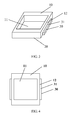
- FIG. 1 is a schematic three-dimensional view of Embodiment 1 of an insulating ring according to the present invention
- FIG. 2 is a schematic top view of Embodiment 1 of the insulating ring according to the present invention.
- FIG. 3 is a schematic three-dimensional view of Embodiment 2 of the insulating ring according to the present invention.
- FIG. 4 is a schematic top view of Embodiment 2 of the insulating ring according to the present invention.
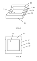
- FIG. 5 is a schematic three-dimensional view of Embodiment 3 of the insulating ring according to the present invention.
- FIG. 6 is a schematic top view of Embodiment 3 of the insulating ring according to the present invention.
- FIG. 7 is a schematic three-dimensional view of Embodiment 4 of the insulating ring according to the present invention.
- FIG. 8 is a schematic sectional view along Line A-A in FIG. 2 ;
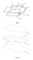
- FIG. 9 is a schematic three-dimensional view of an insulating ring assembly according to an embodiment of the present invention.
- FIG. 10 is a schematic three-dimensional exploded view of a package according to an embodiment of the present invention.
- the inventor analyzes the forming principle of silver migration in a PA, and improves the structure of an insulating ring from a conductive path by which the silver migration is cut off.
- the embodiment provides an insulating ring for packaging.
- a through hole 11 of the insulating ring drills through a top surface 10 and a bottom surface 20 of the insulating ring, to accommodate a chip (not shown).
- An outer sidewall of the insulating ring 1 has an outward extending protrusion 30 at a position where a pin is connected.
- a side surface 31 of the protrusion 30 which faces the top surface 10 is lower than the top surface 10.
- the pin (not shown) is disposed on the side surface 31, and an adhesive material layer and a surface metallization layer in the pin (not shown) are lower than the top surface 10.
- That the adhesive material layer and the surface metallization layer are lower than the top surface 10 may include two situations:
- the surface metallization layer is only laid on the side surface 31 while the adhesive material layer is laid on the surface metallization layer.
- An upper surface of the adhesive material layer is lower than the top surface 10.
- the surface of the insulating ring to which the pin is adhered needs to be processed firstly, that is, to form the surface metallization layer; therefore, without the surface metallization layer, the adhesion between the adhesive material and the insulating ring is insecure.
- the upper surface of the adhesive material is not higher than the top surface, and under the limitation of the surface metallization layer, the creeping of the adhesive material is limited to a horizontal direction.
- the surface metallization layer is laid on the side surface 31 and partially covers the outer sidewall 12 that is above the side surface 31, and the maximum height of the surface metallization layer on the outer sidewall 12 is lower than the top surface 10.
- the adhesive material layer is laid on the surface metallization layer, and the maximum height of the adhesive material layer on the outer sidewall 12 is lower than the top surface 10.
- the adhesive material creeps along the surface metallization layer, because the maximum height of the surface metallization layer is lower than the top surface 10, the final height of the adhesive material may not be higher than the top surface 10.
- a migration path for silver ions that may cause short circuit of the device is that the silver ions reach the top surface 10 from the adhesive material along the outer sidewall 12 that is above the side surface 31 and migrate to the through hole 11 of the insulating ring along the top surface 10, and then, owing to the effect of an electric field, the silver ions lead to conduction between the top surface 10 and the bottom surface 20 of the insulating ring, thereby causing the short circuit of the device.
- the adhesive material layer and the surface metallization layer in the pin are lower than the top surface.
- the adhesive material can creep along the surface metallization layer, if the adhesive material has already crept along the surface metallization layer after the device is used for a period of time, because the surface metallization layer and the adhesive material layer are both lower than the top surface 10, the adhesive material after creeping also cannot be higher than the top surface.
- the migration of the silver ions in the adhesive material is free from the limitation of the adhesive material, but during the process of using the device, the silver ions have no components of the electric field in a horizontal direction, and lateral migration is blocked by the outer sidewall 12 that is above the side surface 31.
- the electric field directs to the side surface 31 in a vertical direction and is opposite to the foregoing migration path of the silver ions. Therefore, the silver ions cannot pass around the outer sidewall 12 and the top surface 10 above the side surface 31 to enter the package, and accordingly, the top surface and the bottom surface of the insulating ring cannot be electrically connected, thereby ensuring the reliability of a PA device.
- the side surface 31 may be parallel to the top surface 10, and may also form an angle with the top surface 31, as long as the side surface 31 can be adhered to the pin.
- the upper surface and other side surfaces of the protrusion 30, which have no direct effect on the adhesion of the pin, are not limited by the embodiment of the present invention.
- the insulating ring 1 may be a square insulating ring, and may also be a circular insulating ring and so on, which may be specifically determined according to the shape of a metal frame.
- the protrusion 30 may extend to two ends of a square side where the protrusion 30 is located along a length direction of the square side.
- the side surface 31 may be maintained at a same height, and because such an insulating ring has a few sides, it is less difficult to process.
- the insulating ring may also be in a shape as shown in FIG. 3 and FIG. 4 .
- the protrusion 30 extends along a length direction of a square side where the protrusion 30 is located, and the length of the protrusion 30 along the length direction of the square side where the protrusion 30 is located is less than the length of the square side.
- One end of the protrusion 30 along the length direction of the square side where the protrusion 30 is located may be aligned with one end of the square side where the protrusion 30 is located; and it may also be as shown in FIG. 3 that, two ends of the protrusion 30 along the length direction of the square side where the protrusion 30 is located are both positioned within two ends of the square side where the protrusion 30 is located. The above two cases both have no impact on the connection of the pin.
- the protrusion 30 of the insulating ring may further extend along a length direction of a square side where the protrusion 30 is located, and is connected with the top surface 10 at positions of two ends along the length direction of the square side where the protrusion 30 is located.
- the protrusion 30 provides the side surface 31 at a position where the pin is connected, and the two ends of the protrusion 30 in the length direction extend towards the top surface 10 and are finally connected with the top surface 10.
- the protrusion 30 may approach to the top surface in a smooth and gradual transition manner (referring to FIG. 7 ), or in a stepped and abrupt transition manner (referring to FIG. 5 ), which both have no impact on the connection of the pin.
- the insulating ring 1 may be a ceramic ring, for example, the material may be aluminum oxide, and the insulating ring 1 may also be a plastic ring.
- the insulating ring may be processed by stamping, so that the insulating ring of the embodiment may be fabricated as along as a stamping die is modified, thereby causing a small impact on the cost of production.
- the pin is disposed on the side surface 31 and attached to the outer sidewall that is above the side surface 31.
- the pin includes the surface metallization layer 41, the adhesive material layer 42, a pin layer 43 and a protective layer 44 that wraps exposed portions of the surface metallization layer 41, the adhesive material layer 42 and the pin layer 43.
- the adhesive material layer 42 made of CuAg alloy is generally 15 to 20 ⁇ m in thickness
- the surface metallization layer 41 (the material thereof may be W) between the adhesive material layer 42 and the insulating ring 1 is generally 15 to 20 ⁇ m in thickness
- the pin layer 43 (the material thereof may be FeNi alloy) is generally about 100 ⁇ m in thickness
- an upper surface of the pin layer 43 is basically at the same level with the top surface 10, therefore, a distance between the side surface 31 and the top surface 10 is 130 to 140 ⁇ m
- the insulating ring 1 is generally greater than 200 ⁇ m in height.
- the protective layer 44 is electroplated at the exposed portions of the surface metallization layer 41, the adhesive material layer 42 and the pin layer 43 and the top surface 10 adjacent to the pin.
- the protective layer 44 may be made of NiCo alloy with good conductivity and is generally less than 3 ⁇ m in thickness.
- the adhesive material after creeping also cannot be higher than the top surface.
- the silver ions have no components of the electric field in the horizontal direction, and lateral migration is blocked by the outer sidewall that is above the side surface.
- the electric field directs to the side surface in the vertical direction and is opposite to the migration path of the silver ions. Therefore, the silver ions cannot pass around the outer sidewall and the top surface above the side surface to enter the package, and accordingly, the top surface and the bottom surface of the insulating ring cannot be electrically connected, thereby ensuring the reliability of the PA device.
- the insulating ring may also be used for the packaging of PCBs (printed circuit boards) of other chips and hybrid chips, and so on.
- PCBs printed circuit boards
- the foregoing insulating ring is also applicable to plastic packaging and hybrid module packaging, and so on.
- the embodiment provides an insulating ring assembly.
- the insulating ring assembly includes an insulating ring 1 and a pin 4 connected to the insulating ring 1.
- a through hole 11 of the insulating ring 1 drills through a top surface 10 and a bottom surface 20 of the insulating ring 1, to accommodate a chip (not shown).
- An outer sidewall of the insulating ring 1 has an outward extending protrusion 30 at a position where the pin 4 is connected.
- a side surface of the protrusion 30 which faces the top surface 10 is lower than the top surface 10.
- the pin 4 is disposed on the side surface, and an adhesive material layer and a surface metallization layer in the pin 4 are lower than the top surface 10. Exposed portions of each of other layers in the pin and the top surface 10 adjacent to the pin 4 are wrapped by a protective layer in the pin 4.
- the insulating ring 1 may be a square insulating ring, and may also be a circular insulating ring and so on, which may be specifically determined according to the shape of a metal frame.
- the protrusion 30 may extend to two ends of a square side where the protrusion 30 is located along a length direction of the square side; the protrusion 30 may also extend along the length direction of the square side where the protrusion 30 is located, and the length of the protrusion 30 along the length direction of the square side where the protrusion 30 is located is less than the length of the square side; and the protrusion 30 may also extend along the length direction of the square side where the protrusion 30 is located, and is connected with the top surface at positions of two ends along the length direction of the square side where the protrusion 30 is located.
- the insulating ring 1 may be a ceramic ring, for example, the material may be aluminum oxide, and the insulating ring may also be a plastic ring.
- the insulating ring may be processed by stamping, so that the insulating ring of the embodiment may be fabricated as along as a stamping die is modified, thereby causing a small impact on the cost of production.
- the pin 4 is disposed on the side surface and attached to the outer sidewall that is above the side surface.
- the pin 4 includes the surface metallization layer, the adhesive material layer, a pin layer and the protective layer that wraps the exposed portions of the surface metallization layer, the adhesive material layer and the pin layer.
- the adhesive material layer made of CuAg alloy is generally 15 to 20 ⁇ m in thickness
- the surface metallization layer (the material thereof may be W) between the adhesive material layer and the insulating ring 1 is generally 15 to 20 ⁇ m in thickness
- the pin layer (the material thereof may be FeNi alloy) is generally about 100 ⁇ m in thickness
- an upper surface of the pin layer is basically at the same level with the top surface, therefore, a distance between the side surface and the top surface is 130 to 140 ⁇ m
- the insulating ring 1 is generally greater than 200 ⁇ m in height.
- the protective layer is electroplated at the exposed portions of the surface metallization layer, the adhesive material layer and the pin layer and the top surface adjacent to the pin 4.
- the protective layer may be made of NiCo alloy with good conductivity and is generally less than 3 ⁇ m in thickness.
- the adhesive material after creeping also cannot be higher than the top surface.
- silver ions have no components of an electric field in a horizontal direction, and lateral migration is blocked by the outer sidewall that is above the side surface. The electric field directs to the side surface in a vertical direction and is opposite to the migration path of the silver ions. Therefore, the silver ions cannot pass around the outer sidewall and the top surface above the side surface to enter the package, and accordingly, the top surface and the bottom surface of the insulating cannot be electrically connected, thereby ensuring the reliability of a PA device.
- the embodiment provides a package.
- the package includes a conductive flange 2, an insulating ring 1 fixed on the conductive flange 2, a pin 4 connected to the insulating ring 1 and a seal cap 3 covering the insulating ring 1.
- a through hole of the insulating ring 1 drills through a top surface and a bottom surface of the insulating ring 1.
- a space is formed by the through hole, the conductive flange 2 and the seal cap 3 to accommodate a chip.
- An outer sidewall of the insulating ring 1 has an outward extending protrusion at a position where the pin 4 is connected.
- a side surface of the protrusion which faces the top surface is lower than the top surface.
- the pin 4 is disposed on the side surface, and an adhesive material layer and a surface metallization layer in the pin are lower than the top surface. Exposed portions of each of other layers in the pin 4 and the top surface adjacent to the pin are wrapped by a protective layer in the pin 4.
- the insulating ring 1 may be a square insulating ring as shown in FIG. 9 , and may also be a circular insulating ring and so on, which may be specifically determined according to the shape of a metal frame.
- the protrusion may extend to two ends of a square side of the insulating ring where the protrusion is located along a length direction of the square side; the protrusion may also extend along the length direction of the square side of the insulating ring where the protrusion is located, and the length of the protrusion along the length direction of the square side is less than the length of the square side; and the protrusion may also extend along the length direction of the square side of the insulating ring where the protrusion is located, and is connected with the top surface at positions of two ends along the length direction of the square side.
- the insulating ring 1 may be a ceramic ring, for example, of the material may be aluminum oxide, and the insulating ring 1 may also be a plastic ring.
- the insulating ring 1 may be processed by stamping, so that the insulating ring of the embodiment may be fabricated as along as a stamping die is modified, thereby causing less impact on the cost of production.
- the pin 4 is disposed on the side surface and attached to the outer sidewall that is above the side surface.
- the pin 4 includes the surface metallization layer, the adhesive material layer, a pin layer and the protective layer that wraps the exposed portions of the surface metallization layer, the adhesive material layer and the pin layer (referring to FIG. 8 ).
- the adhesive material layer made of CuAg alloy is generally 15 to 20 ⁇ m in thickness
- the surface metallization layer (the material thereof may be W) between the adhesive material layer and the insulating ring 1 is generally 15 to 20 ⁇ m in thickness
- the pin layer (the material thereof may be FeNi alloy) is generally about 100 ⁇ m in thickness
- an upper surface of the pin layer is basically at the same level as the top surface, therefore, a distance between the side surface and the top surface is 130 to 140 ⁇ m
- the insulating ring 1 is generally greater than 200 ⁇ m in height.
- the protective layer is electroplated at the exposed portions of the surface metallization layer, the adhesive material layer and the pin layer and the top surface adjacent to the pin.
- the protective layer may be made of NiCo alloy with good conductivity and is generally less than 3 ⁇ m in thickness.
- the material of the seal cap 3 may be ceramic, plastic or metal, and so on.
- the material of the conductive flange 2 may be copper, and so on.
- the adhesive material after creeping also cannot be higher than the top surface.
- silver ions have no components of an electric field in a horizontal direction, and lateral migration is blocked by the outer sidewall that is above the side surface. The electric field directs to the side surface in a vertical direction and is opposite to the migration path of the silver ions. Therefore, the silver ions cannot pass around the outer sidewall and the top surface above the side surface to enter the package, and accordingly, the top surface and the bottom surface of the insulating ring cannot be electrically connected, thereby ensuring the reliability of a PA device.
- the package may also be used for the packaging of PCBs of other chips and hybrid chips, and so on.
- the foregoing package is also applicable to plastic packaging and hybrid module packaging, and so on.
Landscapes
- Engineering & Computer Science (AREA)
- Microelectronics & Electronic Packaging (AREA)
- Lead Frames For Integrated Circuits (AREA)
- Die Bonding (AREA)
- Packaging Frangible Articles (AREA)
- Structures Or Materials For Encapsulating Or Coating Semiconductor Devices Or Solid State Devices (AREA)
Applications Claiming Priority (1)
| Application Number | Priority Date | Filing Date | Title |
|---|---|---|---|
| PCT/CN2011/075288 WO2011157171A2 (fr) | 2011-06-03 | 2011-06-03 | Bague isolante pour emballage, ensemble bague isolant, et enceinte |
Publications (1)
| Publication Number | Publication Date |
|---|---|
| EP2571047A2 true EP2571047A2 (fr) | 2013-03-20 |
Family
ID=44746736
Family Applications (1)
| Application Number | Title | Priority Date | Filing Date |
|---|---|---|---|
| EP11795137A Withdrawn EP2571047A2 (fr) | 2011-06-03 | 2011-06-03 | Bague isolante pour emballage, ensemble bague isolant, et enceinte |
Country Status (4)
| Country | Link |
|---|---|
| US (1) | US20130107469A1 (fr) |
| EP (1) | EP2571047A2 (fr) |
| CN (1) | CN102217059A (fr) |
| WO (1) | WO2011157171A2 (fr) |
Families Citing this family (8)
| Publication number | Priority date | Publication date | Assignee | Title |
|---|---|---|---|---|
| CN109901350A (zh) * | 2017-12-08 | 2019-06-18 | 深圳光峰科技股份有限公司 | 激光装置及投影设备 |
| CN109037161A (zh) * | 2018-06-15 | 2018-12-18 | 华为技术有限公司 | 一种法兰和半导体功率器件 |
| WO2020107153A1 (fr) | 2018-11-26 | 2020-06-04 | 华为技术有限公司 | Structure d'emballage et dispositif de communication |
| US11844178B2 (en) | 2020-06-02 | 2023-12-12 | Analog Devices International Unlimited Company | Electronic component |
| CN114582826A (zh) * | 2020-11-30 | 2022-06-03 | 上海华为技术有限公司 | 一种封装结构、封装方法 |
| CN114695544B (zh) * | 2020-12-31 | 2026-04-03 | 苏州能讯高能半导体有限公司 | 一种半导体器件及其制备方法 |
| USD1000958S1 (en) * | 2021-10-08 | 2023-10-10 | Oura Health Oy | Ring packaging insert |
| US20230317575A1 (en) * | 2022-03-30 | 2023-10-05 | Analog Devices, Inc. | Electronic device |
Family Cites Families (14)
| Publication number | Priority date | Publication date | Assignee | Title |
|---|---|---|---|---|
| JPH071789B2 (ja) * | 1986-03-04 | 1995-01-11 | 京セラ株式会社 | リ−ド付き電子部品 |
| EP0320618A1 (fr) * | 1987-12-14 | 1989-06-21 | BBC Brown Boveri AG | Boîtier pour un thyristor de puissance du type GTO |
| US5185653A (en) * | 1990-11-08 | 1993-02-09 | National Semiconductor Corporation | O-ring package |
| JP2833266B2 (ja) * | 1991-06-25 | 1998-12-09 | 富士電機株式会社 | 電力用半導体素子およびその製造方法 |
| US5309014A (en) * | 1992-04-02 | 1994-05-03 | Motorola Inc. | Transistor package |
| JP2792638B2 (ja) * | 1992-10-06 | 1998-09-03 | 京セラ株式会社 | 半導体素子収納用パッケージ |
| JP3309045B2 (ja) * | 1996-04-12 | 2002-07-29 | 京セラ株式会社 | リード付き電子部品 |
| US6072238A (en) * | 1999-04-07 | 2000-06-06 | Motorola, Inc. | Semiconductor component |
| US6462413B1 (en) * | 1999-07-22 | 2002-10-08 | Polese Company, Inc. | LDMOS transistor heatsink package assembly and manufacturing method |
| US6900525B2 (en) * | 2003-05-21 | 2005-05-31 | Kyocera America, Inc. | Semiconductor package having filler metal of gold/silver/copper alloy |
| JP4687769B2 (ja) * | 2008-10-20 | 2011-05-25 | Tdk株式会社 | 電子部品ユニット |
| CN102024770A (zh) * | 2009-09-18 | 2011-04-20 | 中芯国际集成电路制造(上海)有限公司 | 半导体芯片封装结构及封装方法 |
| CN101777523A (zh) * | 2010-01-19 | 2010-07-14 | 无锡小天鹅陶瓷有限责任公司 | 特高压大功率晶闸管元件管壳 |
| CN201812808U (zh) * | 2010-10-08 | 2011-04-27 | 潮州三环(集团)股份有限公司 | 带凸台的陶瓷封装基座 |
-
2011
- 2011-06-03 CN CN2011800008099A patent/CN102217059A/zh active Pending
- 2011-06-03 WO PCT/CN2011/075288 patent/WO2011157171A2/fr not_active Ceased
- 2011-06-03 EP EP11795137A patent/EP2571047A2/fr not_active Withdrawn
-
2012
- 2012-12-20 US US13/721,439 patent/US20130107469A1/en not_active Abandoned
Non-Patent Citations (1)
| Title |
|---|
| See references of WO2011157171A2 * |
Also Published As
| Publication number | Publication date |
|---|---|
| US20130107469A1 (en) | 2013-05-02 |
| WO2011157171A3 (fr) | 2012-05-03 |
| WO2011157171A2 (fr) | 2011-12-22 |
| CN102217059A (zh) | 2011-10-12 |
Similar Documents
| Publication | Publication Date | Title |
|---|---|---|
| EP2571047A2 (fr) | Bague isolante pour emballage, ensemble bague isolant, et enceinte | |
| US9530712B2 (en) | Power electronic switching device and assembly | |
| US20180092201A1 (en) | High-frequency module | |
| US8963315B2 (en) | Semiconductor device with surface electrodes | |
| US10790258B2 (en) | Electronic device and mounting structure of the same | |
| US9064818B2 (en) | Semiconductor device | |
| US10192806B2 (en) | Semiconductor device | |
| TW201340261A (zh) | 半導體裝置及其製造方法 | |
| US20180096937A1 (en) | Semiconductor device | |
| KR20150109284A (ko) | 반도체 장치 및 그 제조 방법 | |
| KR101766082B1 (ko) | 파워모듈 | |
| KR20140100904A (ko) | 반도체 장치 | |
| US9905490B2 (en) | Semiconductor device | |
| KR101688350B1 (ko) | 반도체 장치 및 그 제조 방법 | |
| US8741695B2 (en) | Semiconductor device and method of manufacturing the same | |
| US9159676B2 (en) | Semiconductor module | |
| US20180096910A1 (en) | Molded resin-sealed power semiconductor device | |
| JP6115505B2 (ja) | 電子装置 | |
| KR101516371B1 (ko) | 접합 홈을 구비하는 칩 원판 및 이를 봉지하기 위한 봉지부재 | |
| US12389528B2 (en) | Module | |
| EP4485523B1 (fr) | Boîtier d'interconnexion et module de puissance | |
| US20200258851A1 (en) | Electronic module | |
| CN206282841U (zh) | 半导体装置 | |
| US20150001696A1 (en) | Semiconductor die carrier structure and method of manufacturing the same | |
| JP2015005687A (ja) | 樹脂パッケージとこの樹脂パッケージを用いた電子機器 |
Legal Events
| Date | Code | Title | Description |
|---|---|---|---|
| PUAI | Public reference made under article 153(3) epc to a published international application that has entered the european phase |
Free format text: ORIGINAL CODE: 0009012 |
|
| 17P | Request for examination filed |
Effective date: 20121213 |
|
| AK | Designated contracting states |
Kind code of ref document: A2 Designated state(s): AL AT BE BG CH CY CZ DE DK EE ES FI FR GB GR HR HU IE IS IT LI LT LU LV MC MK MT NL NO PL PT RO RS SE SI SK SM TR |
|
| STAA | Information on the status of an ep patent application or granted ep patent |
Free format text: STATUS: THE APPLICATION HAS BEEN WITHDRAWN |
|
| 18W | Application withdrawn |
Effective date: 20130731 |