EP2571056A2 - Ensemble caméra à double face - Google Patents
Ensemble caméra à double face Download PDFInfo
- Publication number
- EP2571056A2 EP2571056A2 EP12183090A EP12183090A EP2571056A2 EP 2571056 A2 EP2571056 A2 EP 2571056A2 EP 12183090 A EP12183090 A EP 12183090A EP 12183090 A EP12183090 A EP 12183090A EP 2571056 A2 EP2571056 A2 EP 2571056A2
- Authority
- EP
- European Patent Office
- Prior art keywords
- bsi
- fsi
- semiconductor die
- disposed
- array
- Prior art date
- Legal status (The legal status is an assumption and is not a legal conclusion. Google has not performed a legal analysis and makes no representation as to the accuracy of the status listed.)
- Withdrawn
Links
Images


Classifications
-
- H—ELECTRICITY
- H10—SEMICONDUCTOR DEVICES; ELECTRIC SOLID-STATE DEVICES NOT OTHERWISE PROVIDED FOR
- H10F—INORGANIC SEMICONDUCTOR DEVICES SENSITIVE TO INFRARED RADIATION, LIGHT, ELECTROMAGNETIC RADIATION OF SHORTER WAVELENGTH OR CORPUSCULAR RADIATION
- H10F39/00—Integrated devices, or assemblies of multiple devices, comprising at least one element covered by group H10F30/00, e.g. radiation detectors comprising photodiode arrays
- H10F39/10—Integrated devices
- H10F39/12—Image sensors
- H10F39/18—Complementary metal-oxide-semiconductor [CMOS] image sensors; Photodiode array image sensors
- H10F39/182—Colour image sensors
-
- H—ELECTRICITY
- H10—SEMICONDUCTOR DEVICES; ELECTRIC SOLID-STATE DEVICES NOT OTHERWISE PROVIDED FOR
- H10F—INORGANIC SEMICONDUCTOR DEVICES SENSITIVE TO INFRARED RADIATION, LIGHT, ELECTROMAGNETIC RADIATION OF SHORTER WAVELENGTH OR CORPUSCULAR RADIATION
- H10F39/00—Integrated devices, or assemblies of multiple devices, comprising at least one element covered by group H10F30/00, e.g. radiation detectors comprising photodiode arrays
- H10F39/011—Manufacture or treatment of image sensors covered by group H10F39/12
- H10F39/018—Manufacture or treatment of image sensors covered by group H10F39/12 of hybrid image sensors
-
- H—ELECTRICITY
- H10—SEMICONDUCTOR DEVICES; ELECTRIC SOLID-STATE DEVICES NOT OTHERWISE PROVIDED FOR
- H10F—INORGANIC SEMICONDUCTOR DEVICES SENSITIVE TO INFRARED RADIATION, LIGHT, ELECTROMAGNETIC RADIATION OF SHORTER WAVELENGTH OR CORPUSCULAR RADIATION
- H10F39/00—Integrated devices, or assemblies of multiple devices, comprising at least one element covered by group H10F30/00, e.g. radiation detectors comprising photodiode arrays
- H10F39/10—Integrated devices
- H10F39/12—Image sensors
- H10F39/199—Back-illuminated image sensors
-
- H—ELECTRICITY
- H10—SEMICONDUCTOR DEVICES; ELECTRIC SOLID-STATE DEVICES NOT OTHERWISE PROVIDED FOR
- H10F—INORGANIC SEMICONDUCTOR DEVICES SENSITIVE TO INFRARED RADIATION, LIGHT, ELECTROMAGNETIC RADIATION OF SHORTER WAVELENGTH OR CORPUSCULAR RADIATION
- H10F39/00—Integrated devices, or assemblies of multiple devices, comprising at least one element covered by group H10F30/00, e.g. radiation detectors comprising photodiode arrays
- H10F39/80—Constructional details of image sensors
- H10F39/802—Geometry or disposition of elements in pixels, e.g. address-lines or gate electrodes
- H10F39/8023—Disposition of the elements in pixels, e.g. smaller elements in the centre of the imager compared to larger elements at the periphery
-
- H—ELECTRICITY
- H10—SEMICONDUCTOR DEVICES; ELECTRIC SOLID-STATE DEVICES NOT OTHERWISE PROVIDED FOR
- H10F—INORGANIC SEMICONDUCTOR DEVICES SENSITIVE TO INFRARED RADIATION, LIGHT, ELECTROMAGNETIC RADIATION OF SHORTER WAVELENGTH OR CORPUSCULAR RADIATION
- H10F39/00—Integrated devices, or assemblies of multiple devices, comprising at least one element covered by group H10F30/00, e.g. radiation detectors comprising photodiode arrays
- H10F39/80—Constructional details of image sensors
- H10F39/805—Coatings
- H10F39/8053—Colour filters
-
- H—ELECTRICITY
- H10—SEMICONDUCTOR DEVICES; ELECTRIC SOLID-STATE DEVICES NOT OTHERWISE PROVIDED FOR
- H10F—INORGANIC SEMICONDUCTOR DEVICES SENSITIVE TO INFRARED RADIATION, LIGHT, ELECTROMAGNETIC RADIATION OF SHORTER WAVELENGTH OR CORPUSCULAR RADIATION
- H10F39/00—Integrated devices, or assemblies of multiple devices, comprising at least one element covered by group H10F30/00, e.g. radiation detectors comprising photodiode arrays
- H10F39/80—Constructional details of image sensors
- H10F39/806—Optical elements or arrangements associated with the image sensors
- H10F39/8063—Microlenses
-
- H—ELECTRICITY
- H10—SEMICONDUCTOR DEVICES; ELECTRIC SOLID-STATE DEVICES NOT OTHERWISE PROVIDED FOR
- H10F—INORGANIC SEMICONDUCTOR DEVICES SENSITIVE TO INFRARED RADIATION, LIGHT, ELECTROMAGNETIC RADIATION OF SHORTER WAVELENGTH OR CORPUSCULAR RADIATION
- H10F39/00—Integrated devices, or assemblies of multiple devices, comprising at least one element covered by group H10F30/00, e.g. radiation detectors comprising photodiode arrays
- H10F39/80—Constructional details of image sensors
- H10F39/809—Constructional details of image sensors of hybrid image sensors
-
- H—ELECTRICITY
- H10—SEMICONDUCTOR DEVICES; ELECTRIC SOLID-STATE DEVICES NOT OTHERWISE PROVIDED FOR
- H10F—INORGANIC SEMICONDUCTOR DEVICES SENSITIVE TO INFRARED RADIATION, LIGHT, ELECTROMAGNETIC RADIATION OF SHORTER WAVELENGTH OR CORPUSCULAR RADIATION
- H10F39/00—Integrated devices, or assemblies of multiple devices, comprising at least one element covered by group H10F30/00, e.g. radiation detectors comprising photodiode arrays
- H10F39/80—Constructional details of image sensors
- H10F39/811—Interconnections
Definitions
- the present invention generally relates generally to image sensors, and in particular, but not exclusively, relates to camera modules including a rear facing camera and a front facing camera.
- Mobile electronic devices with image capture abilities such as cellular telephones, are becoming increasingly popular. Some mobile devices are capable of capturing image data from two directions (e.g., from the "front” and “rear” sides of the device).
- the invention provides an apparatus according to claim 1 and a method according to claim 11.
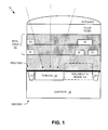
- FIG. 1 illustrates an FSI complementary metal-oxide-semiconductor ("CMOS") imaging pixel according to an embodiment of the disclosure.
- CMOS complementary metal-oxide-semiconductor
- FIG. 2 is a hybrid cross sectional/circuit illustration of a BSI imaging pixel according to an embodiment of the disclosure.
- FIG. 3 is a cross-section view of a dual-facing camera assembly according to an embodiment of the disclosure.
- FIG. 4 is a flow chart illustrating a process for fabricating a dual-facing camera assembly according to an embodiment of the disclosure.
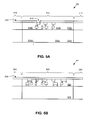
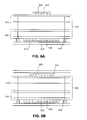
- FIG. 5A - FIG. 5D are block diagrams of image wafers forming a dual camera assembly according to an embodiment of the disclosure.
- FIG. 6A - FIG. 6D illustrate processing operations for packaging a dual-facing camera assembly according to an embodiment of the disclosure.
- FIG. 7 is a cross-section view of a dual-facing camera assembly according to an embodiment of the disclosure.
- Embodiments of an apparatus, system and method for utilizing and creating a dual-facing camera assembly are described herein.
- numerous specific details are set forth to provide a thorough understanding of the embodiment.
- One skilled in the relevant art will recognize however, that the techniques described herein can be practiced without one or more of the specific details, components, materials, etc. In other instances, well-known structure, materials or operations are not shown or described in detail to avoid obscuring certain aspects.
- references throughout this specification to "one embodiment” or “an embodiment” means that a particular feature, structure or characteristic described in connection with the embodiment is included in at least one embodiment of the present invention.
- the appearances of the phrases “in one embodiment” or “in an embodiment” in various places throughout this specification are not necessarily all referring to the same embodiment.
- the particular features, structures, or characteristics may be combined in any suitable manner in one or more embodiments.
- Directional terminology such as top, bottom, over and under are used with reference to the orientation of the figure(s) being described, but should not be interpreted as any kind of limitation on the orientation of the embodiment.
- FIG. 1 illustrates an FSI complementary metal-oxide-semiconductor ("CMOS") imaging pixel according to an embodiment of the disclosure.
- the frontside of imaging pixel 100 is the side of substrate 105 upon which the pixel circuitry is disposed and over which metal stack 110 for redistributing signals is formed.
- the metal layers e.g., metal layer M1 and M2 are patterned in such a manner as to create an optical passage through which light incident on the frontside of imaging pixel 100 can reach the photosensitive or photodiode (“PD”) region 115.
- the frontside may further include a color filter layer to implement a color sensor and a microlens to focus the light onto PD region 115.
- imaging pixel 100 includes pixel circuitry disposed within pixel circuitry region 125 adjacent to PD region 115.
- This pixel circuitry provides a variety of functionality for regular operation of imaging pixel 100.
- pixel circuitry region 125 may include circuitry to commence acquisition of an image charge within PD region 115, to reset the image charge accumulated within PD region 115 to ready imaging pixel 100 for the next image, or to transfer out the image data acquired by imaging pixel 100.
- pixel circuitry region 125 is positioned immediately adjacent to PD region 115.
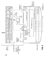
- FIG. 2 is a hybrid cross sectional/circuit illustration of a BSI imaging pixel according to an embodiment of the disclosure.
- BSI imaging pixel 200 includes substrate 205, color filter 210, microlens 215, PD region 220, interlinking diffusion region 225, pixel circuitry region 230, pixel circuitry layers 235, and a metal stack 240.
- the illustrated embodiment of pixel circuitry region 230 includes a 4T pixel (other pixel designs may be substituted), as well as other circuitry 231 (e.g., gain circuitry, ADC circuitry, gamma control circuitry, exposure control circuitry, etc.), disposed over a diffusion well 245.
- floating diffusion 250 is disposed within diffusion well 245 and coupled between transfer transistor T1 and the gate of SF transistor T3.
- the illustrated embodiment of metal stack 240 includes two metal layers M1 and M2 separated by intermetal dielectric layers 241 and 243. Although FIG. 2 illustrates only a two layer metal stack, metal stack 240 may include more or less layers for routing signals over the frontside of imaging pixel 200.
- a passivation or pinning layer 240 is disposed over interlinking diffusion region 225.
- shallow trench isolations isolate BSI imaging pixel 200 from adjacent pixels (not illustrated).
- imaging pixel 200 is photosensitive to light 280 incident on the backside of its semiconductor die.
- pixel circuitry region 230 may be positioned in an overlapping configuration with photodiode region 220.
- pixel circuitry can be placed adjacent to interlinking diffusion region 225 and between photodiode region 220 and the die frontside without obstructing light 280 from reaching photodiode region 220.
- pixel circuitry region 220 can be enlarged to accommodate additional or larger components without detracting from the fill factor of the image sensor.
- BSI imaging pixel 200 further enables other circuits 231, such as gain control or ADC circuitry, to be placed in close proximity to their respective photodiode region 220 without decreasing the sensitivity of the pixel.
- gain control and ADC circuitry By inserting gain control and ADC circuitry in close proximity to each PD region 220, circuit noise can be reduced and noise immunity improved due to shorter electrical interconnections between PD region 220 and the additional in-pixel circuitry.
- the backside illumination configuration of the illustrated embodiment provides greater flexibility to route signals over the frontside of imaging pixel 200 within metal stack 240 without interfering with light 280.
- a shutter signal is routed within metal stack 240 to the pixels of a BSI imaging array (including pixel 200).
- pixel circuit regions 230 over PD regions 220 of adjacent pixels within a BSI pixel array can be grouped to create communal die real estate.
- This communal die real estate can support shared circuitry (or inter-pixel circuitry) in addition to the basic 3T, 4T, 5T, etc. pixel circuitry.
- some pixels can share their unused die real estate above their PD regions to an adjacent pixel requiring additional pixel circuitry space for larger or more advanced in-pixel circuitry.
- other circuitry 231 may overlap two or more PD regions 220 and may even be shared by one or more pixels.
- substrate 205 is doped with P type dopants.
- substrate 205 and the epitaxial layers grown thereon may be referred to as a P substrate.
- diffusion well 245 is a P+ well implant while photodiode region 220, interlinking diffusion region 225, and floating diffusion 250 are N type doped.
- Floating diffusion 250 is doped with an opposite conductivity type dopant as diffusion well 245 to generate a p-n junction within diffusion well 245, thereby electrically isolating floating diffusion 250.
- diffusion well 245 is also N type doped, while photodiode region 220, interlinking diffusion region 225, and floating diffusion 250 have an opposite P type conductivity.
- FIG. 3 is a cross-section view of a dual-facing camera assembly according to an embodiment of the disclosure.
- dual-facing camera assembly 300 includes first imaging system 310 and second imaging system 350.
- First imaging system 310 includes array of FSI imaging pixels. Each pixel of said array is formed from substrate 311 and metal stack 312. For example, each pixel of the FSI array may have a PD region formed in substrate 311 that receives light that passes through metal stack 312, similar to FSI imaging pixel 100 shown in FIG. 1 . Furthermore, each pixel of the FSI array may utilize a corresponding color filter 314 and microlens 315.
- First imaging system 310 further includes adhesive glue 316 and cover glass 317 disposed over said microlenses.
- Second imaging system 350 includes array of BSI imaging pixels 305. Each pixel of said array is formed from substrate 351 and metal stack 352. For example, each pixel of the BSI array may have a PD region formed in substrate 351 and disposed between metal stack 352 and backside p+ layer 353, similar to the BSI imaging pixel shown in FIG. 2 . Furthermore, each pixel may utilize a corresponding color filter 354 and microlens 355. Second imaging system 350 further includes adhesive glue 356 and cover glass 357 disposed over said microlenses.
- first imaging system 310 is bonded to the topside of second imaging system 350 via bonding layer 320.
- electromagnetic radiation incident to opposing sides of dual-facing camera assembly 300 is incident to the photosensitive region of one of the arrays of image sensors.
- BSI imaging pixels may include pixel circuitry placed in an overlapping configuration with its photodiode region, as opposed to the side-by-side configurations FSI imaging pixels; thus the pixel circuitry regions of BSI imaging pixels can be enlarged to accommodate additional or larger components without detracting from the fill factor of the image sensor. Therefore in some embodiments, BSI imaging system 350 is capable of capturing image data with a higher image resolution compared to FSI imaging system 310.
- the redistribution layer (“RDL”) for BSI image sensor 350 may be achieved with chip scale packing ("CSP") or thru-silicon via (“TSV”) process to make metal stack 352 of second imaging system 350 assessable to metal pads 360.
- metal pads 360 are deposited onto the front side of semiconductor substrate 312 by way of sputtering, collimated sputtering, low pressure sputtering, reactive sputtering, electroplating, chemical vapor deposition or evaporation or any functionally equivalent process known in the art.
- Metal pads 360 provide access for substrate 380 to the imaging data captured by imaging systems 310 and 350.
- TSVs 361 and 362 are formed through metal stack 312 and substrate 311 to operatively couple metal layer 352 to metal pads 360.
- metal stack 312 and substrate 311 in the region that is not direct under cover glass 317 may be used in the TSV process since the substrate and metal stack area taken up by FSI pixel array 311 is found in the region under cover glass 317.
- FIG. 4 is a flow chart illustrating a process for fabricating a dual-facing camera assembly according to an embodiment of the disclosure.
- Flow diagrams as illustrated herein provide examples of sequences of various process actions. Although shown in a particular sequence or order, unless otherwise specified, the order of the actions can be modified. Thus, the illustrated implementations should be understood only as examples, and the illustrated processes can be performed in a different order, and some actions may be performed in parallel. Additionally, one or more actions can be omitted in various embodiments of the invention; thus, not all actions are required in every implementation. Other process flows are possible.
- FIG. 5A - FIG. 5D are block diagrams of image wafers forming a dual camera assembly according to an embodiment of the disclosure, and are to be viewed in the context of the process flow shown in FIG. 4 .
- the fabrication of an FSI image sensor may comprise conventional techniques right up to the fabrication of the back-end-of-the-line ("BEOL") components including diffusion implants, silicides, pixel transistor circuitry and metal stack.
- BEOL back-end-of-the-line
- FIG. 5A is an illustration of fabricated FSI image sensor wafer 505.
- Region 510 comprises FSI image sensor regions 520a-b and unused regions 530a-b.
- the passive and active semiconductor elements in an image sensor such as the CMOS transistors found in the pixel array, readout circuitry and other circuits are fabricated in substrate region 520a.
- Metal stack 520b is fabricated over substrate 520a. In this embodiment, no semiconductor elements are formed in substrate region 520b. Unused regions 530a-b may include dielectric layers.
- Passivation layer 540 is formed over metal stack 520b, with passivation opening 545 formed to expose metal pads on the top metal interconnect layer. In other embodiments, passivation layer 540 is omitted.
- metal stack 520b includes two metal interconnect layers separated by intermetal dielectric layers. Although FIG. 5A illustrates a two-layer metal stack, metal stack 520b may include more or less metal interconnect layers for routing signals above the top side of substrate 520a.
- the metal interconnect layers comprises a metal such as aluminum, copper, or other alloy.
- metal interconnect layers are formed by way of sputtering, collimated sputtering, low pressure sputtering, reactive sputtering, electroplating, chemical vapor deposition or evaporation.
- the fabrication of a BSI image sensor die may comprise conventional techniques right up to the fabrication of the BEOL components including diffusion implants, silicides, pixel transistor circuitry and metal stack.
- FIG. 5B is an illustration of fabricated BSI image wafer 555.
- region 510 in FIG. 5A which comprises FSI image sensor die 520 and unused regions 530 is relatively the same size as BSI image sensor die 560, so that when FSI image sensor wafer 505 and BSI image sensor wafer 555 are bonded together, the physical center of FSI image sensor die 520 lines up with the physical center of BSI image sensor 560.
- the passive and active semiconductor elements of the image sensor such as the CMOS transistors found in the pixel array, readout circuitry and other circuits are fabricated in substrate 570.
- Metal stack 580 is formed on top of substrate 570. In the illustrated embodiment, metal stack 580 includes two metal interconnect layers separated by intermetal dielectric layers. Passivation 590 is formed over metal stack 580. In other embodiments, passivation 590 is omitted.
- the passive and active elements of FSI image sensor die 520 and BSI image sensor die 560 are formed in substrate 520 and 570 respectively.
- semiconductor elements of FSI image sensor die 510 and BSI image sensor die 560 may be formed in an epitaxial layer.
- semiconductor elements of FSI image sensor die 510 and BSI image sensor die 560 may be formed in an epitaxial layer with a substrate layer formed under said epitaxial layer.
- the bottom side of the FSI image sensor wafer is bonded to the top side of the BSI image sensor wafer using a bonding oxide.
- the bottom side of FSI image sensor wafer 505 is bonded to the top side of BSI image sensor wafer 555 using bonding oxide 595.
- the size of BSI image sensor die 560 is approximately the same size as FSI image sensor die 520 and unused regions 530.
- FSI image sensor die 520 and unused regions 530 are positioned so that the physical center of FSI image sensor die 520 lines up with the physical center of BSI image sensor die 560 after both wafers are bonded together.
- at this stage of processing FSI image sensor wafer 505 and BSI image sensor wafer 555 each have the same thickness (e.g., approximately 400 ⁇ m).
- the backside of the BSI wafer is thinned via known methods such as chemical-mechanical planarization.
- the thinning of the backside of substrate 570 is shown in FIG. 5D .
- FSI image sensor wafer 505 acts as the handling wafer for BSI image sensor wafer 555, thus a separate handling wafer is not necessary (a handle wafer is used as a handle to hold a partially fabricated imaging pixel array while thinning its backside).
- BSI image sensor wafer 555 will have a thickness that is less than that of FSI image wafer.
- backside p+ layer of substrate 570 is a p-type layer; in other embodiments of the invention, said backside layer may be an n-type layer or may be omitted.
- both image sensors are subject to a deposition of an anti-reflective coating.
- the anti-reflective coating may be omitted in other embodiments of the invention. In other embodiments of the invention, the anti-reflective coating may be omitted.
- Protective tape may be placed over the top side of FSI image sensor wafer 505 to protect the top metal interconnect layer.
- FIG. 6A - FIG. 6D illustrate processing operations for packaging a dual-facing camera assembly according to an embodiment of the disclosure.
- FIG. 6A is a cross-section view illustrating dual-facing image sensor 600 including FSI image sensor wafer 610 bonded to BSI image sensor wafer 620.
- Color filters 650 are formed over each FSI image sensor pixel in FSI image sensor wafer 610.
- Microlenses 655 are formed over color filters 650.
- Color filters 630 are formed over each BSI image sensor pixel in BSI image sensor wafer 620.
- Microlenses 635 are formed over color filters 630.
- FIG. 6A illustrates that BSI image wafer 620 has more "pixels" than FSI image wafer 610 - i.e., BSI image wafer 620 may capture image data at a higher resolution than FSI image wafer 610.
- the thickness of FSI image sensor wafer excluding color filters 650 and microlenses 655 is approximately 200 ⁇ m
- the thickness of BSI image sensor wafer 620, excluding color filters 630 and microlenses 635 is approximately 2 ⁇ m.
- color filters 630 and microlenses 635 on BSI image wafer 620 After the formation of color filters 630 and microlenses 635 on BSI image wafer 620, adhesive spacer 640 and cover glass 645 are installed to protect said microlenses, while color filters 650 and microlenses 655 are formed.
- FIG. 6B is a cross-section view illustrating dual facing image sensor wafer 600 having a cover glass installed to protect microlenses 655 of FSI image wafer 610.
- adhesive spacer 660 and cover glass 665 are installed over microlenses 655.
- FSI image wafer 610 includes fewer pixels (and thus, fewer color filters and microlenses) than BSI image wafer 620.
- cover glass 665 is formed to expose areas of the top metal of FSI wafer 610 not used by the FSI image sensor die. As described below, this area is to be utilized during the formation of a redistribution layer ("RDL").
- RDL redistribution layer
- FIG. 6C is a cross-section view illustrating dual-facing image sensor wafer 600 after the formation of the RDL and TSV connections fabricated to couple the metal layer 670 of BSI image sensor die to metal pads 675.
- a TSV process is used to form TSVs 671 which provide access to metal layer 670 of BSI image wafer 620.
- CSP processes may be used to operatively couple metal layer 670 to metal pads 675.
- Dual-facing image sensor wafer 600 may be die sawed using known methods before or after metal pads 675 are formed.
- FIG. 6D is a cross-section view illustrating solder balls 680 which couple metal pads 675 to a substrate such as printed circuit board (“PCB") 690.
- PCB 690 may be operatively coupled to the metal layers of both FSI image sensor and BSI image sensor to control each imaging system and receive captured image data.
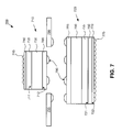
- FIG. 7 is a cross-section view illustrating a dual-facing camera assembly according to an embodiment of the disclosure.
- dual-facing camera assembly 700 includes two package dies, FSI image sensor 710 and BSI image sensor 720.
- dual-facing camera assembly 700 comprises two packaged dies operatively coupled to a PCB substrate.
- the photosensitive region of FSI image sensor 710 is formed under frontside 711 of substrate 730.
- substrate 730 comprises an epitaxial layer.
- Metal stack 735 is formed on frontside 711 of substrate 730.
- Metal stack 735 includes one or more metal interconnect layers separated by dielectric layers.
- Color filter 740 is formed on metal stack 735 and microlens 745 is formed on color filter 740.
- RDL 780 (discussed below) is formed on backside 712 of substrate 730.
- the photosensitive region of BSI image sensor 720 is formed under frontside 721 of substrate 750.
- substrate 750 comprises an epitaxial layer.
- Metal stack 755 is formed on frontside 721 of substrate 750.
- Metal stack 755 comprises one or more metal interconnect layers separated by dielectric layers.
- Handle substrate 760 is bonded to substrate 750 before BSI image sensor 720 is die-sawed on the silicon wafer.
- a handle substrate is used as a handle to hold a partially fabricated imaging pixel while thinning its backside.
- Handle substrate 760 may be formed from a silicon wafer comprised of multiple handle substrate (alternatively referred to herein as a handle wafer) that is bonded to BSI image sensor 720 during fabrication.
- Color filter 770 is formed and microlenses 775 are formed on color filter 770.
- RDL 785 is formed on the frontside of BSI image sensor 720.
- Solder balls 790 are formed on the backside of RDL 780 and front side of RDL 785, and may be soldered to a substrate such as PCB 795.
- the thickness of dual-facing camera assembly 700 is greater than the thickness of dual-facing camera assembly 600 in FIG. 6D , since dual-facing camera assembly 700 uses a separate handle substrate for BSI image sensor 720 instead of using an FSI image sensor as the BSI image sensor's handle substrate (as described above).
Landscapes
- Solid State Image Pick-Up Elements (AREA)
- Transforming Light Signals Into Electric Signals (AREA)
- Studio Devices (AREA)
Applications Claiming Priority (1)
| Application Number | Priority Date | Filing Date | Title |
|---|---|---|---|
| US13/235,121 US8497536B2 (en) | 2011-09-16 | 2011-09-16 | Dual-facing camera assembly |
Publications (2)
| Publication Number | Publication Date |
|---|---|
| EP2571056A2 true EP2571056A2 (fr) | 2013-03-20 |
| EP2571056A3 EP2571056A3 (fr) | 2014-09-03 |
Family
ID=47115255
Family Applications (1)
| Application Number | Title | Priority Date | Filing Date |
|---|---|---|---|
| EP12183090.5A Withdrawn EP2571056A3 (fr) | 2011-09-16 | 2012-09-05 | Ensemble caméra à double face |
Country Status (4)
| Country | Link |
|---|---|
| US (3) | US8497536B2 (fr) |
| EP (1) | EP2571056A3 (fr) |
| CN (1) | CN103066081B (fr) |
| TW (1) | TWI566338B (fr) |
Cited By (5)
| Publication number | Priority date | Publication date | Assignee | Title |
|---|---|---|---|---|
| FR3026227A1 (fr) * | 2014-09-18 | 2016-03-25 | Commissariat Energie Atomique | Dispositif d'acquisition d'images 3d |
| WO2016143288A1 (fr) * | 2015-03-12 | 2016-09-15 | Sony Corporation | Dispositif d'imagerie, procédé de fabrication et dispositif électronique |
| JP2016171297A (ja) * | 2015-03-12 | 2016-09-23 | ソニー株式会社 | 固体撮像装置および製造方法、並びに電子機器 |
| US20220037382A1 (en) * | 2018-12-20 | 2022-02-03 | Sony Semiconductor Solutions Corporation | Backside-illumination solid-state image pickup apparatus and backside-illumination solid-state image-pickup-apparatus manufacturing method, image pickup apparatus, and electronic equipment |
| US11316065B2 (en) * | 2015-07-24 | 2022-04-26 | Artilux, Inc. | Multi-wafer based light absorption apparatus and applications thereof |
Families Citing this family (39)
| Publication number | Priority date | Publication date | Assignee | Title |
|---|---|---|---|---|
| US8497536B2 (en) | 2011-09-16 | 2013-07-30 | Omnivision Technologies, Inc. | Dual-facing camera assembly |
| US8716823B2 (en) * | 2011-11-08 | 2014-05-06 | Aptina Imaging Corporation | Backside image sensor pixel with silicon microlenses and metal reflector |
| US8906320B1 (en) | 2012-04-16 | 2014-12-09 | Illumina, Inc. | Biosensors for biological or chemical analysis and systems and methods for same |
| KR102072509B1 (ko) | 2013-06-03 | 2020-02-04 | 삼성전자주식회사 | 그룹 리코딩 방법, 저장 매체 및 전자 장치 |
| TWI662670B (zh) * | 2013-08-30 | 2019-06-11 | Xintec Inc. | 電子元件封裝體及其製造方法 |
| US9711555B2 (en) | 2013-09-27 | 2017-07-18 | Taiwan Semiconductor Manufacturing Company, Ltd. | Dual facing BSI image sensors with wafer level stacking |
| US9679936B2 (en) | 2014-02-27 | 2017-06-13 | Semiconductor Components Industries, Llc | Imaging systems with through-oxide via connections |
| US9349767B2 (en) | 2014-04-16 | 2016-05-24 | Semiconductor Components Industries, Llc | Image sensors with through-oxide via structures |
| US9293495B2 (en) | 2014-05-05 | 2016-03-22 | Semiconductor Components Industries, Llc | Imaging circuitry with robust scribe line structures |
| US9324755B2 (en) | 2014-05-05 | 2016-04-26 | Semiconductor Components Industries, Llc | Image sensors with reduced stack height |
| US9147711B1 (en) * | 2014-06-16 | 2015-09-29 | Amazon Technologies, Inc. | Camera module including flip chip image sensor |
| TWI585959B (zh) * | 2014-08-13 | 2017-06-01 | 精材科技股份有限公司 | 晶片封裝體及其製造方法 |
| US9818776B2 (en) | 2015-04-08 | 2017-11-14 | Semiconductor Components Industries, Llc | Integrating bond pad structures with light shielding structures on an image sensor |
| US10217783B2 (en) | 2015-04-08 | 2019-02-26 | Semiconductor Components Industries, Llc | Methods for forming image sensors with integrated bond pad structures |
| WO2016172863A1 (fr) * | 2015-04-29 | 2016-11-03 | 华为技术有限公司 | Module d'appareil photographique |
| CN105140251A (zh) * | 2015-07-03 | 2015-12-09 | 豪威科技(上海)有限公司 | 一种背照式图像传感器晶圆、芯片及其制造方法 |
| CN105609513A (zh) * | 2015-10-29 | 2016-05-25 | 上海集成电路研发中心有限公司 | 双面cmos图像传感器芯片及其制造方法 |
| US9786705B2 (en) | 2015-12-21 | 2017-10-10 | Qualcomm Incorporated | Solid state image sensor with extended spectral response |
| US10121812B2 (en) | 2015-12-29 | 2018-11-06 | Taiwan Semiconductor Manufacturing Co., Ltd. | Stacked substrate structure with inter-tier interconnection |
| US9875388B2 (en) * | 2016-02-26 | 2018-01-23 | Taiwan Semiconductor Manufacturing Company, Ltd. | Fingerprint sensor device and method |
| US9818791B1 (en) * | 2016-10-04 | 2017-11-14 | Omnivision Technologies, Inc. | Stacked image sensor |
| CN106409855B (zh) * | 2016-11-23 | 2019-04-09 | 山东华芯电子有限公司 | 一种双面图像传感器 |
| CN106430075B (zh) * | 2016-11-23 | 2017-11-07 | 山东鸿荣电子有限公司 | 一种传感器的制造方法 |
| CN106373974B (zh) * | 2016-11-24 | 2019-10-18 | 江苏骏龙光电科技股份有限公司 | 一种具有参考电容的传感器件 |
| CN106373973B (zh) * | 2016-11-24 | 2019-11-05 | 江苏骏龙光电科技股份有限公司 | 一种抗干扰图像传感器 |
| CN106505074A (zh) * | 2016-11-24 | 2017-03-15 | 南通沃特光电科技有限公司 | 一种图像传感器的制造方法 |
| CN106409856B (zh) * | 2016-11-24 | 2019-09-20 | 江苏天楹之光光电科技有限公司 | 一种制造具有参考电容的传感器的方法 |
| CN106506969B (zh) * | 2016-11-29 | 2019-07-19 | Oppo广东移动通信有限公司 | 摄像模组、通过其进行人像追踪的方法以及电子设备 |
| KR101926007B1 (ko) * | 2016-12-21 | 2018-12-06 | 남동욱 | 양면 이미지 센서 및 그 제조 방법 |
| CN106851059A (zh) * | 2016-12-30 | 2017-06-13 | 奇鋐科技股份有限公司 | 摄影模组 |
| US10237475B2 (en) * | 2017-01-15 | 2019-03-19 | Asia Vital Components Co., Ltd. | Camera module |
| JP2018117027A (ja) * | 2017-01-18 | 2018-07-26 | ソニーセミコンダクタソリューションズ株式会社 | 固体撮像素子、電子装置、および、固体撮像素子の製造方法 |
| KR102275684B1 (ko) | 2017-04-18 | 2021-07-13 | 삼성전자주식회사 | 반도체 패키지 |
| US10861829B2 (en) * | 2017-12-26 | 2020-12-08 | Illumina, Inc. | Sensor system |
| CN110299375B (zh) * | 2019-07-08 | 2021-06-18 | 芯盟科技有限公司 | 半导体结构及其形成方法 |
| CN212587504U (zh) * | 2020-06-09 | 2021-02-23 | 深圳市大疆创新科技有限公司 | 半导体封装结构 |
| US11532524B2 (en) | 2020-07-27 | 2022-12-20 | Taiwan Semiconductor Manufacturing Co., Ltd. | Integrated circuit test method and structure thereof |
| JP2022114447A (ja) * | 2021-01-26 | 2022-08-05 | ファスフォードテクノロジ株式会社 | ダイボンディング装置および半導体装置の製造方法 |
| KR102877798B1 (ko) * | 2021-05-17 | 2025-10-30 | 삼성전자주식회사 | 반도체 패키지 |
Citations (1)
| Publication number | Priority date | Publication date | Assignee | Title |
|---|---|---|---|---|
| US20110080474A1 (en) * | 2009-10-02 | 2011-04-07 | Olympus Corporation | Image pickup device, image pickup unit, and endoscope |
Family Cites Families (13)
| Publication number | Priority date | Publication date | Assignee | Title |
|---|---|---|---|---|
| DE10394380B4 (de) * | 2002-12-10 | 2021-05-06 | Sata Gmbh & Co. Kg | Einwandiger Spritzpistolenbecher |
| US7619683B2 (en) * | 2003-08-29 | 2009-11-17 | Aptina Imaging Corporation | Apparatus including a dual camera module and method of using the same |
| KR100539259B1 (ko) * | 2004-04-26 | 2005-12-27 | 삼성전자주식회사 | 자동으로 정렬되는 렌즈를 포함하는 이미지 센서 모듈, 그제조방법 및 렌즈의 자동 초점 조절방법 |
| US6898030B1 (en) * | 2004-06-17 | 2005-05-24 | Prodisc Technology Inc. | Camera lens assembly |
| KR100674911B1 (ko) * | 2004-08-06 | 2007-01-26 | 삼성전자주식회사 | 이미지 센서 카메라 모듈 및 그 제조방법 |
| KR100674833B1 (ko) * | 2005-02-16 | 2007-01-26 | 삼성전기주식회사 | 카메라 모듈 |
| US7539412B2 (en) | 2006-05-17 | 2009-05-26 | Terrasem Co. Ltd. | Camera module with first and second image sensor chips, holders and lens |
| TWI320857B (en) * | 2006-09-07 | 2010-02-21 | Ether Precision Inc | The small optics lens which don't must forcusing and its method |
| US8101978B2 (en) * | 2008-02-08 | 2012-01-24 | Omnivision Technologies, Inc. | Circuit and photo sensor overlap for backside illumination image sensor |
| US8054355B2 (en) * | 2008-10-16 | 2011-11-08 | Omnivision Technologies, Inc. | Image sensor having multiple sensing layers |
| US8227288B2 (en) * | 2009-03-30 | 2012-07-24 | Taiwan Semiconductor Manufacturing Company, Ltd. | Image sensor and method of fabricating same |
| TWI457687B (zh) * | 2010-03-26 | 2014-10-21 | Ability Entpr Co Ltd | 影像投影及擷取系統與方法 |
| US8497536B2 (en) * | 2011-09-16 | 2013-07-30 | Omnivision Technologies, Inc. | Dual-facing camera assembly |
-
2011
- 2011-09-16 US US13/235,121 patent/US8497536B2/en active Active
-
2012
- 2012-08-10 TW TW101129095A patent/TWI566338B/zh active
- 2012-09-05 EP EP12183090.5A patent/EP2571056A3/fr not_active Withdrawn
- 2012-09-05 CN CN201210325412.3A patent/CN103066081B/zh active Active
-
2013
- 2013-06-26 US US13/927,495 patent/US8900912B2/en active Active
-
2014
- 2014-10-30 US US14/528,991 patent/US9305962B2/en active Active
Patent Citations (1)
| Publication number | Priority date | Publication date | Assignee | Title |
|---|---|---|---|---|
| US20110080474A1 (en) * | 2009-10-02 | 2011-04-07 | Olympus Corporation | Image pickup device, image pickup unit, and endoscope |
Cited By (7)
| Publication number | Priority date | Publication date | Assignee | Title |
|---|---|---|---|---|
| FR3026227A1 (fr) * | 2014-09-18 | 2016-03-25 | Commissariat Energie Atomique | Dispositif d'acquisition d'images 3d |
| WO2016143288A1 (fr) * | 2015-03-12 | 2016-09-15 | Sony Corporation | Dispositif d'imagerie, procédé de fabrication et dispositif électronique |
| JP2016171297A (ja) * | 2015-03-12 | 2016-09-23 | ソニー株式会社 | 固体撮像装置および製造方法、並びに電子機器 |
| US20180166490A1 (en) * | 2015-03-12 | 2018-06-14 | Sony Corporation | Imaging device, manufacturing method, and electronic device |
| US11316065B2 (en) * | 2015-07-24 | 2022-04-26 | Artilux, Inc. | Multi-wafer based light absorption apparatus and applications thereof |
| US20220037382A1 (en) * | 2018-12-20 | 2022-02-03 | Sony Semiconductor Solutions Corporation | Backside-illumination solid-state image pickup apparatus and backside-illumination solid-state image-pickup-apparatus manufacturing method, image pickup apparatus, and electronic equipment |
| US12230662B2 (en) * | 2018-12-20 | 2025-02-18 | Sony Semiconductor Solutions Corporation | Backside-illumination solid-state image pickup apparatus, image pickup apparatus, and electronic equipment including embedment members |
Also Published As
| Publication number | Publication date |
|---|---|
| US20150054106A1 (en) | 2015-02-26 |
| CN103066081A (zh) | 2013-04-24 |
| US20130069188A1 (en) | 2013-03-21 |
| TWI566338B (zh) | 2017-01-11 |
| US9305962B2 (en) | 2016-04-05 |
| US8900912B2 (en) | 2014-12-02 |
| EP2571056A3 (fr) | 2014-09-03 |
| TW201314843A (zh) | 2013-04-01 |
| US8497536B2 (en) | 2013-07-30 |
| CN103066081B (zh) | 2016-12-28 |
| US20130285183A1 (en) | 2013-10-31 |
Similar Documents
| Publication | Publication Date | Title |
|---|---|---|
| US8497536B2 (en) | Dual-facing camera assembly | |
| US12520614B2 (en) | Solid-state image sensor, method for producing solid-state image sensor, and electronic device | |
| US10930699B2 (en) | Method and apparatus for image sensor packaging | |
| US10003759B2 (en) | Vertically stacked image sensor | |
| KR101579372B1 (ko) | 고체 촬상 장치 및 고체 촬상 장치의 제조 방법 | |
| US20210391371A1 (en) | Imaging device and electronic device | |
| US8698934B2 (en) | Solid-state image sensing device, camera module, and solid-state image sensing device manufacturing method | |
| US9635228B2 (en) | Image sensors with interconnects in cover layer | |
| JP2013201188A (ja) | 固体撮像装置 | |
| US9312292B2 (en) | Back side illumination image sensor and manufacturing method thereof | |
| EP2245665B1 (fr) | Capteur imageur rétroéclairé pourvu d'un substrat support et d'une couche de redistribution | |
| US10622391B2 (en) | Imaging systems with through-oxide via connections | |
| HK1181192A (en) | Dual-facing camera assembly | |
| HK1181192B (en) | Dual-facing camera assembly | |
| US20240145515A1 (en) | Stacked integrated circuit dies and interconnect structures | |
| US11201187B2 (en) | CMOS image sensor packaging structure and fabrication method thereof, and camera device |
Legal Events
| Date | Code | Title | Description |
|---|---|---|---|
| PUAI | Public reference made under article 153(3) epc to a published international application that has entered the european phase |
Free format text: ORIGINAL CODE: 0009012 |
|
| AK | Designated contracting states |
Kind code of ref document: A2 Designated state(s): AL AT BE BG CH CY CZ DE DK EE ES FI FR GB GR HR HU IE IS IT LI LT LU LV MC MK MT NL NO PL PT RO RS SE SI SK SM TR |
|
| AX | Request for extension of the european patent |
Extension state: BA ME |
|
| RIC1 | Information provided on ipc code assigned before grant |
Ipc: H01L 27/146 20060101AFI20140328BHEP |
|
| PUAL | Search report despatched |
Free format text: ORIGINAL CODE: 0009013 |
|
| AK | Designated contracting states |
Kind code of ref document: A3 Designated state(s): AL AT BE BG CH CY CZ DE DK EE ES FI FR GB GR HR HU IE IS IT LI LT LU LV MC MK MT NL NO PL PT RO RS SE SI SK SM TR |
|
| AX | Request for extension of the european patent |
Extension state: BA ME |
|
| RIC1 | Information provided on ipc code assigned before grant |
Ipc: H01L 27/146 20060101AFI20140729BHEP |
|
| 17P | Request for examination filed |
Effective date: 20150210 |
|
| RBV | Designated contracting states (corrected) |
Designated state(s): AL AT BE BG CH CY CZ DE DK EE ES FI FR GB GR HR HU IE IS IT LI LT LU LV MC MK MT NL NO PL PT RO RS SE SI SK SM TR |
|
| 17Q | First examination report despatched |
Effective date: 20171211 |
|
| STAA | Information on the status of an ep patent application or granted ep patent |
Free format text: STATUS: THE APPLICATION HAS BEEN WITHDRAWN |
|
| 18W | Application withdrawn |
Effective date: 20180405 |