EP2571114A2 - Dispositif de puissance combiné - Google Patents
Dispositif de puissance combiné Download PDFInfo
- Publication number
- EP2571114A2 EP2571114A2 EP11192097A EP11192097A EP2571114A2 EP 2571114 A2 EP2571114 A2 EP 2571114A2 EP 11192097 A EP11192097 A EP 11192097A EP 11192097 A EP11192097 A EP 11192097A EP 2571114 A2 EP2571114 A2 EP 2571114A2
- Authority
- EP
- European Patent Office
- Prior art keywords
- hole
- module
- pin
- partial
- main body
- Prior art date
- Legal status (The legal status is an assumption and is not a legal conclusion. Google has not performed a legal analysis and makes no representation as to the accuracy of the status listed.)
- Granted
Links
Images


Classifications
-
- H—ELECTRICITY
- H01—ELECTRIC ELEMENTS
- H01R—ELECTRICALLY-CONDUCTIVE CONNECTIONS; STRUCTURAL ASSOCIATIONS OF A PLURALITY OF MUTUALLY-INSULATED ELECTRICAL CONNECTING ELEMENTS; COUPLING DEVICES; CURRENT COLLECTORS
- H01R9/00—Structural associations of a plurality of mutually-insulated electrical connecting elements, e.g. terminal strips or terminal blocks; Terminals or binding posts mounted upon a base or in a case; Bases therefor
- H01R9/22—Bases, e.g. strip, block, panel
- H01R9/24—Terminal blocks
- H01R9/2408—Modular blocks
-
- H—ELECTRICITY
- H01—ELECTRIC ELEMENTS
- H01R—ELECTRICALLY-CONDUCTIVE CONNECTIONS; STRUCTURAL ASSOCIATIONS OF A PLURALITY OF MUTUALLY-INSULATED ELECTRICAL CONNECTING ELEMENTS; COUPLING DEVICES; CURRENT COLLECTORS
- H01R13/00—Details of coupling devices of the kinds covered by groups H01R12/70 or H01R24/00 - H01R33/00
- H01R13/02—Contact members
- H01R13/22—Contacts for co-operating by abutting
- H01R13/24—Contacts for co-operating by abutting resilient; resiliently-mounted
-
- H—ELECTRICITY
- H01—ELECTRIC ELEMENTS
- H01R—ELECTRICALLY-CONDUCTIVE CONNECTIONS; STRUCTURAL ASSOCIATIONS OF A PLURALITY OF MUTUALLY-INSULATED ELECTRICAL CONNECTING ELEMENTS; COUPLING DEVICES; CURRENT COLLECTORS
- H01R31/00—Coupling parts supported only by co-operation with counterpart
- H01R31/06—Intermediate parts for linking two coupling parts, e.g. adapter
- H01R31/065—Intermediate parts for linking two coupling parts, e.g. adapter with built-in electric apparatus
-
- H—ELECTRICITY
- H01—ELECTRIC ELEMENTS
- H01R—ELECTRICALLY-CONDUCTIVE CONNECTIONS; STRUCTURAL ASSOCIATIONS OF A PLURALITY OF MUTUALLY-INSULATED ELECTRICAL CONNECTING ELEMENTS; COUPLING DEVICES; CURRENT COLLECTORS
- H01R13/00—Details of coupling devices of the kinds covered by groups H01R12/70 or H01R24/00 - H01R33/00
- H01R13/62—Means for facilitating engagement or disengagement of coupling parts or for holding them in engagement
- H01R13/627—Snap or like fastening
- H01R13/6271—Latching means integral with the housing
- H01R13/6272—Latching means integral with the housing comprising a single latching arm
-
- H—ELECTRICITY
- H01—ELECTRIC ELEMENTS
- H01R—ELECTRICALLY-CONDUCTIVE CONNECTIONS; STRUCTURAL ASSOCIATIONS OF A PLURALITY OF MUTUALLY-INSULATED ELECTRICAL CONNECTING ELEMENTS; COUPLING DEVICES; CURRENT COLLECTORS
- H01R13/00—Details of coupling devices of the kinds covered by groups H01R12/70 or H01R24/00 - H01R33/00
- H01R13/66—Structural association with built-in electrical component
- H01R13/70—Structural association with built-in electrical component with built-in switch
- H01R13/71—Contact members of coupling parts operating as switch, e.g. linear or rotational movement required after mechanical engagement of coupling part to establish electrical connection
Definitions
- the present invention relates to power devices, and more particularly to combinative power devices.
- Consumer electronic products such as notebooks, personal digital assistants (PDA), mobile phones, MP3 players, and so on, are trending toward smaller sizes continuously, which thereby promotes higher demand for easily-portable electric power connectors, for example, a power supply, a battery charger, or a transformer. Therefore, the electric power connectors of consumer electronic products need to be made with smaller sizes and less weight, and more convenient for shipment. Furthermore, they must be durable in order to sustain long-term carrying and frequent usage.
- PDA personal digital assistants
- the light emitting diode power supply when a light emitting diode power supply is disposed in a light emitting diode lamp holder, for the lamp holders with different numbers of light emitting diode modules, the light emitting diode power supply must have corresponding numbers of contact points to power each light emitting diode module. Therefore, when the number of the light emitting diode modules changes, the manufacturing process for the light emitting diode power supply must be modified.
- any of the battery charger, the transformer or the light emitting diode power supply has an AC-to-DC portion and a portion to further process the direct current and output the processed direct current.
- the AC-to-DC portion usually needs to be performed with safety inspection. Therefore, when a new type of battery charger, transformer or light emitting diode power supply is developed, the entire of the new type of battery charger, transformer or light emitting diode power supply must be implemented with safety inspection, thereby delaying the time-to-market.
- the present invention provides a combinative power device.
- the present invention provides a combinative power device, including an AC-to-DC module including a first joint portion; and a DC-to-DC module having a second joint portion and coupled to the AC-to-DC module by the second joint portion with the first joint portion electrically, wherein the DC-to-DC module acts as a removable module which can be removable from the AC-to-DC module to enable the AC-to-DC module to cooperate with different types of the DC-to-DC module.
- the present invention provides a combinative power device, including an AC-to-DC module including at least one projected portion and a cavity formed on the side wall of one end of the AC-to-DC module, wherein a flange is disposed on the outer edge of the at least one projected portion; and a DC-to-DC module including at least one concave portion and a flexible slice formed on the side wall of one end of the DC-to-DC module, wherein a flange is disposed on the outer edge of the at least one concave portion and a projected piece is disposed on the flexible slice to be locked by the cavity, the at least one concave portion receiving the at least one projected portion, the flange of the at least one concave portion locking the flange of the at least one projected portion.
- the present invention provides a combinative power device, including an AC-to-DC module including a first hole and a second hole formed thereon, the first hole including a first partial hole and a second partial hole, the second hole including a first partial hole and a second partial hole, widths or diameters of the first partial hole of the first hole and the first partial hole of the second hole being larger than widths or diameters of the second partial hole of the first hole and the second partial hole of the second hole respectively, the first partial hole of the first hole connecting one end of the second partial hole of the first hole, the second partial hole of the second hole connecting one side of the first partial hole of the second hole; and a DC-to-DC module including a main body, a first pin and a second pin, wherein the first pin and the second pin are disposed on the main body, widths or diameters of first portions of the first pin and the second pin which are close to the main body being smaller than widths or diameters of second portions of the first pin and the second pin which are far from the main body respectively,
- One advantage of the present invention is that the DC-to-DC module or the AC-to-DC module of the combinative power device of the present invention can be flexibly replaced with DC-to-DC modules or AC-to-DC modules of other specifications.
- Another advantage of the present invention is that the combinative power device of the present invention can enhance the robustness of the entire structure in the horizontal direction or the vertical direction.
- Still another advantage of the present invention is that the combinative power device of the present invention can shorten the time-to-market for the power device.
- Yet another advantage of the present invention is that the present invention can decrease the weight of the transformers or the battery chargers needed to be taken along by the user.
- the present invention provides a combinative power device, which includes an AC-to-DC module and a DC-to-DC module.
- the AC-to-DC module and the DC-to-DC module may be combined through chutes or through the locking mechanism between holes and pins.
- the combinative power device of the present invention may be applied to light emitting diode power supplies, battery chargers or transformers with changeable converters.
- the battery chargers may include but be not limited to lithium battery chargers, AA battery chargers, AAA battery chargers, etc.
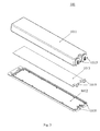
- the combinative power device 10 may include an AC-to-DC module 101 and a DC-to-DC module 102, the inner AC-to-DC circuits of which is well-known and therefore is omitted.
- the exemplary combinative power device shown in the present embodiment is employed for the light emitting diode power supply, for illustrating the present invention but not for limiting the present invention. Therefore, the combinative power device shown in Fig. 1 may also be applied to the battery charger (as shown in Fig. 10 ) or the transformer with the changeable converter.
- the AC-to-DC module 101 and the DC-to-DC module 102 may be combined through chutes.
- one end of the AC-to-DC module 101 may be slid into the grooves in the DC-to-DC module 102 to combine both.
- Figs. 3 and 5 illustrate the structure of the AC-to-DC module 101.
- the AC-to-DC module 101 may include a first joint portion.
- the AC-to-DC module 101 may include an upper case 1011, a lower case 1012 and a circuit board 1013 to dispose circuits and electronic elements (not shown) thereon.
- the circuit board 1013 is disposed on the lower case 1012 while the upper case 1011 is disposed on the circuit board 1013.
- Conductive slices 1019 are disposed at one end of the circuit board 1013.
- the material of the conductive slices 1019 may be metal or alloy.
- the first joint portion is disposed on the side wall of one end of the upper case 1011 and may include projected portions 1014.
- Flanges 1015 are disposed on the outer edges of the projected portions 1014.
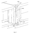
- the centers of the projected portions 1014 are disposed with openings for the conductive slices (which will be described hereinafter) of the DC-to-DC module 102 to partially pass therethrough and electrically couple with the conductive slices 1019 of the AC-to-DC module 101.
- the openings are adjacent to the conductive slices 1019.
- a cavity 1016 is disposed on the side wall of the upper case 1011 and between the projected portions 1014 to lock a projected piece (which will be described hereinafter) of the DC-to-DC module 102.
- projected portions 1017 are disposed on the side wall of one end of the lower case 1012.
- Flanges 1018 are disposed on the outer edges of the projected portions 1017.
- a cavity 1020 is disposed on the side wall of the lower case 1012 and between the projected portions 1017.
- the sizes and the contours of the projected portions 1017, the flanges 1018 and the cavity 1020 correspond to those of the projected portions 1014, the flanges 1015 and the cavity 1016 respectively so as to form continuous structures.
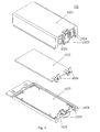
- the first joint portion is utilized to joint a removable module.
- the removable module may include a DC-to-DC module 102, which may include an upper case 1021, a lower case 1022 and a circuit board 1023 to dispose circuits and electronic elements (not shown) thereon.
- the DC-to-DC module 102 may include a second joint portion.
- the circuit board 1023 is disposed on the lower case 1022 while the upper case 1021 is disposed on the circuit board 1023.
- Conductive slices 1030 are disposed at one end of the circuit board 1023.
- the material of the conductive slices 1030 may be metal or alloy.
- the second joint portion is disposed on the side wall of one end of the upper case 1021 to joint the first joint portion.
- the second joint portion is disposed with concave portions 1024 to receive the projected portions 1014 of the AC-to-DC module 101.
- Flanges 1025 are disposed on the outer edges of the concave portions 1024 to lock the flanges 1015 of the AC-to-DC module 101.
- the centers of the concave portions 1024 are disposed with openings for the conductive slices 1030 to partially pass therethrough and electrically couple with the conductive slices 1019 of the AC-to-DC module 101. The openings are adjacent to the conductive slices 1030.
- a cavity 1031 is disposed on the side wall of the upper case 1021 and between the concave portions 1024, and a flexible slice 1026 is disposed in the cavity 1031.
- a projected piece 1027 is disposed on the flexible slice 1026 to be locked by the cavity 1016 of the AC-to-DC module 101, such that the robustness of the entire structure in the vertical direction may be enhanced through the locking mechanism between the cavity 1016 and the projected piece 1027.
- the flexible slice 1026 is flexible, such that the projected piece 1027 will be detached from the cavity 1016, and the projected portions 1014 and the flanges 1015 of the AC-to-DC module 101 will be able to be slid out of the concave portions 1024 of the DC-to-DC module 102 when the flexible slice 1026 is shifted towards the inner of the cavity 1031. Therefore, the DC-to-DC module 102 will be able to be detached from the AC-to-DC module 101.
- concave portions 1028 are disposed on the side wall of one end of the lower case 1022 to receive the projected portions 1017 of the AC-to-DC module 101.
- Flanges 1029 are disposed on the outer edges of the concave portions 1028 to lock the flanges 1018 of the AC-to-DC module 101.
- the sizes and the contours of the concave portions 1028 and the flanges 1029 correspond to those of the concave portions 1024 and the flanges 1025 respectively so as to form continuous structures.
- the conductive slice 1019 and the conductive slice 1030 may contact each other, so as to form electrical coupling.
- the flanges 1018 and the flanges 1029 may lock each other, so as to improve the robustness of the entire structure in the horizontal direction.
- the flanges 1015 and the flanges 1025 may also lock each other (not shown).
- the cavity 1016 may lock the projected piece 1027, such that the robustness of the entire structure in the vertical direction will be further enhanced.
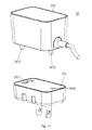
- Fig. 11 illustrates a diagram of a combinative power device in accordance with another embodiment of the present invention.
- the exemplary combinative power device shown in the present invention may be utilized for the transformers with changeable converters, for illustrating the present invention but not for limiting the present invention. Therefore, the combinative power device shown in Fig. 11 may also be applied to the battery chargers or the light emitting diode power supply.
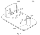
- the combinative power device 20 may include an AC-to-DC module 201 and a DC-to-DC module 202.
- a plug in the AC-to-DC module 201 may be rotatable, such that the plug may be rotated out of or into the case.
- the DC-to-DC module 202 may include a pin 2022 and a pin 2023 while the AC-to-DC module 201 may include a hole 2017 and a hole 2018.
- the pin 2022 and the pin 2023 may be inserted into the hole 2018 and the hole 2017 respectively, and the DC-to-DC module 202 may be moved a predetermined distance towards the hole 2017 and rotated counter clockwise, so as to render the pin 2022 and the pin 2023 to be locked by the hole 2018 and the hole 2017 respectively and combine the AC-to-DC module 201 and the DC-to-DC module 202.
- the DC-to-DC module 202 may include a main body 2021, the pin 2022 and the pin 2023.
- the pin 2022 and the pin 2023 are disposed on the main body 2021.
- the pin 2022 and the pin 2023 may be disposed asymmetrically.
- Both the pin 2023 and the pin 2022 have two different diameters or widths. The diameter or the width of one end of the pin 2023 and the pin 2022 which is far from the main body is larger than that of another end of the pin 2023 and the pin 2022 which is close to the main body.
- both ends of the pin 2023 may be cylindrical.
- the end of the pin 2023 which is close to the main body may be cylindrical while the end of the pin 2023 which is far from the main body may be geometric pillar shaped.
- the geometric pillar may include but be not limited to cylinder and rectangular prism, for example square prism.
- the end of the pin 2022 which is close to the main body may be cylindrical.
- the end of the pin 2022 which is far from the main body may be chamfered-edge cylinder shaped.
- the AC-to-DC module 201 may include an upper case 2011, conductive slices 2012, a fixing member 2013, a fixing rack 2014, a rotatable rack 2015 and a lower case 2016.
- the rotatable rack 2015 is disposed on the lower case 2016 while the fixing member 2013 and the fixing rack 2014 are disposed on the rotatable rack 2015.
- the conductive slices 2012 are disposed on the fixing member 2013 while the upper case 2011 is disposed on the conductive slices 2012.
- the upper case 2011 may include a hole 2017 and a hole 2018.
- the hole 2017 may include a first partial hole, for example a geometric hole, which may include but be not limited to a circular hole and a rectangular hole such as a square hole, and a second partial hole, for example a long curved hole, so as to be inserted by the pin 2023 of the DC-to-DC module 202.
- the first partial hole connects with one end of the second partial hole.
- the width or the diameter of the first partial hole is larger than that of the second partial hole.
- the widths or the diameters of the first partial hole and the second partial hole substantially match those of the end of the pin 2023 which is far from the main body and the end of the pin 2023 which is close to the main body respectively, such that after the end of the pin 2023 which is far from the main body is inserted into the first partial hole for example the geometric hole, if the end of the pin 2023 which is close to the main body passes through the geometric hole, the end of the pin 2023 which is close to the main body can enter the second partial hole such as the long curved hole and the DC-to-DC module 202 can be rotated counter clockwise around the pin 2022 to render the end of the pin 2023 which is close to the main body to be slid into the long curved hole and perform locking mechanism.
- the hole 2018 may include a first partial hole, for example a chamfered-edge circular hole, and a second partial hole, such as a semicircular hole.
- the second partial hole connects with one side of the first partial hole.
- the chamfered-edge portion of the semicircular hole connects with the chamfered-edge portion of the chamfered-edge circular hole.
- the width or the diameter of the first partial hole is larger than that of the second partial hole.
- the shapes and the sizes of the first partial hole and the second partial hole substantially match the section shapes and the sizes thereof of the end of the pin 2022 which is far from the main body and the end of the pin 2022 which is close to the main body respectively, such that after the end of the pin 2022 which is far from the main body is inserted into the first partial hole for example the chamfered-edge circular hole, if the end of the pin 2022 which is close to the main body passes through the chamfered-edge circular hole, the end of the pin 2022 which is close to the main body can be slid into the second partial hole such as the semicircular hole to perform the rotation of the DC-to-DC module 202. While the end of the pin 2023 which is close to the main body initially enters the long curved hole, the end of the pin 2022 which is close to the main body will be slid into the semicircular hole.
- the upper case 2011 further includes a baffle 2019 and a baffle 2020 formed on the lower surface thereof.
- the baffle 2019 surrounds the hole 2017 while the baffle 2020 surrounds the hole 2018.
- the rotatable rack 2015 is inserted into two through holes in the lower case 2016, such that the rotatable rack 2015 may be sandwiched in between the lower case 2016 and the fixing member 2013 and the fixing rack 2014 to perform the rotation.
- the conductive slices 2012 contact the shorter ends of the prongs of the rotatable rack 2015 which pass through the fixing member 2013 at one end and contact the pin 2022 or the pin 2023 which passes through the hole 2018 or the hole 2017 at the other end, so as to form electrical coupling between the prongs of the rotatable rack 2015 and the pin 2022 or the pin 2023.
- the material of the conductive slices 2012 may be metal or alloy.
- the present invention employs the chutes or the locking mechanism between the holes and the pins to combine the AC-to-DC module and the DC-to-DC module, so as to provide the combinative power device.
- the aforementioned combinative power device may be applied to the light emitting diode power supplies, the transformers with changeable converters or the battery chargers. Therefore, the DC-to-DC module or the AC-to-DC module may be replaced with the DC-to-DC module or the AC-to-DC module of other specifications.
- the combinative power device is a battery charger
- the DC-to-DC module with battery charging cavity can be replaced with a DC-to-DC module having different types of battery charging cavities for different types of batteries.
- a DC-to-DC module with AA battery charging cavity can be replaced with a DC-to-DC module with AAA battery or lithium battery charging cavity.
- the AC-to-DC module can also be replaced with an AC-to-DC module having plugs of different specifications.
- the combinative power device is a light emitting diode power supply
- the DC-to-DC module can be replaced with a DC-to-DC module for different numbers of light emitting diodes.
- the combinative power device is a transformer with a changeable converter
- the AC-to-DC module can be replaced with an AC-to-DC module having converters of different specifications.
- the AC-to-DC module can cooperate with different kinds of DC-to-DC modules to facilitate its scalability and convenience for sales because the DC-to-DC module of the combinative power device of the present invention is replaceable and only the AC-to-DC module needs to be performed with safety inspection. Therefore, the combinative power device of the present invention can shorten the time-to-market for the power device.
- the DC-to-DC module or the AC-to-DC module of the combinative power device of the present invention can be replaced with DC-to-DC modules or AC-to-DC modules of other specifications, the user is not required to carry different battery chargers or transformers for different mobile devices and only needs to carry necessary modules to replace, thereby the weight of the transformers or the battery chargers needed to be taken along by the user can be decreased.
Landscapes
- Charge And Discharge Circuits For Batteries Or The Like (AREA)
- Rectifiers (AREA)
- Dc-Dc Converters (AREA)
Applications Claiming Priority (1)
| Application Number | Priority Date | Filing Date | Title |
|---|---|---|---|
| TW100133521A TWI454027B (zh) | 2011-09-16 | 2011-09-16 | 組合式電源裝置 |
Publications (3)
| Publication Number | Publication Date |
|---|---|
| EP2571114A2 true EP2571114A2 (fr) | 2013-03-20 |
| EP2571114A3 EP2571114A3 (fr) | 2013-08-28 |
| EP2571114B1 EP2571114B1 (fr) | 2016-11-09 |
Family
ID=45421877
Family Applications (1)
| Application Number | Title | Priority Date | Filing Date |
|---|---|---|---|
| EP11192097.1A Not-in-force EP2571114B1 (fr) | 2011-09-16 | 2011-12-06 | Dispositif de puissance combiné |
Country Status (4)
| Country | Link |
|---|---|
| US (1) | US8638562B2 (fr) |
| EP (1) | EP2571114B1 (fr) |
| JP (1) | JP5656123B2 (fr) |
| TW (1) | TWI454027B (fr) |
Families Citing this family (1)
| Publication number | Priority date | Publication date | Assignee | Title |
|---|---|---|---|---|
| CN103683905A (zh) * | 2012-09-07 | 2014-03-26 | 鸿富锦精密工业(深圳)有限公司 | 电压转换器 |
Family Cites Families (16)
| Publication number | Priority date | Publication date | Assignee | Title |
|---|---|---|---|---|
| US10019A (en) * | 1853-09-13 | Improvement in the manufacture of plain and figured fabrics | ||
| US2127473A (en) * | 1934-02-20 | 1938-08-16 | Sacco James | Electric connecter |
| US3120985A (en) * | 1961-04-19 | 1964-02-11 | Hubbell Inc Harvey | Electrical connector having selective key means for different voltages |
| JP2004173458A (ja) * | 2002-11-22 | 2004-06-17 | Kyocera Corp | 電源装置 |
| DE102005052667B4 (de) * | 2005-03-22 | 2008-01-17 | Dehn + Söhne Gmbh + Co. Kg | Steckbare Gerätekombination, insbesondere zum Schutz vor Überspannungen |
| CN100454666C (zh) * | 2005-08-23 | 2009-01-21 | 鸿富锦精密工业(深圳)有限公司 | 电子设备组合装置 |
| US7303440B2 (en) * | 2005-10-03 | 2007-12-04 | Stull Michael F | Universal battery charger/power source adapter |
| US7642671B2 (en) * | 2006-04-28 | 2010-01-05 | Acco Brands Usa Llc | Power supply system providing two output voltages |
| ES2320611B1 (es) * | 2006-11-06 | 2010-01-12 | Inoitulos, S.L. | "dispositivo adaptador para la carga de aparatos electronicos portatiles". |
| US7632137B1 (en) * | 2008-07-28 | 2009-12-15 | Cheng Uei Precision Industry Co., Ltd. | Power adapter |
| US7632119B1 (en) * | 2008-08-11 | 2009-12-15 | Cheng Uei Precision Industry Co., Ltd. | Power adapter |
| CA2736483C (fr) * | 2008-09-08 | 2017-01-24 | Techtronic Power Tools Technology Limited | Chargeur de batterie |
| US7993164B2 (en) * | 2008-12-31 | 2011-08-09 | Hewlett-Packard Development Company, L.P. | Compact power adapter with interchangeable heads |
| US8113855B2 (en) * | 2009-01-26 | 2012-02-14 | Amazon Technologies, Inc. | Electrical power adapter |
| US8033846B2 (en) * | 2009-07-10 | 2011-10-11 | Research In Motion Limited | Electrical charger locking assembly |
| TW201317755A (zh) * | 2011-10-18 | 2013-05-01 | Asustek Comp Inc | 電源裝置 |
-
2011
- 2011-09-16 TW TW100133521A patent/TWI454027B/zh not_active IP Right Cessation
- 2011-12-06 US US13/312,282 patent/US8638562B2/en not_active Expired - Fee Related
- 2011-12-06 EP EP11192097.1A patent/EP2571114B1/fr not_active Not-in-force
- 2011-12-20 JP JP2011279026A patent/JP5656123B2/ja not_active Expired - Fee Related
Non-Patent Citations (1)
| Title |
|---|
| None |
Also Published As
| Publication number | Publication date |
|---|---|
| TW201315109A (zh) | 2013-04-01 |
| EP2571114B1 (fr) | 2016-11-09 |
| TWI454027B (zh) | 2014-09-21 |
| US20130070425A1 (en) | 2013-03-21 |
| JP2013066359A (ja) | 2013-04-11 |
| EP2571114A3 (fr) | 2013-08-28 |
| JP5656123B2 (ja) | 2015-01-21 |
| US8638562B2 (en) | 2014-01-28 |
Similar Documents
| Publication | Publication Date | Title |
|---|---|---|
| US20220158460A1 (en) | Charger case for wearable electronics | |
| US8414318B1 (en) | Power adapter having a plug module mounted on a substrate with multiple fasteners with clasps | |
| US8944845B2 (en) | Power plug, electrical plug assembly and electrical charger assembly | |
| JP7326153B2 (ja) | ロック・キー機構を伴う再使用可能電池インジケータ | |
| US7688030B2 (en) | Charger unit for an electronic device including a system for protective storage of an adapter plug | |
| US10181680B1 (en) | Securable power adapter | |
| US8512056B2 (en) | Rotatable plug and electronic device having such rotatable plug | |
| US20130094154A1 (en) | Power supply device | |
| US9106037B2 (en) | Socket having rotary plug structure | |
| EP2819205B1 (fr) | Bloc-batteries | |
| US20090033286A1 (en) | Cell and Supercapacitor Battery Pack | |
| US8638562B2 (en) | Combinative power device | |
| US20090280665A1 (en) | Electronic device having rotatable plug | |
| US11689036B2 (en) | Free voltage adapter for charging | |
| EP4645547A1 (fr) | Boîtiers pour dispositifs de suivi | |
| CN206758541U (zh) | 主电池、副电池以及电池组 | |
| KR101397859B1 (ko) | 공간 활용이 용이한 휴대단말기의 배터리 결합 구조 | |
| KR101750485B1 (ko) | 커넥터 엣지를 포함하고 있는 pcb | |
| US10108229B2 (en) | Electronic device with electrically coupling lock | |
| CN205680713U (zh) | 组合式电池架结构 | |
| US20140135079A1 (en) | Electronic device with battery replacement structure for uninterrupted power | |
| KR101220142B1 (ko) | 접점식 단말 충전기 | |
| CN208767837U (zh) | 一种桌面无线充电器 | |
| BRMU8802979U2 (pt) | disposição construtiva introduzida em carregador portátil de aparelhos eletrÈnicos em geral com base de sustentação integrada e conector múltiplo | |
| EA015958B1 (ru) | Устройство и способ для размещения, удержания и хранения электронного прибора |
Legal Events
| Date | Code | Title | Description |
|---|---|---|---|
| PUAI | Public reference made under article 153(3) epc to a published international application that has entered the european phase |
Free format text: ORIGINAL CODE: 0009012 |
|
| AK | Designated contracting states |
Kind code of ref document: A2 Designated state(s): AL AT BE BG CH CY CZ DE DK EE ES FI FR GB GR HR HU IE IS IT LI LT LU LV MC MK MT NL NO PL PT RO RS SE SI SK SM TR |
|
| AX | Request for extension of the european patent |
Extension state: BA ME |
|
| RIC1 | Information provided on ipc code assigned before grant |
Ipc: H01R 9/24 20060101ALI20130403BHEP Ipc: H01R 31/06 20060101AFI20130403BHEP |
|
| PUAL | Search report despatched |
Free format text: ORIGINAL CODE: 0009013 |
|
| AK | Designated contracting states |
Kind code of ref document: A3 Designated state(s): AL AT BE BG CH CY CZ DE DK EE ES FI FR GB GR HR HU IE IS IT LI LT LU LV MC MK MT NL NO PL PT RO RS SE SI SK SM TR |
|
| AX | Request for extension of the european patent |
Extension state: BA ME |
|
| RIC1 | Information provided on ipc code assigned before grant |
Ipc: H01R 13/627 20060101ALN20130724BHEP Ipc: H01R 9/24 20060101ALI20130724BHEP Ipc: H01R 13/24 20060101AFI20130724BHEP Ipc: H01R 31/06 20060101ALI20130724BHEP Ipc: H01R 13/71 20060101ALN20130724BHEP |
|
| 17P | Request for examination filed |
Effective date: 20140102 |
|
| RBV | Designated contracting states (corrected) |
Designated state(s): AL AT BE BG CH CY CZ DE DK EE ES FI FR GB GR HR HU IE IS IT LI LT LU LV MC MK MT NL NO PL PT RO RS SE SI SK SM TR |
|
| 17Q | First examination report despatched |
Effective date: 20160111 |
|
| REG | Reference to a national code |
Ref country code: DE Ref legal event code: R079 Ref document number: 602011032138 Country of ref document: DE Free format text: PREVIOUS MAIN CLASS: H01R0031060000 Ipc: H01R0013240000 |
|
| GRAP | Despatch of communication of intention to grant a patent |
Free format text: ORIGINAL CODE: EPIDOSNIGR1 |
|
| RIC1 | Information provided on ipc code assigned before grant |
Ipc: H01R 13/627 20060101ALN20160620BHEP Ipc: H01R 13/71 20060101ALN20160620BHEP Ipc: H01R 13/24 20060101AFI20160620BHEP Ipc: H01R 9/24 20060101ALI20160620BHEP Ipc: H01R 31/06 20060101ALI20160620BHEP |
|
| RIC1 | Information provided on ipc code assigned before grant |
Ipc: H01R 13/71 20060101ALN20160705BHEP Ipc: H01R 13/24 20060101AFI20160705BHEP Ipc: H01R 9/24 20060101ALI20160705BHEP Ipc: H01R 31/06 20060101ALI20160705BHEP Ipc: H01R 13/627 20060101ALN20160705BHEP |
|
| INTG | Intention to grant announced |
Effective date: 20160727 |
|
| GRAS | Grant fee paid |
Free format text: ORIGINAL CODE: EPIDOSNIGR3 |
|
| GRAA | (expected) grant |
Free format text: ORIGINAL CODE: 0009210 |
|
| AK | Designated contracting states |
Kind code of ref document: B1 Designated state(s): AL AT BE BG CH CY CZ DE DK EE ES FI FR GB GR HR HU IE IS IT LI LT LU LV MC MK MT NL NO PL PT RO RS SE SI SK SM TR |
|
| REG | Reference to a national code |
Ref country code: GB Ref legal event code: FG4D |
|
| REG | Reference to a national code |
Ref country code: AT Ref legal event code: REF Ref document number: 844682 Country of ref document: AT Kind code of ref document: T Effective date: 20161115 Ref country code: CH Ref legal event code: EP |
|
| REG | Reference to a national code |
Ref country code: IE Ref legal event code: FG4D |
|
| REG | Reference to a national code |
Ref country code: FR Ref legal event code: PLFP Year of fee payment: 6 |
|
| REG | Reference to a national code |
Ref country code: DE Ref legal event code: R096 Ref document number: 602011032138 Country of ref document: DE |
|
| PG25 | Lapsed in a contracting state [announced via postgrant information from national office to epo] |
Ref country code: LV Free format text: LAPSE BECAUSE OF FAILURE TO SUBMIT A TRANSLATION OF THE DESCRIPTION OR TO PAY THE FEE WITHIN THE PRESCRIBED TIME-LIMIT Effective date: 20161109 |
|
| REG | Reference to a national code |
Ref country code: LT Ref legal event code: MG4D |
|
| REG | Reference to a national code |
Ref country code: NL Ref legal event code: MP Effective date: 20161109 |
|
| REG | Reference to a national code |
Ref country code: AT Ref legal event code: MK05 Ref document number: 844682 Country of ref document: AT Kind code of ref document: T Effective date: 20161109 |
|
| PG25 | Lapsed in a contracting state [announced via postgrant information from national office to epo] |
Ref country code: NO Free format text: LAPSE BECAUSE OF FAILURE TO SUBMIT A TRANSLATION OF THE DESCRIPTION OR TO PAY THE FEE WITHIN THE PRESCRIBED TIME-LIMIT Effective date: 20170209 Ref country code: LT Free format text: LAPSE BECAUSE OF FAILURE TO SUBMIT A TRANSLATION OF THE DESCRIPTION OR TO PAY THE FEE WITHIN THE PRESCRIBED TIME-LIMIT Effective date: 20161109 Ref country code: NL Free format text: LAPSE BECAUSE OF FAILURE TO SUBMIT A TRANSLATION OF THE DESCRIPTION OR TO PAY THE FEE WITHIN THE PRESCRIBED TIME-LIMIT Effective date: 20161109 Ref country code: SE Free format text: LAPSE BECAUSE OF FAILURE TO SUBMIT A TRANSLATION OF THE DESCRIPTION OR TO PAY THE FEE WITHIN THE PRESCRIBED TIME-LIMIT Effective date: 20161109 Ref country code: GR Free format text: LAPSE BECAUSE OF FAILURE TO SUBMIT A TRANSLATION OF THE DESCRIPTION OR TO PAY THE FEE WITHIN THE PRESCRIBED TIME-LIMIT Effective date: 20170210 |
|
| PG25 | Lapsed in a contracting state [announced via postgrant information from national office to epo] |
Ref country code: IS Free format text: LAPSE BECAUSE OF FAILURE TO SUBMIT A TRANSLATION OF THE DESCRIPTION OR TO PAY THE FEE WITHIN THE PRESCRIBED TIME-LIMIT Effective date: 20170309 Ref country code: PT Free format text: LAPSE BECAUSE OF FAILURE TO SUBMIT A TRANSLATION OF THE DESCRIPTION OR TO PAY THE FEE WITHIN THE PRESCRIBED TIME-LIMIT Effective date: 20170309 Ref country code: HR Free format text: LAPSE BECAUSE OF FAILURE TO SUBMIT A TRANSLATION OF THE DESCRIPTION OR TO PAY THE FEE WITHIN THE PRESCRIBED TIME-LIMIT Effective date: 20161109 Ref country code: PL Free format text: LAPSE BECAUSE OF FAILURE TO SUBMIT A TRANSLATION OF THE DESCRIPTION OR TO PAY THE FEE WITHIN THE PRESCRIBED TIME-LIMIT Effective date: 20161109 Ref country code: ES Free format text: LAPSE BECAUSE OF FAILURE TO SUBMIT A TRANSLATION OF THE DESCRIPTION OR TO PAY THE FEE WITHIN THE PRESCRIBED TIME-LIMIT Effective date: 20161109 Ref country code: BE Free format text: LAPSE BECAUSE OF NON-PAYMENT OF DUE FEES Effective date: 20161231 Ref country code: RS Free format text: LAPSE BECAUSE OF FAILURE TO SUBMIT A TRANSLATION OF THE DESCRIPTION OR TO PAY THE FEE WITHIN THE PRESCRIBED TIME-LIMIT Effective date: 20161109 Ref country code: FI Free format text: LAPSE BECAUSE OF FAILURE TO SUBMIT A TRANSLATION OF THE DESCRIPTION OR TO PAY THE FEE WITHIN THE PRESCRIBED TIME-LIMIT Effective date: 20161109 Ref country code: AT Free format text: LAPSE BECAUSE OF FAILURE TO SUBMIT A TRANSLATION OF THE DESCRIPTION OR TO PAY THE FEE WITHIN THE PRESCRIBED TIME-LIMIT Effective date: 20161109 |
|
| PG25 | Lapsed in a contracting state [announced via postgrant information from national office to epo] |
Ref country code: SK Free format text: LAPSE BECAUSE OF FAILURE TO SUBMIT A TRANSLATION OF THE DESCRIPTION OR TO PAY THE FEE WITHIN THE PRESCRIBED TIME-LIMIT Effective date: 20161109 Ref country code: RO Free format text: LAPSE BECAUSE OF FAILURE TO SUBMIT A TRANSLATION OF THE DESCRIPTION OR TO PAY THE FEE WITHIN THE PRESCRIBED TIME-LIMIT Effective date: 20161109 Ref country code: EE Free format text: LAPSE BECAUSE OF FAILURE TO SUBMIT A TRANSLATION OF THE DESCRIPTION OR TO PAY THE FEE WITHIN THE PRESCRIBED TIME-LIMIT Effective date: 20161109 Ref country code: DK Free format text: LAPSE BECAUSE OF FAILURE TO SUBMIT A TRANSLATION OF THE DESCRIPTION OR TO PAY THE FEE WITHIN THE PRESCRIBED TIME-LIMIT Effective date: 20161109 Ref country code: CZ Free format text: LAPSE BECAUSE OF FAILURE TO SUBMIT A TRANSLATION OF THE DESCRIPTION OR TO PAY THE FEE WITHIN THE PRESCRIBED TIME-LIMIT Effective date: 20161109 |
|
| REG | Reference to a national code |
Ref country code: CH Ref legal event code: PL |
|
| REG | Reference to a national code |
Ref country code: DE Ref legal event code: R097 Ref document number: 602011032138 Country of ref document: DE |
|
| PG25 | Lapsed in a contracting state [announced via postgrant information from national office to epo] |
Ref country code: BG Free format text: LAPSE BECAUSE OF FAILURE TO SUBMIT A TRANSLATION OF THE DESCRIPTION OR TO PAY THE FEE WITHIN THE PRESCRIBED TIME-LIMIT Effective date: 20170209 Ref country code: SM Free format text: LAPSE BECAUSE OF FAILURE TO SUBMIT A TRANSLATION OF THE DESCRIPTION OR TO PAY THE FEE WITHIN THE PRESCRIBED TIME-LIMIT Effective date: 20161109 Ref country code: IT Free format text: LAPSE BECAUSE OF FAILURE TO SUBMIT A TRANSLATION OF THE DESCRIPTION OR TO PAY THE FEE WITHIN THE PRESCRIBED TIME-LIMIT Effective date: 20161109 Ref country code: BE Free format text: LAPSE BECAUSE OF FAILURE TO SUBMIT A TRANSLATION OF THE DESCRIPTION OR TO PAY THE FEE WITHIN THE PRESCRIBED TIME-LIMIT Effective date: 20161109 |
|
| PLBE | No opposition filed within time limit |
Free format text: ORIGINAL CODE: 0009261 |
|
| STAA | Information on the status of an ep patent application or granted ep patent |
Free format text: STATUS: NO OPPOSITION FILED WITHIN TIME LIMIT |
|
| PG25 | Lapsed in a contracting state [announced via postgrant information from national office to epo] |
Ref country code: MC Free format text: LAPSE BECAUSE OF FAILURE TO SUBMIT A TRANSLATION OF THE DESCRIPTION OR TO PAY THE FEE WITHIN THE PRESCRIBED TIME-LIMIT Effective date: 20161109 |
|
| REG | Reference to a national code |
Ref country code: IE Ref legal event code: MM4A |
|
| 26N | No opposition filed |
Effective date: 20170810 |
|
| PG25 | Lapsed in a contracting state [announced via postgrant information from national office to epo] |
Ref country code: LI Free format text: LAPSE BECAUSE OF NON-PAYMENT OF DUE FEES Effective date: 20161231 Ref country code: LU Free format text: LAPSE BECAUSE OF NON-PAYMENT OF DUE FEES Effective date: 20161206 Ref country code: CH Free format text: LAPSE BECAUSE OF NON-PAYMENT OF DUE FEES Effective date: 20161231 |
|
| PG25 | Lapsed in a contracting state [announced via postgrant information from national office to epo] |
Ref country code: IE Free format text: LAPSE BECAUSE OF NON-PAYMENT OF DUE FEES Effective date: 20161206 Ref country code: SI Free format text: LAPSE BECAUSE OF FAILURE TO SUBMIT A TRANSLATION OF THE DESCRIPTION OR TO PAY THE FEE WITHIN THE PRESCRIBED TIME-LIMIT Effective date: 20161109 |
|
| REG | Reference to a national code |
Ref country code: FR Ref legal event code: PLFP Year of fee payment: 7 |
|
| PG25 | Lapsed in a contracting state [announced via postgrant information from national office to epo] |
Ref country code: CY Free format text: LAPSE BECAUSE OF FAILURE TO SUBMIT A TRANSLATION OF THE DESCRIPTION OR TO PAY THE FEE WITHIN THE PRESCRIBED TIME-LIMIT Effective date: 20161109 Ref country code: HU Free format text: LAPSE BECAUSE OF FAILURE TO SUBMIT A TRANSLATION OF THE DESCRIPTION OR TO PAY THE FEE WITHIN THE PRESCRIBED TIME-LIMIT; INVALID AB INITIO Effective date: 20111206 |
|
| PG25 | Lapsed in a contracting state [announced via postgrant information from national office to epo] |
Ref country code: TR Free format text: LAPSE BECAUSE OF FAILURE TO SUBMIT A TRANSLATION OF THE DESCRIPTION OR TO PAY THE FEE WITHIN THE PRESCRIBED TIME-LIMIT Effective date: 20161109 Ref country code: MK Free format text: LAPSE BECAUSE OF FAILURE TO SUBMIT A TRANSLATION OF THE DESCRIPTION OR TO PAY THE FEE WITHIN THE PRESCRIBED TIME-LIMIT Effective date: 20161109 |
|
| PG25 | Lapsed in a contracting state [announced via postgrant information from national office to epo] |
Ref country code: MT Free format text: LAPSE BECAUSE OF NON-PAYMENT OF DUE FEES Effective date: 20161206 |
|
| PGFP | Annual fee paid to national office [announced via postgrant information from national office to epo] |
Ref country code: DE Payment date: 20191210 Year of fee payment: 9 |
|
| PGFP | Annual fee paid to national office [announced via postgrant information from national office to epo] |
Ref country code: FR Payment date: 20191220 Year of fee payment: 9 |
|
| PGFP | Annual fee paid to national office [announced via postgrant information from national office to epo] |
Ref country code: GB Payment date: 20191220 Year of fee payment: 9 |
|
| PG25 | Lapsed in a contracting state [announced via postgrant information from national office to epo] |
Ref country code: AL Free format text: LAPSE BECAUSE OF FAILURE TO SUBMIT A TRANSLATION OF THE DESCRIPTION OR TO PAY THE FEE WITHIN THE PRESCRIBED TIME-LIMIT Effective date: 20161109 |
|
| REG | Reference to a national code |
Ref country code: DE Ref legal event code: R119 Ref document number: 602011032138 Country of ref document: DE |
|
| GBPC | Gb: european patent ceased through non-payment of renewal fee |
Effective date: 20201206 |
|
| PG25 | Lapsed in a contracting state [announced via postgrant information from national office to epo] |
Ref country code: FR Free format text: LAPSE BECAUSE OF NON-PAYMENT OF DUE FEES Effective date: 20201231 |
|
| PG25 | Lapsed in a contracting state [announced via postgrant information from national office to epo] |
Ref country code: DE Free format text: LAPSE BECAUSE OF NON-PAYMENT OF DUE FEES Effective date: 20210701 Ref country code: GB Free format text: LAPSE BECAUSE OF NON-PAYMENT OF DUE FEES Effective date: 20201206 |