EP2571175A1 - Emetteur - Google Patents
Emetteur Download PDFInfo
- Publication number
- EP2571175A1 EP2571175A1 EP12793290A EP12793290A EP2571175A1 EP 2571175 A1 EP2571175 A1 EP 2571175A1 EP 12793290 A EP12793290 A EP 12793290A EP 12793290 A EP12793290 A EP 12793290A EP 2571175 A1 EP2571175 A1 EP 2571175A1
- Authority
- EP
- European Patent Office
- Prior art keywords
- direct
- signal
- delay
- converters
- digital baseband
- Prior art date
- Legal status (The legal status is an assumption and is not a legal conclusion. Google has not performed a legal analysis and makes no representation as to the accuracy of the status listed.)
- Withdrawn
Links
Images





Classifications
-
- G—PHYSICS
- G06—COMPUTING OR CALCULATING; COUNTING
- G06G—ANALOGUE COMPUTERS
- G06G7/00—Devices in which the computing operation is performed by varying electric or magnetic quantities
- G06G7/12—Arrangements for performing computing operations, e.g. operational amplifiers specially adapted therefor
- G06G7/14—Arrangements for performing computing operations, e.g. operational amplifiers specially adapted therefor for addition or subtraction
-
- H—ELECTRICITY
- H03—ELECTRONIC CIRCUITRY
- H03C—MODULATION
- H03C1/00—Amplitude modulation
- H03C1/36—Amplitude modulation by means of semiconductor device having at least three electrodes
-
- H—ELECTRICITY
- H04—ELECTRIC COMMUNICATION TECHNIQUE
- H04B—TRANSMISSION
- H04B1/00—Details of transmission systems, not covered by a single one of groups H04B3/00 - H04B13/00; Details of transmission systems not characterised by the medium used for transmission
- H04B1/02—Transmitters
- H04B1/04—Circuits
- H04B1/0475—Circuits with means for limiting noise, interference or distortion
-
- H—ELECTRICITY
- H04—ELECTRIC COMMUNICATION TECHNIQUE
- H04B—TRANSMISSION
- H04B1/00—Details of transmission systems, not covered by a single one of groups H04B3/00 - H04B13/00; Details of transmission systems not characterised by the medium used for transmission
- H04B1/02—Transmitters
- H04B1/04—Circuits
- H04B1/0483—Transmitters with multiple parallel paths
-
- H—ELECTRICITY
- H03—ELECTRONIC CIRCUITRY
- H03C—MODULATION
- H03C2200/00—Indexing scheme relating to details of modulators or modulation methods covered by H03C
- H03C2200/0004—Circuit elements of modulators
- H03C2200/0025—Gilbert multipliers
-
- H—ELECTRICITY
- H03—ELECTRONIC CIRCUITRY
- H03C—MODULATION
- H03C2200/00—Indexing scheme relating to details of modulators or modulation methods covered by H03C
- H03C2200/0037—Functional aspects of modulators
- H03C2200/0058—Quadrature arrangements
-
- H—ELECTRICITY
- H04—ELECTRIC COMMUNICATION TECHNIQUE
- H04L—TRANSMISSION OF DIGITAL INFORMATION, e.g. TELEGRAPHIC COMMUNICATION
- H04L27/00—Modulated-carrier systems
- H04L27/32—Carrier systems characterised by combinations of two or more of the types covered by groups H04L27/02, H04L27/10, H04L27/18 or H04L27/26
- H04L27/34—Amplitude- and phase-modulated carrier systems, e.g. quadrature-amplitude modulated carrier systems
- H04L27/36—Modulator circuits; Transmitter circuits
Definitions
- the present invention relates to a transmitter, more particularly to a transmitter including a digital-to-analog converter.
- a portable communication terminal (referred to as a mobile terminal in this specification hereafter) capable of corresponding to multiple wireless communication standards and multiple frequency bands.
- Corresponding to multiple standards is referred to as multimode correspondence
- corresponding to multiple frequency bands is referred to as multiband correspondence.
- a transmitter that also conducts frequency conversion to an RF transmission carrier frequency when converting a digital baseband signal to an analog signal (digital-to-analog conversion), and directly modulating a digital signal to an RF frequency is well known as a configuration of such a multimode/ multiband corresponding terminal for transmission.
- Such a transmitter is disclosed in Patent Document 1, for example.
- Patent Document 1 has an RF frequency converter that is similar to a Gilbert cell mixer incorporated to a part of series-connected transistors circuit for a well-known current control-type digital-to-analog converter. According to such a configuration, it is possible to have a digital-to-analog converter, an RF frequency converter or an RF modulator as independent circuits, and conduct digital-to-analog conversion and RF frequency modulation simultaneously and multi-functionally.
- the transmitter disclosed in Patent Document 1 can be called a digital-to-RF converter, a direct RF converter, or a direct RF modulation transmitter constituted thereby. It has several merits such as being able to omit an analog baseband filter circuit between the digital-to-analog converter and the RF frequency converter, which is normally required for the conventional transmitter that carries out separate operations.
- FIG. 6 illustrates the configuration of the direct RF modulation transmitter described above.
- the direct RF modulation transmitter illustrated in FIG. 6 is constituted by two digital-to-RF converters (DRC) 1 and 2, a Divide-by-2 divider 3, and an output matching circuit 4.
- DRC digital-to-RF converters
- An RF signal L oin+ for multiplying frequencies (referred to as transmission local RF signal hereafter) and a transmission local RF signal L oin- , which results from inverting the phase of the RF signal L oin+ , are externally supplied to the Divide-by-2 divider 3.
- the Divide-by-2 divider 3 receives the transmission local RF signals L oin+ and L oin- , generates two pairs of differential local signals T xLoI+ and T xLoI- , and T xLoQ+ and T xLoQ -, each differing in phase by 90 degrees, and outputs them to the DRCs 1 and 2.
- frequency of the transmission local RF signals Loin+ and L oin- is double the target frequency of a transmission carrier wave.
- the frequency of the differential local signals T xLoI+ , T xLoI- , T xLoQ+ , and T xLoQ- is that of the transmission carrier wave.
- the DRC 1 and the DRC 2 have the same configuration.
- the differential local signals T xLoI+ and T xLoI- , and T xLoQ+ and T xLoQ- are supplied to the DRC 1 and the DRC 2 with the same type of phase difference as that of a so-called IQ direct modulator, thereby constituting the direct RF modulation transmitter. That is, an I (In-phase) digital baseband signal (referred to as 'IBB Data' in the drawing) is input to the DRC 1. Moreover, aQ (Quadrature) digital baseband signal (referred to as 'QBB Data' in the drawing) is input to the DRC 2.
- a sampling clock signal CLK BB is input to the DRCs 1 and 2.
- the DRCs 1 and 2 are signal converters, each having an integrated function of a digital-to-analog converting function and a frequency multiplying function for converting the frequency of a baseband signal to the RF signal.
- the DRC 1 outputs an output differential signal based on the clock signal CLK BB , the I digital baseband signal, and the differential local signal.
- the DRC 2 outputs an output differential signal based on the clock signal CLK BB , the Q digital baseband signal, and the differential local signal.
- the output differential signals from the DRCs 1 and 2 are added together, and the resulting signal is output as a carrier wave via the output matching circuit 4 and a power amplifier (refferred to as PA in the drawing) in the subsequent stage.
- the output matching circuit 4 is a circuit that is constituted by passive elements, such as a capacity and/or an inductor element, and has a bandpass-type gain characteristic, which has the frequency of the transmission carrier wave as a central frequency.
- the direct RF modulation transmitter illustrated in FIG. 6 carries out addition of the output differential signal output from the DRC 1 and the output differential signal output from the DRC 2 through direct connection of signal paths on the premise that the DRCs 1 and 2 output currents.
- FIG. 7 illustrates a circuit having the configuration of each of the DRC 1 and the DRC 2 disclosed in the aforementioned Patent Document 1.
- Each of the DRC 1 and the DRC 2 includes a block for processing signals on the least significant bit (LSB) side, and a block for processing signals on the most significant bit (MSB) side.
- the block on the LSB side is constituted by current sources 200, 201, ... 20k, in each of which unit cells are weighted in a binary manner, local signal switches 220, 221, ... 22k arranged in a Gilbert cell form, and data signal switches 240, 241, ... 24k.
- the block on the MSB side has a structure in which current sources 210, each weighted by the same value, and local signal switches 230 and data signal switches 250 arranged in a Gilbert cell form are respectively connected in parallel where the number of respective components is equal to the number of required bits.
- the direct RF modulation transmitter disclosed in Patent Document 1 can conduct digital-to-analog conversion and frequency multiplication simultaneously. Note that in the example illustrated in FIG. 7 , current outputs from all cells are converted to respective voltages by external loads deployed outside of the DRCs.
- FIG. 8 is a diagram for describing a typical operation of a circuit called digital-to-RF converter or direct RF converter.
- a circuit receives an RF signal and a digital baseband signal and modulates the RF signal in accordance to the digital baseband signal and then outputs the resulting modulated signal.
- the modulated signal a phase inverted signal of the transmission carrier wave is output at the time when the digital baseband signal is changed over.
- Noise of an output signal from the direct RF modulation transmitter will now be described.
- the main factors for determining a noise floor near the carrier wave of the output signal are Thermal noise and Flicker noise, which generates from an inner element, and quantization noise, which generates in the digital-to-analog conversion process.
- a transmitter for conducting digital-to-analog conversion and frequency multiplication with separate circuit blocks allows installation of an analog filter immediately after digital-to-analog conversion. Therefore, hardly any quantization noise is included in the signal after frequency multiplication.
- Equation 1 represents quantization noise amount generating during digital-to-analog conversion when a typical digital-to-analog converter has output a desired full scale wave signal. Equation 1 represents noise amount when a desired wave signal level is made as a reference, wherein B denotes bit number, and fs denotes sampling frequency.
- NoiseFloor dBc / Hz - 6.02 ⁇ B + 1.76 + 10 ⁇ log / 2 fs
- Equation 2 represents quantization noise amount in the case where a digital-to-analog converted signal undergoes frequency multiplication so as to be converted to a higher-frequency wave when the DRC illustrated in FIG. 7 has output a desired full scale wave signal.
- Equation 1 and Equation 2 it is understood that increasing either the bit number B or the sampling frequency fs is necessary for reducing the noise.
- the maximum implementable frequency should be set as the sampling frequency, and insufficient reduction of noise should be compensated by increase in bit number.
- NoiseFloor dBc / Hz - 6.02 ⁇ B + 1.76 + 10 ⁇ log / 2 fs + 10 ⁇ log 2
- DRCs 1 and 2 illustrated in FIG. 7 are made up of MOS transistors, current sources 200 to 20k and 210 occupy most of the area of the DRCs 1 and 2.
- the area of the current sources 200 to 20k and 210 is determined with accuracy of fluctuation in current, which is calculated from bit number of an input digital signal and required linearity (distortion characteristic) .
- the bit number of the input digital signal and the required linearity depend on the target quantization noise level of the direct RF modulation transmitter.
- Equation 3 Relative fluctuation of the current output from the MOS transistors is given in Equation 3.
- ⁇ I/I in Equation 3 denotes standard deviation of the relative fluctuation of current.
- a ⁇ and A VT denote parameters for fluctuation dependant on the semiconductor process, V GS denotes a voltage between a gate and a source of the MOS transistor, V t denotes a threshold voltage of the MOS transistor, W denotes channel width of the MOS transistor, and L denotes channel length of the MOS transistor.
- the RF transmitter for a wireless communication device is not required to output a uniform amount of noise included in an output RF signal across the entire frequency band, but frequency bands with strict noise requirements and frequency bands without strict requirements are mixed therein.
- an RF transmitter based on W-CDMA which is a cellular phone standard, is applied to a frequency division duplex (FDD) system in which reception and transmission are conducted simultaneously, wherein noise requirement near a reception frequency is most strict.
- FDD frequency division duplex
- the conventional RF modulation transmitter is constituted by CMOS semiconductors
- the circuit area of the direct RF modulation transmitter increases as bit number increases. Increase in the circuit area is a major problem as it leads to increase in manufacturing cost.
- the present invention is devised through consideration of the aforementioned problem. An objective thereof is to provide a transmitter with low noise and capable of avoiding increase in circuit area.
- a transmitter is characterized by including: a plurality of direct RF converters (e.g., DRCs 302a to 302n and 306a to 306m illustrated in FIG. 1 ) connected in parallel; a plurality of delay circuits (e.g., delay circuits 304a to 304n and 307a to 307m illustrated in FIG. 1 ) for delaying a digital baseband input signal (e.g. , IBB Data and QBB Data illustrated in FIG. 1 ) to be input to the plurality of direct RF converters; and an adder (e.g., output matching circuit 305 illustrated in FIG.
- a digital baseband input signal e.g. , IBB Data and QBB Data illustrated in FIG. 1
- Each of the direct RF converters receives the digital baseband input signal and an RF signal, modulates the RF signal with the digital baseband input signal, and outputs the resulting modulated signal as the output signal.
- the plurality of delay circuits described above may be connected the plurality of direct RF converters, by one-to-one.
- the plurality of direct RF converters according to the invention described above may include a first block including an N-number of the direct RF converters and a second block including an M-number of the direct RF converters, each of the direct RF converters included in the first block may receive an in-phase digital baseband input signal and a first RF signal, modulate the first RF signal with the in-phase digital baseband input signal, and output the resulting modulated signal as a first output signal.
- Each of the direct RF converters included in the second block may receive an quadrature digital baseband input signal and a second RF signal having a 90-degree different phase than the first RF signal, modulate the second RF signal with the quadrature digital baseband input signal, and output the resulting modulated signal as a second output signal, and the adder may add the first output signals from the N-number (N is a natural number) of the respective direct RF converters included in the first block and the second output signals from the M-number (M is a natural number) of the respective direct RF converters included in the second block.
- a transmitter according to an aspect of the present invention as described above is characterized by further including a delay control circuit (e.g., delay control circuit 309 illustrated in FIG. 1 ) for setting a delay amount for the digital baseband input signal for each of the plurality of delay circuits.
- the delay control circuit according to the invention described above may set a delay amount for each of the delay circuits connected to the N-number of direct RF converters included in the first block to delay the in-phase digital baseband input signal, and set a delay amount for each of the delay circuits connected to the M-number of direct RF converters included in the second block to delay the quadrature digital baseband input signal.
- the delay circuit according to the present invention described above may generate a delayed digital signal resulting from delaying the period of the digital baseband input signal data rate by an integral multiple in accordance with a delayed amount.
- the delay circuits described above may include an equal number of flip-flop circuits (e.g., flip-flop circuits 501a to 501k illustrated in FIG. 3 ) to the integral multiple.
- the transmitters according to the above aspects are capable of setting a Notch frequency described later to an arbitrary frequency by using a plurality of direct RF converters in parallel, each having an input signal delaying function, and are thereby capable of appropriately filtering quantization noise in required frequency bands.
- requirement for increase in the bit number for quantization noise can be relaxed, and the bit number for digital-to-analog conversion can be further decreased than with the conventional transmitter. This allows provision of a smaller area. Accordingly, the present invention allows provision of a direct RF modulation transmitter with low noise and capable of avoiding increase in circuit area.
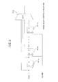
- FIG. 1 is a circuit diagram of a direct RF modulation transmitter according to this embodiment.
- the direct RF modulation transmitter according to this embodiment is an IQ quadrature amplitude modulation method type (CARTESIAN type) direct RF modulation transmitter.
- the direct RF modulation transmitter according to this embodiment includes an N-number of direct RF converters (referred to as DRCs hereafter) 302a to 302n to which an I digital baseband signal is input, and an M-number of DRCs 306a to 306m to which a Q digital baseband signal is input.
- DRCs direct RF converters
- the DRCs 302a to 302n constitute a first block of DRCs
- the DRCs 306a to 306m constitute a second block of DRCs.
- the DRCs 302a to 302n are connected to corresponding delay circuits 304a to 304n (delay circuits having the same a, b, ... n attached after the number) and constitute direct RF converters each having an input signal delaying function (referred to as DDRC (Delay-attached Direct RF Converter) hereafter) 301a to 301n.
- the DRCs 306a to 306m are connected to corresponding delay circuits 307a to 307m (delay circuits having the same a, b ... n attached after the number) and constitute DDRCs 308a to 308m.
- the direct RF modulation transmitter is constituted by a Divide-by-2 divider 303, which receives transmission local RF signals Loin+ and L oin- , and generates a pair of differential local signals T xLoI+ and T xLoI- and another pair of differential local signals T xLoQ+ and T xLoQ- differing in phase by 90 degrees, an output matching circuit 305, and a delay control circuit 309, which controls delay amount of input data to be input to the N-number of DDRCs 301 and the M-number of DDRCs 308.
- the output matching circuit 305 is a circuit having a bandpass-type gain characteristic, which has the frequency of the transmission carrier wave as a central frequency, and is constituted by passive elements, such as a capacity and/or an inductor element.
- the direct RF modulation transmitter illustrated in FIG. 1 carries out addition of output differential signals output from the DRCs 302a to 302n and the output differential signals output from the DRCs 306a to 306m by connecting signal paths on the premise that the DRCs 302a to 302n and the DRCs 306a to 306m output currents. Alternatively, it may be added by the output matching circuit 305.
- the delay control circuit 309 can set independently each of delay amounts for input data of the DDRCs 301a to 301n and the DDRCs 308a to 308m.
- the delay amounts for the input data of the DDRCs 301a to 301n are D1 D2 ... DN
- delay amounts for the input data of the DDRCs 308a to 308m are D1 D2 ... DM.
- FIG. 2 is a diagram for explaining input data to be input to a DDRC (DDRC 301a in FIG. 2 ) illustrated in FIG. 1 .
- An I digital baseband signal (referred to as 'IBB Data' in FIG. 2 ) and a sampling clock signal CLK BB are input to the DRC 301a.
- the I digital baseband signal is delayed due to a delay control signal output from the delay control circuit 309 illustrated in FIG. 1 , it is input to the DRC 302a.
- an I digital baseband signal, a sampling clock signal CLK BB , and a delay control signal are input to the DDRCs 301b to 301n illustrated in FIG. 1 , and the delayed I digital baseband signal is input to each corresponding DRC.
- a Q digital baseband signal, a sampling clock signal CLK BB , and a delay control signal are input to the DDRCs 308a to 308m illustrated in FIG. 1 , and the delayed Q digital baseband signal is input to each corresponding DRC.
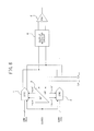
- FIG. 3 is a diagram for explaining the configuration of the delay circuit 304a illustrated in FIG. 2 .
- the delay circuit 304a is constituted by k-number of flip-flop circuits 501a to 501k, and a multiplexer 502, which has (k+1)-number of input terminals and is controlled for selection in conformity with the delay control signal output from the delay control circuit 309.
- the delay circuit 304a may set a delay amount to delay at intervals of time T clkbb of k ⁇ T clkbb from zero, namely delay the I digital baseband signal by an integral (0 to k) multiple of an arbitrary sampling clock CLK BB .
- the respective delay amounts of the input data of the DDRCs 301a to 301n illustrated in FIG. 1 are set in the following manner, for example, in conformity with the delay control signal output from the delay control circuit 309. Note that 'a' in the following equations denotes an arbitrary natural number.
- D ⁇ 1 0
- D ⁇ 2 T clkbb ⁇ a
- D ⁇ 3 2 ⁇ T clkbb ⁇ a
- DN N - 1 ⁇ T clkbb ⁇ a
- the respective delay amounts of the input data of the DDRCs 308a to 308m illustrated in FIG. 1 are set in the following manner, for example, in conformity with the delay control signal output from the delay control circuit 309.
- 'a' in the following equations denotes an arbitrary natural number.
- D ⁇ 1 0
- D ⁇ 2 T clkbb ⁇ a
- D ⁇ 3 2 ⁇ T clkbb ⁇ a
- DM M - 1 ⁇ T clkbb ⁇ a
- Quantization noise generated by the direct RF modulation transmitter illustrated in FIG. 1 will be described.
- Quantization noise generated through digital-to-analog conversion by the DDRCs 301a to 301n illustrated in FIG. 1 is affected at the output point of the direct RF modulation transmitter by a filtering effect represented by the following Equation 4 on the higher frequency wave side than the transmission carrier frequency beginning at the transmission carrier frequency.
- a filtering effect represented by the following Equation 4
- Equation 4 represents the filtering effect using a Z function with a sampling clock frequency fs as a reference.
- 'a' in Equation 4 denotes a natural number resulting from normalizing delay amount in units of the sampling clock pulse (T clkbb )
- delay of the N-th DDRC is 0, Tclkbb ⁇ a, 2 ⁇ T clkbb ⁇ a, ... n ⁇ T clkbb ⁇ a for the first to the N-th DDRC, respectively.
- f off denotes a detuning frequency from the transmission carrier frequency.
- the fact that Equation 4 represents the filtering effect can be easily and clearly explained by taking the case where the differential local signals T xLoI+ , T xLoI- , T xLoI+ and T xLoQ- with the direct RF modulation transmitter illustrated in FIG. 1 are zero as a conceptual model.
- the DRCs 302a to 302n and 306a to 306m are simple digital-to-analog converters that do not conduct frequency conversion.
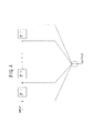
- Digital-to-analog conversion is an equivalent conversion with a gain 1, and focusing on the I digital baseband signal as illustrated in FIG. 4 , equivalent functional characteristics represented by a transfer function for Z transform may be considered.
- This is a well-known finite impulse response (FIR) filter, which clarifies that quantization noise even in the direct RF modulation transmitter is suppressed as represented in Equation 4.
- FIR finite impulse
- FIG. 5 illustrates gain characteristics for quantization noise when fs is 1 Hz, local frequency is 100 Hz, N is 2, and a is 1 as an example.
- the longitudinal axis of FIG. 5 gives gain of the direct RF modulation transmitter, and the lateral axis gives frequencies of signals.
- a frequency where gain given in the longitudinal axis is a local minimum is typically called a Notch frequency.
- Low quantization noise can be implemented near the Notch frequency by thoroughly filtering the quantization noise calculated based on the bit number in the digital-to-analog conversion.
- the Notch frequency may be arbitrarily set by combining number of stages N of the DDRCs and the sampling frequency fs. With this embodiment, adjustment of the Notch frequency to the low noise required frequency band allows control of the bit number in the digital-to-analog conversion required by the respective DRCs. Moreover, with the direct RF modulation transmitter illustrated in FIG.
- the delay control circuit 309 sets the same delay amount for the i-th (i is a number equal to or greater than 1 and equal to or less than N) DRC of the DRCs 302a to 302n and the i-th DRC of the DRCs 306a to 306m when the N-number of DRCs 302a to 302n and the M-number of DRCs 306a to 306m are the same (for the sake of simplicity of explanation, there are an N-number of the DRCs 302a to 302n and an N-number of the DRCs 306a to 306m.)
- filtering characteristics of the filtering of the quantization noise generated during the digital-to-analog conversion of the I digital baseband signal and quantization noise generated during the digital-to-analog conversion of the Q digital baseband signal are the same. Furthermore, it can be understood from the properties of the FIR filter that the filtering effect is highest at a predetermined detuning frequency.
- area of an entire current source of a direct RF modulator using conventional DRCs and area of an entire current source of a direct RF modulator constituted by the DRCs and the delay control circuit to which the present invention is applied are compared using specific numbers.
- the area of the entire current source of a 10-bit DRC in the conventional direct RF modulation transmitter is referred to as SO.
- the bit number is increased by only one bit in order to reduce the quantization noise, the area of the entire current source will be four times SO.
- the area of the entire current source will be 16 times SO.
- the noise effect as a result thereof is 6 dB and 12 dB, respectively, according to the aforementioned Equation 2.
- the area of the entire current source thereof only needs to be two times SO. Moreover, even if N and M are set to 4, it only becomes four times the original area SO.
- a low noise transmitter can be implemented with a smaller area than in the case of the above example of simply increasing the bit number of the conventional direct RF modulation transmitter.
- the entire noise floor cannot be reduced.
- the communication system strictly requires low noise in a frequency band of a predetermined range. Therefore, if the sampling frequency is adjusted using Equation 4 in accordance with the frequency band that requires low noise, number N of the DRCs can be controlled to a relatively small number.
- noise in the vicinity of the target band can be greatly reduced lower than the aforementioned 6 dB and 12 dB due to the notch illustrated in FIG. 5 .
- this allows implementation of a direct RF modulation transmitter with a smaller area and less noise than by the conventional method.
- the present invention described above is not particularly limited to the exemplary embodiments described and illustrated in detail, and includes all embodiments bringing about the same results according to the object of the present invention.
- the present invention is not limited to combination of aspects of the invention claimed in the appended claims, and may be attained by some of various desired combinations of all disclosed aspects.
- the transmitter of the present invention can have a miniaturized circuit scale with little noise, and thus is a preferable configuration for small equipment.
Landscapes
- Engineering & Computer Science (AREA)
- Physics & Mathematics (AREA)
- Computer Networks & Wireless Communication (AREA)
- Signal Processing (AREA)
- Mathematical Physics (AREA)
- Theoretical Computer Science (AREA)
- Software Systems (AREA)
- Computer Hardware Design (AREA)
- General Physics & Mathematics (AREA)
- Transmitters (AREA)
- Amplitude Modulation (AREA)
Applications Claiming Priority (2)
| Application Number | Priority Date | Filing Date | Title |
|---|---|---|---|
| JP2011125815 | 2011-06-03 | ||
| PCT/JP2012/003373 WO2012164876A1 (fr) | 2011-06-03 | 2012-05-23 | Emetteur |
Publications (2)
| Publication Number | Publication Date |
|---|---|
| EP2571175A1 true EP2571175A1 (fr) | 2013-03-20 |
| EP2571175A4 EP2571175A4 (fr) | 2014-02-19 |
Family
ID=47258753
Family Applications (1)
| Application Number | Title | Priority Date | Filing Date |
|---|---|---|---|
| EP12793290.3A Withdrawn EP2571175A4 (fr) | 2011-06-03 | 2012-05-23 | Emetteur |
Country Status (4)
| Country | Link |
|---|---|
| US (1) | US8929480B2 (fr) |
| EP (1) | EP2571175A4 (fr) |
| JP (1) | JP5416281B2 (fr) |
| WO (1) | WO2012164876A1 (fr) |
Families Citing this family (6)
| Publication number | Priority date | Publication date | Assignee | Title |
|---|---|---|---|---|
| JP2014049929A (ja) * | 2012-08-31 | 2014-03-17 | Asahi Kasei Electronics Co Ltd | 送信器 |
| JP6265206B2 (ja) * | 2013-03-07 | 2018-01-24 | 日本電気株式会社 | 無線送信装置および無線送信方法 |
| EP2905894B1 (fr) * | 2014-02-06 | 2017-05-17 | IMEC vzw | Circuit de modulation pour un dispositif radio et procédé associé |
| KR102268110B1 (ko) * | 2014-08-05 | 2021-06-22 | 삼성전자주식회사 | 데이터를 변조하는 방법 및 장치 및 기록 매체 |
| KR102155060B1 (ko) * | 2014-10-24 | 2020-09-11 | 에스케이하이닉스 주식회사 | 멀티 레벨 메모리 소자 및 그의 데이터 센싱 방법 |
| US10284202B1 (en) | 2018-04-02 | 2019-05-07 | Raytheon Company | Generating analog output from a field programmable gate array by combining scaled digital outputs |
Family Cites Families (12)
| Publication number | Priority date | Publication date | Assignee | Title |
|---|---|---|---|---|
| AU5881998A (en) | 1997-02-27 | 1998-09-18 | Matsushita Electric Industrial Co., Ltd. | Modulator and modulation method |
| US7110739B2 (en) | 2003-04-10 | 2006-09-19 | Powerwave Technologies, Inc. | Multi-transmitter communication system employing anti-phase pilot signals |
| JP2005115654A (ja) | 2003-10-08 | 2005-04-28 | Sony Corp | 情報処理装置および方法、プログラム格納媒体、並びにプログラム |
| US7421037B2 (en) * | 2003-11-20 | 2008-09-02 | Nokia Corporation | Reconfigurable transmitter with direct digital to RF modulator |
| US6980779B2 (en) | 2003-11-20 | 2005-12-27 | Nokia Corporation | RF transmitter using digital-to-RF conversion |
| US8254865B2 (en) * | 2006-04-07 | 2012-08-28 | Belair Networks | System and method for frequency offsetting of information communicated in MIMO-based wireless networks |
| JP4640454B2 (ja) * | 2008-06-24 | 2011-03-02 | ソニー株式会社 | 変調回路、変調方法、プログラム、および通信装置 |
| JP2010245962A (ja) | 2009-04-08 | 2010-10-28 | Toshiba Corp | 変調装置及び変調方法 |
| US8542773B2 (en) | 2009-12-18 | 2013-09-24 | Electronics And Telecommunications Research Institute | Digital RF converter, digital RF modulator and transmitter including the same |
| US8385469B2 (en) * | 2010-01-20 | 2013-02-26 | Panasonic Corporation | High-efficiency all-digital transmitter |
| US8767845B2 (en) * | 2010-03-02 | 2014-07-01 | The Aerospace Corporation | Increased capacity communication links with spectrum sharing |
| US20130003881A1 (en) * | 2011-06-30 | 2013-01-03 | Imec | Radio Frequency Modulators |
-
2012
- 2012-05-23 JP JP2012534475A patent/JP5416281B2/ja not_active Expired - Fee Related
- 2012-05-23 US US13/805,847 patent/US8929480B2/en not_active Expired - Fee Related
- 2012-05-23 EP EP12793290.3A patent/EP2571175A4/fr not_active Withdrawn
- 2012-05-23 WO PCT/JP2012/003373 patent/WO2012164876A1/fr not_active Ceased
Also Published As
| Publication number | Publication date |
|---|---|
| US8929480B2 (en) | 2015-01-06 |
| JP5416281B2 (ja) | 2014-02-12 |
| US20130093495A1 (en) | 2013-04-18 |
| JPWO2012164876A1 (ja) | 2015-02-23 |
| WO2012164876A1 (fr) | 2012-12-06 |
| EP2571175A4 (fr) | 2014-02-19 |
Similar Documents
| Publication | Publication Date | Title |
|---|---|---|
| EP2571175A1 (fr) | Emetteur | |
| US7091778B2 (en) | Adaptive wideband digital amplifier for linearly modulated signal amplification and transmission | |
| US6980779B2 (en) | RF transmitter using digital-to-RF conversion | |
| US8664999B2 (en) | Mixer arrangement | |
| US7812751B2 (en) | Method and device for digital-to-analog conversion with filtering | |
| US8718576B2 (en) | Radio frequency modulator and method thereof | |
| JP2008509575A (ja) | ディジタル帯域通過シグマ・デルタ変調器を含む全ディジタル送信機 | |
| CN104184452A (zh) | 数据转换装置、数字传送装置与数字转换方法 | |
| CN106688184A (zh) | 用于低毛刺噪声分段式dac的混合r‑2r结构 | |
| US7792214B2 (en) | Polar modulation transmitter circuit and communications device | |
| EP2037584A1 (fr) | Procédé pour effectuer une conversion numérique/analogique d'un signal numérique, et dispositif électronique correspondant | |
| EP1925094B1 (fr) | Modulateur de fréquence radio multibandes | |
| EP2709279A1 (fr) | Modulateur numérique | |
| EP1987593A1 (fr) | Dispositif de conversion numérique-radiofréquence, série de puces, emetteur, terminal utilisateur et procédé de traitement des données | |
| US9264076B2 (en) | Signal generation device | |
| US20150049842A1 (en) | Transmitter and transmitting method | |
| US20120231724A1 (en) | Filtering circuit with jammer generator | |
| KR101292667B1 (ko) | 디지털 rf 컨버터 및 이를 포함하는 디지털 rf 변조기와 송신기 | |
| US10044322B2 (en) | Radio frequency signal synthesizer circuit and method for generating a radio frequency signal | |
| JP2013038461A (ja) | 直接rf変調送信器、直接rf変調送信器のサンプリングクロック周波数設定方法 | |
| Kosunen | Digital signal processing and digital-to-analog converters for wide-band transmitters | |
| JP2014049929A (ja) | 送信器 | |
| JP2009284065A (ja) | 無線送信機の送信回路 |
Legal Events
| Date | Code | Title | Description |
|---|---|---|---|
| PUAI | Public reference made under article 153(3) epc to a published international application that has entered the european phase |
Free format text: ORIGINAL CODE: 0009012 |
|
| 17P | Request for examination filed |
Effective date: 20121213 |
|
| AK | Designated contracting states |
Kind code of ref document: A1 Designated state(s): AL AT BE BG CH CY CZ DE DK EE ES FI FR GB GR HR HU IE IS IT LI LT LU LV MC MK MT NL NO PL PT RO RS SE SI SK SM TR |
|
| A4 | Supplementary search report drawn up and despatched |
Effective date: 20140122 |
|
| RIC1 | Information provided on ipc code assigned before grant |
Ipc: H04B 1/04 20060101AFI20140116BHEP Ipc: H04L 27/36 20060101ALI20140116BHEP Ipc: H03D 7/00 20060101ALI20140116BHEP |
|
| DAX | Request for extension of the european patent (deleted) | ||
| GRAP | Despatch of communication of intention to grant a patent |
Free format text: ORIGINAL CODE: EPIDOSNIGR1 |
|
| INTG | Intention to grant announced |
Effective date: 20180514 |
|
| STAA | Information on the status of an ep patent application or granted ep patent |
Free format text: STATUS: THE APPLICATION IS DEEMED TO BE WITHDRAWN |
|
| 18D | Application deemed to be withdrawn |
Effective date: 20180925 |