EP2573802B1 - Matériaux poreux scellés, leurs procédés de fabrication et dispositifs semi-conducteurs les comprenant - Google Patents
Matériaux poreux scellés, leurs procédés de fabrication et dispositifs semi-conducteurs les comprenant Download PDFInfo
- Publication number
- EP2573802B1 EP2573802B1 EP12185247.9A EP12185247A EP2573802B1 EP 2573802 B1 EP2573802 B1 EP 2573802B1 EP 12185247 A EP12185247 A EP 12185247A EP 2573802 B1 EP2573802 B1 EP 2573802B1
- Authority
- EP
- European Patent Office
- Prior art keywords
- layer
- sealing
- porous material
- sealing layer
- pores
- Prior art date
- Legal status (The legal status is an assumption and is not a legal conclusion. Google has not performed a legal analysis and makes no representation as to the accuracy of the status listed.)
- Active
Links
Images





Classifications
-
- H—ELECTRICITY
- H10—SEMICONDUCTOR DEVICES; ELECTRIC SOLID-STATE DEVICES NOT OTHERWISE PROVIDED FOR
- H10P—GENERIC PROCESSES OR APPARATUS FOR THE MANUFACTURE OR TREATMENT OF DEVICES COVERED BY CLASS H10
- H10P95/00—Generic processes or apparatus for manufacture or treatments not covered by the other groups of this subclass
- H10P95/08—Planarisation of organic insulating materials
-
- H—ELECTRICITY
- H10—SEMICONDUCTOR DEVICES; ELECTRIC SOLID-STATE DEVICES NOT OTHERWISE PROVIDED FOR
- H10P—GENERIC PROCESSES OR APPARATUS FOR THE MANUFACTURE OR TREATMENT OF DEVICES COVERED BY CLASS H10
- H10P95/00—Generic processes or apparatus for manufacture or treatments not covered by the other groups of this subclass
-
- H—ELECTRICITY
- H10—SEMICONDUCTOR DEVICES; ELECTRIC SOLID-STATE DEVICES NOT OTHERWISE PROVIDED FOR
- H10P—GENERIC PROCESSES OR APPARATUS FOR THE MANUFACTURE OR TREATMENT OF DEVICES COVERED BY CLASS H10
- H10P14/00—Formation of materials, e.g. in the shape of layers or pillars
- H10P14/60—Formation of materials, e.g. in the shape of layers or pillars of insulating materials
- H10P14/65—Formation of materials, e.g. in the shape of layers or pillars of insulating materials characterised by treatments performed before or after the formation of the materials
- H10P14/6516—Formation of materials, e.g. in the shape of layers or pillars of insulating materials characterised by treatments performed before or after the formation of the materials of treatments performed after formation of the materials
- H10P14/6548—Formation of materials, e.g. in the shape of layers or pillars of insulating materials characterised by treatments performed before or after the formation of the materials of treatments performed after formation of the materials by forming intermediate materials, e.g. capping layers or diffusion barriers
-
- H—ELECTRICITY
- H10—SEMICONDUCTOR DEVICES; ELECTRIC SOLID-STATE DEVICES NOT OTHERWISE PROVIDED FOR
- H10P—GENERIC PROCESSES OR APPARATUS FOR THE MANUFACTURE OR TREATMENT OF DEVICES COVERED BY CLASS H10
- H10P14/00—Formation of materials, e.g. in the shape of layers or pillars
- H10P14/60—Formation of materials, e.g. in the shape of layers or pillars of insulating materials
- H10P14/66—Formation of materials, e.g. in the shape of layers or pillars of insulating materials characterised by the type of materials
- H10P14/665—Porous materials
-
- H—ELECTRICITY
- H10—SEMICONDUCTOR DEVICES; ELECTRIC SOLID-STATE DEVICES NOT OTHERWISE PROVIDED FOR
- H10P—GENERIC PROCESSES OR APPARATUS FOR THE MANUFACTURE OR TREATMENT OF DEVICES COVERED BY CLASS H10
- H10P14/00—Formation of materials, e.g. in the shape of layers or pillars
- H10P14/60—Formation of materials, e.g. in the shape of layers or pillars of insulating materials
- H10P14/69—Inorganic materials
- H10P14/692—Inorganic materials composed of oxides, glassy oxides or oxide-based glasses
- H10P14/6921—Inorganic materials composed of oxides, glassy oxides or oxide-based glasses containing silicon
- H10P14/6922—Inorganic materials composed of oxides, glassy oxides or oxide-based glasses containing silicon the material containing Si, O and at least one of H, N, C, F or other non-metal elements, e.g. SiOC, SiOC:H or SiONC
-
- Y—GENERAL TAGGING OF NEW TECHNOLOGICAL DEVELOPMENTS; GENERAL TAGGING OF CROSS-SECTIONAL TECHNOLOGIES SPANNING OVER SEVERAL SECTIONS OF THE IPC; TECHNICAL SUBJECTS COVERED BY FORMER USPC CROSS-REFERENCE ART COLLECTIONS [XRACs] AND DIGESTS
- Y10—TECHNICAL SUBJECTS COVERED BY FORMER USPC
- Y10T—TECHNICAL SUBJECTS COVERED BY FORMER US CLASSIFICATION
- Y10T428/00—Stock material or miscellaneous articles
- Y10T428/249921—Web or sheet containing structurally defined element or component
- Y10T428/249953—Composite having voids in a component [e.g., porous, cellular, etc.]
- Y10T428/249978—Voids specified as micro
-
- Y—GENERAL TAGGING OF NEW TECHNOLOGICAL DEVELOPMENTS; GENERAL TAGGING OF CROSS-SECTIONAL TECHNOLOGIES SPANNING OVER SEVERAL SECTIONS OF THE IPC; TECHNICAL SUBJECTS COVERED BY FORMER USPC CROSS-REFERENCE ART COLLECTIONS [XRACs] AND DIGESTS
- Y10—TECHNICAL SUBJECTS COVERED BY FORMER USPC
- Y10T—TECHNICAL SUBJECTS COVERED BY FORMER US CLASSIFICATION
- Y10T428/00—Stock material or miscellaneous articles
- Y10T428/249921—Web or sheet containing structurally defined element or component
- Y10T428/249953—Composite having voids in a component [e.g., porous, cellular, etc.]
- Y10T428/249978—Voids specified as micro
- Y10T428/249979—Specified thickness of void-containing component [absolute or relative] or numerical cell dimension
-
- Y—GENERAL TAGGING OF NEW TECHNOLOGICAL DEVELOPMENTS; GENERAL TAGGING OF CROSS-SECTIONAL TECHNOLOGIES SPANNING OVER SEVERAL SECTIONS OF THE IPC; TECHNICAL SUBJECTS COVERED BY FORMER USPC CROSS-REFERENCE ART COLLECTIONS [XRACs] AND DIGESTS
- Y10—TECHNICAL SUBJECTS COVERED BY FORMER USPC
- Y10T—TECHNICAL SUBJECTS COVERED BY FORMER US CLASSIFICATION
- Y10T428/00—Stock material or miscellaneous articles
- Y10T428/249921—Web or sheet containing structurally defined element or component
- Y10T428/249953—Composite having voids in a component [e.g., porous, cellular, etc.]
- Y10T428/249981—Plural void-containing components
Definitions
- the present invention relates to methods for sealing a porous material. More specifically the present invention relates to the field of sealing porous low-k materials for semiconductor manufacturing. The present invention further relates to sealed porous materials, in particular sealed porous low-k dielectric materials. The present invention also relates to semiconductor devices comprising sealed porous materials, in particular sealed porous low-k dielectric materials.
- the manufacturing of various electronic devices now requires the cost-effective production of very small structures and features, e.g., structures and features having a characteristic dimension at the micrometer or nanometer size scale.
- This manufacturing includes the formation of electrically conductive material(s) (e.g., aluminum, copper, etc.) and electrically insulating dielectric material(s) (e.g., silicon dioxide, silicon nitride, etc.) on or as part of a substrate.
- the electrically conductive material(s) are typically separated by regions of dielectric material(s) so as to define electrical elements (e.g., transistors, capacitors, etc.) and interconnections between such electrical elements.
- interconnect layer(s) Each interconnect layer comprises conductive material(s) separated by dielectric material(s).
- a first layer of dielectric material is formed on an electrically conductive material (first conductive layer).
- a second layer of dielectric material is formed on the first layer of dielectric material.
- Trenches e.g. lines
- vias e.g., holes
- Electrically conductive material is subsequently formed in the trenches and vias so as to electrically connect the now electrically conductive trenches (second conductive layer) to the electrically conductive material (first conductive layer) through the now electrically conductive vias.
- High performance microelectronic devices are obtained by the continuous downscaling of their critical dimensions.
- this downscaling also leads to an increase in RC-delay and cross talk which adversely affects the performance of the device.
- the dielectric constant of the low k-material that insulates the interconnect wiring has to decrease.
- the decrease in dielectric constant will also lead to a lower power consumption of the device.
- a key factor to decrease the k-value drastically is introducing porosity into the electrically insulating dielectric material because air has a dielectric constant of 1 which is the lowest value that can be obtained.
- pore sealing technologies are essential for the implementation of mesoporous structures as low-k materials.
- a known sealing method is a plasma treatment of the porous low-k material which creates a densification at the surface of the low-k material.
- plasma treatments can also cause a change in structure, composition and porosity of the material.
- mesoporous films are sensitive for diffusion of reactive components which means that plasma treatment might affect the quality of the bulk porous material as well.
- a known alternative is the deposition of a dense layer via chemical vapor deposition (CVD) or atomic layer deposition (ALD). Pore sizes smaller than 2 nm can be sealed by plasma treatment, CVD and ALD.
- CVD chemical vapor deposition
- ALD atomic layer deposition
- Several drawbacks of these techniques are the diffusion of the barrier into the pores and the fact that current dielectric barriers have a relatively high dielectric constant.
- Molecular self-assembly is a technique that can be used to produce very small structures having a dimension at the nanometer size scales.
- Molecular self-assembly can be used to produce a variety of material formations, such as molecular monolayers (often referred to as self-assembled monolayers, or SAMs), molecular multilayers and nanostructures (e.g., nanotubes, nanowires).
- SAMs molecular monolayers
- molecular multilayers e.g., nanotubes, nanowires
- a SAM has been used as a barrier layer (replacing the deposited barrier layer) that inhibits diffusion of copper into a dielectric material.
- this SAM inhibits copper diffusion into SiO2 or fluorinated SiO2, both of which are non-porous dielectric materials.
- Porous dielectric materials provide additional challenges to inhibiting diffusion because the pores of porous dielectric materials provide another diffusion pathway for foreign material (e.g., barrier layer material, copper) into the dielectric material.
- SAMs have been proposed for use as bulk diffusion barrier layers, especially for use with dense dielectric materials such as silicon dioxide. There is a need in the art for preventing diffusion of foreign material through the exposed pores of porous dielectrics.
- the dielectric constant of the interlayer dielectrics must be smaller than 2.0.
- ultra low-k materials generally have a porosity exceeding 50% and a pore size of 3 nm or more.
- the existing sealing technologies are no longer efficient.
- Pieces of prior art relevant to the present disclosure are e.g. WO 01/15214 A1 (ALLIED SIGNAL INC [US]) 1 March 2001 (2001-03-01), and US 2005/020074 A1 (KLOSTER GRANT [US] ET AL) 27 January 2005 (2005-01-27).
- the present invention relates to a method as defined in claim 1, i.e. a method for at least partially sealing a porous material or layer, said method comprising:
- the method may further comprise, after forming the sealing layer, the step of performing a thermal treatment, for instance by submitting the combination of the porous layer and the sealing, layer to heat.
- the porous material may be a low-k or ultra low-k dielectric material, for instance a dielectric material with a k value from about 1.8 to 3.6.
- the porous material may comprise pores having a dimension (e.g. a diameter) larger than 2 nm, or at least 3 nm, and up to 50 nm, for instance up to 25 nm.
- the sealing compound may be applied by a spin-on technique.
- the precursor solution comprising cyclic carbon bridged organosilica and/or bridged organosilanes may further comprise water, an acid, and/or a solvent, each of them being as described in more details below.
- the concentration of carbon bridged organosilica and/or bridged organosilanes and the ageing conditions may be selected to obtain a sealing compound having a viscosity between 1 and 3 cP (centipoises).
- ageing of the precursor solution may be performed for an ageing time of at least 12 hours, and up to about 200 hours, depending upon parameters such as, but not limited to, the ageing temperature, the concentration of the carbon bridged organosilica and/or the bridged organosilane in the solvent(s) and so on .
- the method may further comprise applying one or more post-treatment steps after forming the sealing layer onto the porous material.
- one post-treatment step may be a step having the effect of making the sealing layer more hydrophobic in order to improve the sealing power, e.g. completely sealing or blocking the pores of the sealing layer.
- one post-treatment step may be performed by exposing the assembly of layers obtained after forming the sealing layer (3) to an end-capping compound comprising hydrophobic groups such as hexamethyldisilazane (HDMS- or trimethylsilane (TMS) or any other silanol end-capping compound comprising hydrophobic groups as detailed below, e.g. a chlorotrialkylsilane.
- an end-capping compound comprising hydrophobic groups such as hexamethyldisilazane (HDMS- or trimethylsilane (TMS) or any other silanol end-capping compound comprising hydrophobic groups as detailed below, e.g. a chlorotrialkylsilane.
- one post-treatment may be selected to create functional groups on the surface of the sealing layer, e.g. grafting, prior to another process step.
- a subsequent process step may be an Atomic Layer Deposition step, and the functional groups created by such step may be hydroxyl (OH) groups.
- the present invention relates to an at least partially sealed porous material or layer layer comprising:
- the present invention may also relate to an at least partially sealed porous layer comprising:
- the sealing layer may have a k value comprised between about 1.8 and 3.6, for instance comprised between about 2.8 and 3.5, or comprised between about 1.8 and 2.2.
- the present invention describes a method for pore sealing of a porous layer by applying a sealing solution comprising oligomers to form a sealing layer. Additionally the method can comprise a thermal treatment applied after forming the sealing layer.
- the porous layer may comprise/consist a mesoporous material, i.e. a material containing pores with diameters between 2 and 50 nm.
- the porous layer may comprise/consist a low-k dielectric material such as currently used in semiconductor manufacturing.
- the sealing layer formed comprises pores having a diameter not above 0.6 nm, for instance from 0.1 to 0.6 nm.
- a sealing layer is suitable to be used in semiconductor manufacturing as a protective layer of the low-k material (e.g. low-k mesoporous material) during the further process steps (e.g. barrier deposition such as a copper barrier or a barrier of another electrically conductive material).
- a third aspect of the present invention relates to a semiconductor device comprising an at least partially sealed porous material or layer as described in any one of the above embodiments of the second aspect of the present invention, or an at least partially sealed porous material or layer obtained by a method as described in any one of the above embodiments of the first aspect of the present invention.
- the semiconductor device of the third aspect of the present invention may further a copper barrier or a barrier of another electrically conductive material.
- Copper is commonly used as the electrically conductive material in electronic devices. Copper can be used to fill trenches and/or vias (or other, similar features) of an electronic device.
- a description of a method for forming a copper interconnection between electrical elements formed in or on a substrate (e.g. semiconductor) follows. The formation of a copper interconnection etches a structure (e.g., trenches and/or vias) in a dielectric material (e.g., silicon dioxide). A barrier layer (e.g., tantalum and/or tantalum nitride) is formed on the dielectric material.
- a barrier layer e.g., tantalum and/or tantalum nitride
- the barrier layer prevents diffusion of copper into the dielectric material.
- the barrier layer should also adhere well to the dielectric material and to the copper subsequently formed on the barrier layer.
- a seed layer of copper is formed on the barrier layer. Copper is then formed to fill the trench or via using a bulk formation process (e.g., an electrochemical deposition process).
- the formation of copper interconnects includes two copper formation steps and because copper formed using the bulk copper formation process does not nucleate and/or adhere well on the formed barrier layer. This necessitates the formation of a copper seed layer, using a process other than a bulk formation process, on which the bulk copper does nucleate and/or adhere, for example, by providing an electrochemically reactive layer for subsequent electrochemical deposition of copper.
- the two copper formation steps are used because the copper seed layer formation step by itself (e.g., physical vapor deposition, sputtering) does not adequately fill the vias and trenches because of non-conformal step coverage produced by the physical vapor deposition process (e.g., breadloafing or excessive overhang of deposited material at the top of a trench, via or other feature).
- the copper seed layer formation step by itself e.g., physical vapor deposition, sputtering
- non-conformal step coverage produced by the physical vapor deposition process e.g., breadloafing or excessive overhang of deposited material at the top of a trench, via or other feature.
- the seed layer can be a material (e.g. ruthenium, platinum, etc.) other than copper on which copper formed using the bulk copper formation process does nucleate and/or adhere well (e.g., electrochemical deposition).
- the barrier layer formed can be a material like ruthenium on which copper can be satisfactorily formed (e.g. with good nucleation and/or adhesion) during the bulk formation so as to eliminate the need for the copper seed layer.
- the sealing layer is compatible with semiconductor manufacturing, preferably does not substantially penetrates the pore structure of the porous material underneath (e.g. low-k mesoporous material) and can be coated as thin as several nanometers.
- An additional advantage is the low dielectric constant of the sealing layer.
- Some mbodiments of the present invention describe performing additionally a post-treatment step after the sealing layer has been formed and eventually after the sealing layer has been thermally treated to form a complete hydrophobic sealed surface.
- the method discloses applying (e.g. by spin coating) of a sealing compound comprising oligomers on a porous material.
- the porous material can be formed on a substrate.
- the sealing layer formed with the method of the present invention may have a k value of about 2.8 to 3.6 both in the as-deposited, as well as in the thermally treated (baked) form, being itself a low-k material and thus perfectly compatible with semiconductor manufacturing and facilitating therefore the process integration.
- An additional advantage is that it can be spin coated, a simple and cost-effective deposition method that can be performed under ambient atmosphere.
- the sealing layer of the present invention may have a thickness in the range of several nanometers, for instance lower than 10 nm. However, depending on the semiconductor application type, thicker layers up to tens of nanometers may be deposited if required.
- a method for at least partially sealing a porous material comprising forming a sealing layer onto the porous material by applying a sealing solution comprising oligomers wherein the sealing solution is formed by ageing a precursor solution comprising silacyclohexanes.
- the at least partially sealing referred to in the various embodiments of the present invention is a sealing process whereby the sealing layer does not penetrate the pores of the porous material and whereby the sealing layer comprises narrow pores suitable to protect the porous material in different situations.
- One of these applications is semiconductor manufacturing wherein such a sealing layer protects the low-k material (porous material) during the subsequent manufacturing steps (e.g. barrier deposition).
- a substantially complete sealing can be achieved, whereby the narrow pores of the sealing layer are blocked by functional groups.
- the cyclic carbon bridged organosilica are trisilacyclohexanes such as [SiCH 2 (OEt) 2 ] 3 , [SiCH 2 ] 3 (OEt) 5 CH2Si(OEt) 3 and combinations or mixtures thereof.
- the porous material is a low-k dielectric material.
- a low-k dielectric material is a dielectric material having a dielectric constant lower than the dielectric constant of silicon dioxide (3.9).
- the low-k material can be deposited by spin-on techniques or chemical vapor deposition (CVD) techniques.
- the porous material comprises pores having a dimension larger than 0.6 nm, preferably larger than 2 nm and more preferably at least 3 nm. Porous materials with a pore dimension larger than 2 nm and up to 50 nm are also referred to as mesoporous materials in the art.
- the sealing layer is formed by coating/depositing of the sealing solution onto the porous material.
- the oligomer formation prior to coating (deposition) prevents its diffusion into the open pore structure.
- the sealing layer is dried at temperatures below 200°C in air or baked at a higher temperature in an inert atmosphere (e.g. nitrogen, argon and the like).
- the sealing solution is a liquid characterized by a certain viscosity.
- the sealing solution can be applied by spin-on techniques.
- the sealing solution can be applied by dip-coating or inkjet printing.
- the latter has the advantage of a local coating/deposition.
- the sealing solution is formed by ageing a precursor solution comprising cyclic carbon bridged organosilica and/or bridged organosilanes as precursors.
- precursors may be synthesized according to a method described by Goethals et al. in J. Mater. Chem. (2010) 20:1709 - 1716 .
- Figure 1 illustrates schematically the oligomer formation from cyclic carbon bridged organosilane precursors in an embodiment of the present invention.
- the concentrations of the precursors as well as the ageing conditions (time and temperature) are preferably selected such that the viscosity of the sealing solution is about 1.0 to 3.0 cP (mPa.s) at the temperature of coating (e.g. at room temperature, 20°C).
- the precursor solution may comprise water, an acid and/or a solvent.
- the acid catalyzes the hydrolysis and it should be miscible with the solvent.
- an acid is selected so that is volatile below 100°C under atmospheric pressure.
- the acid may be an inorganic acid such as , but not limited to, hydrochloric acid, or an organic acid.
- the solvent may be suitably selected such that it is volatile below 100°C under atmospheric pressure and miscible with water and the acid selected.
- the solvent can be an organic solvent such as, but not limited to, an alcohol or a ketone or a mixture thereof wherein the precursors are soluble.
- the solvent may be ethanol.
- the concentration of acid and the amount of water may be selected such that the precursors do not polymerize under the current ageing conditions.
- the concentration of acid and the amount of water may be selected such that the precursors do not form insoluble polymers under the ageing conditions.
- the concentration of acid and the amount of water may be selected in such a way that only soluble polymers and oligomers are formed.
- oligomers are formed.
- the porous material (2) can be formed on a substrate (1).
- the substrate is made of any material compatible with semiconductor manufacturing, such as but not limited to a silicon wafer.
- the substrate can be made of any material, a metal, an insulator a semiconductor, plastics etc.
- the sealing layer formed with the method of the present invention is also a porous material, however the pores dimension of the sealing layer are usually below about 0.6 nm, which makes it suitable for use as a protective layer for a (meso)porous material in different electronic applications.
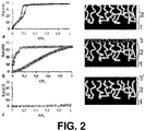
- the pores of the sealing layer having a dimension below 0.6nm are also referred to as narrow pores. This is illustrated by the schematically represented stack in Figure 2 (b, right), wherein the sealing layer (3) is shown on top of a porous material (2) formed on a substrate (1).
- the ageing conditions of the precursor solution can be varied from about 12 hours to about 1 week or 200 hours at room temperature (about 20°C). However by increasing the temperature to values higher than the room temperature but lower than the boiling point of the solvent (e.g. 78°C for ethanol) the ageing time can be reduced to about 90 minutes or even below. Specific non-limiting examples are herein further disclosed.
- the method further comprises, after forming the sealing layer, performing a thermal treatment (also referred to as bake/baking step).
- the thermal treatment can be performed at temperatures below 200°C in air or at higher temperature (up to 600°C) in inert atmosphere.
- the sealing layer can be dried at room temperature in air.
- the volatiles in the sealing layer are removed and the condensation of the cyclic carbon bridged organosilane is complete. Complete condensation means that remaining free silanol groups, present in the layer, will form Si-O-Si bonds when they are close enough for reaction.
- the method may further comprise a post-treatment applied after forming and drying/baking the sealing layer.
- the post-treatment applied may make the sealing layer hydrophobic thereby blocking the narrow pores of the sealing layer to achieve a complete sealing of the porous material underneath.
- FIG 2 c, right
- the post-treated sealing layer (3') is shown on top of a porous material (2) formed on a substrate (1).
- the post-treatment for making the sealing layer hydrophobic may be performed with a silanol end-capping compound comprising hydrophobic groups.
- said silanol end-capping compound comprising hydrophobic groups may be suitable for silylation of silanol.
- said silanol end-capping compound comprising hydrophobic groups may be suitable for trialkylsilylation (e.g. trimethylsilylation) of silanol.
- a first illustrative group of suitable silanol end-capping compounds comprising hydrophobic groups are compounds of the structural formula R n SiX 4-n wherein
- Examples of compounds belonging to this first illustrative group include, but are not limited to, trimethylchlorosilane, bromotrimethylsilane, iodotrimethylsilane, trimethylsilyl trifluoromethanesulfonate, trimethylsilyl cyanide, dimethylaminotrimethylsilane, triethylchlorosilane, isopropyldimethylchlorosilane, triisopropylchlorosilane, tert-butyldiphenylchlorosilane, phenyldimethylchlorosilane, diphenyltetramethyldisilazane, dimethyldichlorosilane, diethyldichlorosilane, tretraorthosilane, and methyltriethoxysilane.
- a second illustrative group of suitable silanol end-capping compounds comprising hydrophobic groups are compounds represented by the structural formula R' 3 SiR"SiR' 3 wherein R" is a C 1-4 alkylene (e.g. methylene or ethylene) or an arylene (e.g. phenylene) divalent group and wherein each R' is independently selected from C 1-4 alkyl (e.g. methyl, ethyl, isopropyl or tert-butyl) and C 1-4 alkoxy (e.g. methoxy or ethoxy) groups.
- R' 3 SiR"SiR' 3 wherein R" is a C 1-4 alkylene (e.g. methylene or ethylene) or an arylene (e.g. phenylene) divalent group and wherein each R' is independently selected from C 1-4 alkyl (e.g. methyl, ethyl, isopropyl or tert-butyl) and
- Examples of compounds belonging to this second illustrative group include, but are not limited to, 1,2-bis(triethoxysilyl)ethane; 1,2-bis(triethoxysilyl)methane; 1,2-bis(triethoxysilyl)benzene; and 1,2-bis(trimethoxysilyl)ethane)[F1].
- a third illustrative group of suitable silanol end-capping compounds comprising hydrophobic groups are compounds of the structural formula R 3 Si-NH-SiR 3 or cyclic compounds of the structural formula[SiR 2 NH] 3 wherein each R is as defined above.
- Examples of compounds belonging to this third illustrative group include, but are not limited to, hexamethyldisilazane, diphenyltetramethyldisilazane, and hexamethylcyclotrisilazane.
- a fourth illustrative group of suitable silanol end-capping compounds comprising hydrophobic groups are cyclic carbon bridged organosilica as defined for the precursor solution of any embodiment of the present invention.
- hydrophobic group relates to groups able to increase the hydrophobicity of a given substrate and in particular of a SiO 2 substrate.
- hydrophobic groups can be hydrocarbon groups (e.g. alkyl groups) or halocarbon groups.
- the post-treatment for making the sealing layer hydrophobic may be performed with hexamethyl disilazane (HDMS), trimethyl silane (TMS), chlorotrialkyl silanes or any equivalent thereof .
- HDMS hexamethyl disilazane
- TMS trimethyl silane
- chlorotrialkyl silanes or any equivalent thereof .
- the thermal treatment and/or the post-treatment may be selected to create functional groups on the surface of the sealing layer prior to a subsequent process step.
- functional groups are the OH groups formed before an Atomic Layer Deposition (ALD) process step, such as ALD barrier deposition on a sealed porous material.
- ALD Atomic Layer Deposition
- Such OH groups can also for instance be present at the surface of the sealing layer as the result of the non-performance of a thermal treatment after formation of the sealing layer.
- the performance of a thermal treatment will typically diminish the amount of OH groups present. In general, a longer thermal treatment and/or a thermal treatment at a higher temperature will lead to less OH groups present.
- the sealing layer (b) of said partially sealed porous material or layer may have a dielectric constant (k value) comprised between 1.8 and 3.6, for instance between 2.8 and 3.6, or between 3.0 and 3.4, both in the as-deposited as well as thermally treated (baked) or post-treated form.
- k value dielectric constant
- these values are comparable with other low-k materials and much lower than the k value of the state of the art sealing materials, which makes it suitable for protecting low-k material with large pores in semiconductor devices manufacturing.
- the sealing layer (b) of said partially sealed porous material or layer of the present invention may further comprise functional groups, preferably hydrophobic moieties, which are able to more completely block the pores of the sealing layer, thereby completely sealing the porous material of the first layer (a).
- the functional groups or hydrophobic moieties capable of blocking the pores may be obtainable by end-capping silanol groups on the sealing material by using silanol end-capping compounds comprising hydrophobic groups as defined in more specific details in any one of the previous embodiments of the first aspect of the present invention, in particular the four illustrative groups thereof.
- a semiconductor device comprising an at least partially sealed porous material or layer as defined in the second aspect of the present invention, including any one of the previous specific embodiments thereof, or an at least partially sealed porous material or layer as obtained from the method defined in the first aspect of the present invention, including any one of the previous specific embodiments thereof.
- the semiconductor device usually comprises one or more further layers of electrical elements and/or interconnections (e.g. interconnect layer(s)), each interconnect layer comprising conductive material(s) separated by dielectric material(s).
- the semiconductor device according to the third aspect of the present invention further comprises a layer of an electrically conductive material such as, but not limited to, copper.
- a semiconductor device may alternatively or further comprise a layer of a metal compound selected from the group consisting of the carbides, carbonitrides, nitrides, siliconitrides and oxynitrides of a metal selected from the group consisting of aluminium, ruthenium, tantalum, hafnium, titanium, molybdenum and tungsten, for instance tantalum nitride.
- a metal compound selected from the group consisting of the carbides, carbonitrides, nitrides, siliconitrides and oxynitrides of a metal selected from the group consisting of aluminium, ruthenium, tantalum, hafnium, titanium, molybdenum and tungsten, for instance tantalum nitride.
- the choice of the electrically conductive material or the metal compound is usually dictated by one or more of the desirable characteristics, in particular electric behavior, of the semiconductor device .
- a mesoporous silica material with an average pore diameter of 3.5 nm and a thickness of 80 nm was prepared as (meso)porous thin film material.
- the total and open porosity of the mesoporous film is shown in Table 1 and was determined with spectroscopic ellipsometry and ellipsometric porosimetry (using toluene as adsorbent) respectively.
- the open porosity refers to the volume of the pores (as percentage of the total volume of the porous material) which are accessible for toluene, while the total porosity refers to the volume of the pores (as percentage of the total volume of the porous material) which are both accessible and not accessible for toluene.
- BrijTM 76 a polyoxyethylene stearyl ether porogen template [F2]
- F3 20 ml ethanol [F3]
- 0.5 ml (0.1M) HCl 20 ml ethanol [F3]
- 1 ml of tetraethylorthosilicate (TEOS) and 0.5 ml H 2 O were added to the solution followed by aging the solution for 1 day.
- the solution was then spin coated on a Si-wafer at a rate of 5000 rpm.
- the porogen template was removed by treating the film at 400 °C for 5h.
- Pentane was added to the residue and this mixture was also filtered.
- the remaining oil consisted of cyclic carbon-bridged organosilanes of formula [SiCH 2 (OEt) 2 ] 3 and [SiCH 2 ] 3 (OEt) 5 CH 2 Si(OEt) 3 .
- a sealing compound (solution) was prepared by ageing a precursor solution comprising cyclic carbon bridged organosilane precursors, water, hydrochloric acid and ethanol. This solution was aged for one week to allow oligomer formation as schematically illustrated in Figure 1 .
- the solution comprising the oligomers was spin coated at 5000 rpm on the mesoporous silica film to form an organosilica dense top layer.
- An additional baking step (thermal treatment) was performed at 400 °C under nitrogen atmosphere to remove all the volatiles and to complete the condensation of the cyclic carbon bridged precursor.
- 0.5 ml of the cyclic carbon-bridged organosilane mixture was dissolved in the 20 ml ethanol, 0.5 ml (0.1M) HCl and 0.5 ml H 2 O and aged for 1 week. The solution was then spin coated at 5000 rpm on top of the mesoporous silica film to form an organosilica sealing layer.
- An additional baking step was performed at 400 °C under nitrogen atmosphere to remove all the volatiles and to complete the condensation of the cyclic carbon bridged precursor.
- concentrations of the cyclic carbon-bridged organosilane mixture were tested between 0.25ml to 5 ml precursor mixture for 20ml ethanol.
- Ageing conditions were also varied from 12h to 1 week at room temperature and for 90min with reflux at high temperature (immediately below the boiling temperature of ethanol) to enhance oligomer formation.
- HMDS hexamethyl disilazane
- the vacuum dried film was exposed to HMDS vapor for 2h at 130 °C and rinsed with pentane to remove unreacted HMDS.
- the refractive index and thickness of the layer was analyzed on a Woollam spectroscopic ellipsometer SentechTM 801. This non destructive method measures the change in polarization of the reflected light off a sample. By using a mathematical model, the thickness and refractive index were calculated.
- n 2 ⁇ 1 n 2 + 2 V p n p 2 ⁇ 1 n p 2 + 2 + 1 ⁇ V p n s 2 ⁇ 1 n s 2 + 2
- a spectroscopic ellipsometer SentechTM 801 at 70° incidence angle is mounted in a vacuum chamber that can be filled with solvent vapor (toluene) in a controlled way.
- solvent vapor toluene
- the pressure of the toluene vapors is raised in steps from the vacuum level up to the saturation pressure.
- the pressure dependent condensation occurs in the open pores and the refractive index of the sample is changed.
- the total pore volume is calculated from the change in refractive index using following equation.
- P n rf 2 ⁇ 1 n rf 2 + 2 ⁇ n re 2 ⁇ 1 n re 2 + 2 / n ads 2 ⁇ 1 n ads 2 + 2
- P is the porosity
- n re the refractive index of the film with empty pores
- n rf the refractive index of the film with filled pores
- n ads the refractive index of the solvent.
- Figure 2 shows the toluene adsorption/desorption isotherms (left) of the schematically represented stacks (right): (a) porous material (2) on a substrate (1); (b) sealing layer according to the method of the invention (3) on the porous material (2) on a substrate (1); (c) post-treated (HDMS) sealing layer according to the method of the invention (3') on the porous material (2) on a substrate (1).
- O.p. stands for " Open porosity " .
- the isotherm of the sample after the organosilica layer deposition and baking shows a gradually increase in toluene adsorption instead of a steep capillary condensation step. This can be assigned to the fact that toluene cannot easily diffuse into the pores which is also confirmed by the delayed desorption of the toluene.
- These isotherms are typical for porous material containing cavities. Although the open porosity is still equal to the total porosity, the pore entrances are very narrow.
- the sealing layer comprises very narrow pores (lower than or equal to 0.6nm since toluene is still admitted) which makes the sealing layer a suitable protective layer for various porous materials having larger pores, such as mesoporous materials.
- Table 1 Physical properties of the mesoporous silica film as deposited (sample 1), after sealing layer deposition and baking (sample 2) and after HDMS treatment of sample 2 (sample 3). Sample Thickne ss (nm) P tot (v%) P open (v%) P closed (v%) Contact angle (°) (1) 80 38 38 0 57 (2) 100 34 34 0 70 (3) 100 34 2.5 31.5 86
- the water contact angle increased after the HMDS treatment at about 86°.
- a highly hydrophobic surface of the sealed film was obtained, in this way preventing subsequent moisture adsorption which can lead to degradation of the k-value.
- the sealed porous material was characterized by Diffuse reflectance Fourier transform infrared spectroscopy (DRIFT) and the spectra are shown in figure 3 .
- DRIFT spectra were obtained on a NicoletTM 6700 FT-IR from Thermo Scientific.
- the thickness of the deposited sealing layer is only 20 nm, the typical peaks of the carbon-hydrogen stretch vibrations around 2900 cm -1 are not well resolved.
- BrijTM-76 (a polyoxyethylene stearyl ether porogen template) was dissolved in 20 ml ethanol and 1.5 ml (0.1M) HCl. Then, 3 ml of 1,2-bis(triethoxysilyl)ethane and 1.5 ml H 2 O were added to the solution and this was aged for 1 day. The solution was then spin coated on a Si-wafer at a rate of 5000 rpm. The porogen was removed by treating the film at 400°C for 5 hours. The higher contact angle is due to the organic components in the matrix compared to the pure mesoporous silica film of example 1.
- the sealing layer was deposited on top of the porous silica and the total thickness (porous silica + top layer) was determined.
- the thickness of the top layer can be calculated.
- a 2 layer Cauchy model was used. One layer model fits the porous film and the other the top film. Assuming that the thickness of the porous film does not change significantly after the top layer deposition, this parameter can be fixed and only the parameters that influence the refractive index are fitted. In the case that the refractive index of the porous film is similar before and after the top layer deposition, there is no significant diffusion of the top layer.
- the prepared precursor solution of example 2 (not yet aged) was boiled to evaporate ethanol until the solution color changed from transparent to yellow and a high viscous liquid was obtained, indicating that condensation reactions took place (common sol-gel chemistry).
- the highly viscous liquid was boiled for an additional 10 minutes.
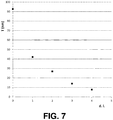
- ethanol was added again to obtain the original solution volume (dilution level d.1. 0) and the solution was further diluted (10, 100, 1000, or 10000 times corresponding to a dilution level of 1, 2, 3 and 4 respectively) with ethanol to control the thickness (T) of the layer and speed-up oligomer formation.
- the influence of the ethanol concentration on the thickness (T) is shown in figure 7 .
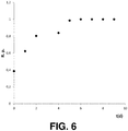
- the thickness of the layer is more or less divided by two. Further, confirmation of the oligomer formation is that at dilution level 0, the thickness of the sealant layer is much higher than when the pristine starting solution is deposited (90 vs 20-40 nm). Also with this dilution approach very thin layers can be obtained ( ⁇ 10 nm) To investigate if the ageing time needed to avoid diffusion is decreased with this method. The level 1 diluted solution was deposited on a porous silica material and the remaining porosity of this layer was determined with ellipsometry.
- a fourth illustrative group of suitable silanol end-capping compounds comprising hydrophobic groups are cyclic carbon bridged organosilica as defined for the precursor solution of any embodiment of the present invention.
- grafting was applied on mesoporous silica powder, the material was characterized with FTIR spectroscopy.
- the FTIR spectrum in figure 9 shows a typical spectrum for silica materials. At 1150 cm -1 the Si-O-Si peak is clearly visible and the peak at 3750 cm -1 can be assigned to the free silanol groups.
- the end-capping follows the reaction given in Figure 10 .
- the silanols of the material react with the Si centers of the silane precursor and ethanol comes free.
Landscapes
- Internal Circuitry In Semiconductor Integrated Circuit Devices (AREA)
- Formation Of Insulating Films (AREA)
Claims (13)
- Procédé pour rendre au moins partiellement étanche un matériau ou une couche poreux(-euse) (2) comprenant :- la fourniture d'un matériau poreux (2),- la formation d'une couche d'étanchéité (3) sur le matériau ou la couche poreux (-euse) (2) en appliquant un composé d'étanchéité comprenant des oligomères,caractérisé en ce que les oligomères sont formés en vieillissant une solution de précurseur comprenant des trisilacyclohexanes tels que [SiCH2(OEt)2]3, [SiCH2]3(OEt)5CH2Si(OEt)3 et des combinaisons ou mélanges de ceux-ci en toute proportion.
- Procédé selon la revendication 1, dans lequel le matériau poreux (2) est un matériau diélectrique à faible k.
- Procédé selon l'une quelconque des revendications 1 à 2, comprenant en outre la soumission à un traitement thermique de l'ensemble de couches obtenu après la formation de la couche d'étanchéité (3).
- Procédé selon l'une quelconque des revendications 1 à 3, dans lequel le matériau poreux (2) comprend des pores ayant une dimension allant de 2 nm à 50 nm.
- Procédé selon l'une quelconque des revendications 1 à 4, dans lequel le composé d'étanchéité est appliqué à l'aide d'une technique de dépôt par rotation.
- Procédé selon l'une quelconque des revendications 1 à 5, dans lequel la solution de précurseur comprend en outre de l'eau et/ou un acide et/ou un solvant.
- Procédé selon l'une quelconque des revendications 1 à 6, dans lequel le composé d'étanchéité comprenant des oligomères manifeste une viscosité valant entre 1 et 3 mPa·s.
- Procédé selon l'une quelconque des revendications 1 à 7, dans lequel le vieillissement est exécuté pendant une période de vieillissement d'au moins 90 minutes.
- Procédé selon l'une quelconque des revendications 1 à 8, comprenant en outre le post-traitement de l'ensemble de couches obtenu après la formation de la couche d'étanchéité (3), ledit post-traitement rendant la couche d'étanchéité (3) plus hydrophobe.
- Procédé selon la revendication 9, dans lequel le post-traitement comprend l'exposition de l'ensemble de couches obtenu après la formation de la couche d'étanchéité (3) à un composé de coiffage d'extrémité comprenant des groupes hydrophobes.
- Procédé selon la revendication 10, dans lequel ledit composé de coiffage d'extrémité comprenant des groupes hydrophobes est sélectionné à partir du groupe constitué par :- des composés de la formule structurelle RnSiX4-n dans laquelle n vaut de 1 à 3 lorsque X n'est pas OR' et dans laquelle n vaut de 0 à 3 lorsque X est OR', chaque R est indépendamment sélectionné à partir de groupes hydrocarbyle saturés et de groupes hydrocarbyle aromatiques, et chaque X est indépendamment un groupe qui convient à une réaction avec un groupe silanol ;- des composés représentés par la formule structurelle R'3SiR"SiR'3 dans laquelle R" est un alkylène en C1-4 ou un groupe arylène divalent et dans laquelle chaque R' est indépendamment sélectionné à partir d'un alkyle en C1-4 et d'un alcoxy C1-4 ; et- des composés de la formule structurelle R3Si-NH-SiR3 ou des composés cycliques de la formule structurelle [SiR2NH]3 dans laquelle chaque R est indépendamment sélectionné à partir de groupes hydrocarbyle saturés et de groupes hydrocarbyle aromatiques.
- Procédé selon l'une quelconque des revendications 1 à 11, comprenant en outre l'application d'un post-traitement après la formation de la couche d'étanchéité (3) sur le matériau poreux (2), dans lequel le post-traitement est sélectionné pour créer des groupes hydroxyle sur la surface de la couche d'étanchéité (3) avant une étape de dépôt de couche atomique.
- Matériau ou couche poreux(-euse) au moins partiellement étanche (2, 3) comprenant :- une première couche d'un matériau poreux (2) ayant des pores d'une dimension de 2 nm à 50 nm, et- une couche d'étanchéité (3) recouvrant et en contact physique avec la première couche (2), caractérisée en ce que la couche d'étanchéité (3) comprend des oligomères ayant une structure de trisilacyclohexane et des pores ayant une dimension ne dépassant pas 0,6 nm.
Applications Claiming Priority (1)
| Application Number | Priority Date | Filing Date | Title |
|---|---|---|---|
| US201161538431P | 2011-09-23 | 2011-09-23 |
Publications (3)
| Publication Number | Publication Date |
|---|---|
| EP2573802A2 EP2573802A2 (fr) | 2013-03-27 |
| EP2573802A3 EP2573802A3 (fr) | 2014-05-21 |
| EP2573802B1 true EP2573802B1 (fr) | 2019-06-19 |
Family
ID=47221937
Family Applications (1)
| Application Number | Title | Priority Date | Filing Date |
|---|---|---|---|
| EP12185247.9A Active EP2573802B1 (fr) | 2011-09-23 | 2012-09-20 | Matériaux poreux scellés, leurs procédés de fabrication et dispositifs semi-conducteurs les comprenant |
Country Status (2)
| Country | Link |
|---|---|
| US (1) | US8968864B2 (fr) |
| EP (1) | EP2573802B1 (fr) |
Families Citing this family (24)
| Publication number | Priority date | Publication date | Assignee | Title |
|---|---|---|---|---|
| US20140004358A1 (en) * | 2012-06-28 | 2014-01-02 | James M. Blackwell | Low k carbosilane films |
| US9922818B2 (en) * | 2014-06-16 | 2018-03-20 | Versum Materials Us, Llc | Alkyl-alkoxysilacyclic compounds |
| KR102341710B1 (ko) | 2014-11-25 | 2021-12-22 | 삼성전자주식회사 | 다공성 절연막의 처리 방법 및 이를 이용한 반도체 소자의 제조 방법 |
| WO2016094773A1 (fr) * | 2014-12-12 | 2016-06-16 | Exxonmobil Research And Engineering Company | Matériaux organosiliciés et utilisations associées |
| WO2016094769A1 (fr) | 2014-12-12 | 2016-06-16 | Exxonmobil Research And Engineering Company | Catalyseurs d'hydrogénation d'arènes et utilisations associées |
| WO2016094820A1 (fr) | 2014-12-12 | 2016-06-16 | Exxonmobil Research And Engineering Company | Adsorbant destiné à l'élimination des espèces hétéroatomes et utilisations |
| CA2964965A1 (fr) | 2014-12-12 | 2016-06-16 | Exxonmobil Research And Engineering Company | Procedes de revetement utilisant des materiaux d'organosilice, et utilisations correspondantes |
| WO2016094774A2 (fr) * | 2014-12-12 | 2016-06-16 | Exxonmobil Research And Engineering Company | Procédés de production de matériaux à base d'organosilice et utilisations associées |
| US9956541B2 (en) | 2014-12-12 | 2018-05-01 | Exxonmobil Research And Engineering Company | Methods of separating aromatic compounds from lube base stocks |
| US10576453B2 (en) | 2014-12-12 | 2020-03-03 | Exxonmobil Research And Engineering Company | Membrane fabrication methods using organosilica materials and uses thereof |
| WO2016094843A2 (fr) | 2014-12-12 | 2016-06-16 | Exxonmobil Chemical Patents Inc. | Système de catalyseur de polymérisation d'oléfine comprenant un support à base d'organosilice mésoporeuse |
| WO2016094848A1 (fr) | 2014-12-12 | 2016-06-16 | Exxonmobil Chemical Patents Inc. | Matériaux organosiliciés destiné à être utilisés en tant qu'adsorbants pour l'élimination de composés oxygénés |
| US10155826B2 (en) * | 2014-12-12 | 2018-12-18 | Exxonmobil Research And Engineering Company | Olefin polymerization catalyst system comprising mesoporous organosilica support |
| EP3230410B1 (fr) | 2014-12-12 | 2019-04-10 | Exxonmobil Research And Engineering Company | Catalyseur d'hydrogénation d'hydrocarbures aromatiques, procédé de fabrication et d'utilisation d'un tel catalyseur |
| WO2016094778A1 (fr) | 2014-12-12 | 2016-06-16 | Exxonmobil Research And Engineering Company | Matériaux organosiliciés et leurs utilisations |
| WO2016094788A1 (fr) | 2014-12-12 | 2016-06-16 | Exxonmobil Research And Engineering Company | Matériaux organosiliciés et leurs utilisations |
| JP6499001B2 (ja) | 2015-04-20 | 2019-04-10 | 東京エレクトロン株式会社 | 多孔質膜をエッチングする方法 |
| CN109311679A (zh) | 2016-06-10 | 2019-02-05 | 埃克森美孚研究工程公司 | 有机二氧化硅材料、其制造方法及其用途 |
| KR101894904B1 (ko) | 2016-06-10 | 2018-09-04 | 한국과학기술원 | 다공성 절연물질 표면의 열린 기공 실링 방법 |
| CN109311001B (zh) | 2016-06-10 | 2022-04-08 | 埃克森美孚研究工程公司 | 有机二氧化硅聚合物催化剂及其制造方法 |
| US10179839B2 (en) | 2016-11-18 | 2019-01-15 | Exxonmobil Research And Engineering Company | Sulfur terminated organosilica materials and uses thereof |
| US10074559B1 (en) | 2017-03-07 | 2018-09-11 | Applied Materials, Inc. | Selective poreseal deposition prevention and residue removal using SAM |
| CN111511465B (zh) * | 2017-12-21 | 2023-06-06 | 埃克森美孚科技工程公司 | 生产有机二氧化硅材料的方法及其用途 |
| US11499014B2 (en) | 2019-12-31 | 2022-11-15 | L'Air Liquide, Société Anonyme pour l'Etude et l'Exploitation des Procédés Georges Claude | Cureable formulations for forming low-k dielectric silicon-containing films using polycarbosilazane |
Citations (1)
| Publication number | Priority date | Publication date | Assignee | Title |
|---|---|---|---|---|
| US20050020074A1 (en) * | 2003-07-25 | 2005-01-27 | Grant Kloster | Sealing porous dielectrics with silane coupling reagents |
Family Cites Families (4)
| Publication number | Priority date | Publication date | Assignee | Title |
|---|---|---|---|---|
| US6318124B1 (en) * | 1999-08-23 | 2001-11-20 | Alliedsignal Inc. | Nanoporous silica treated with siloxane polymers for ULSI applications |
| US7309658B2 (en) | 2004-11-22 | 2007-12-18 | Intermolecular, Inc. | Molecular self-assembly in substrate processing |
| US20100109201A1 (en) * | 2008-10-31 | 2010-05-06 | Molecular Imprints, Inc. | Nano-Imprint Lithography Template with Ordered Pore Structure |
| US8441006B2 (en) * | 2010-12-23 | 2013-05-14 | Intel Corporation | Cyclic carbosilane dielectric films |
-
2012
- 2012-09-18 US US13/622,141 patent/US8968864B2/en active Active
- 2012-09-20 EP EP12185247.9A patent/EP2573802B1/fr active Active
Patent Citations (1)
| Publication number | Priority date | Publication date | Assignee | Title |
|---|---|---|---|---|
| US20050020074A1 (en) * | 2003-07-25 | 2005-01-27 | Grant Kloster | Sealing porous dielectrics with silane coupling reagents |
Also Published As
| Publication number | Publication date |
|---|---|
| EP2573802A3 (fr) | 2014-05-21 |
| EP2573802A2 (fr) | 2013-03-27 |
| US8968864B2 (en) | 2015-03-03 |
| US20130075876A1 (en) | 2013-03-28 |
Similar Documents
| Publication | Publication Date | Title |
|---|---|---|
| EP2573802B1 (fr) | Matériaux poreux scellés, leurs procédés de fabrication et dispositifs semi-conducteurs les comprenant | |
| US6318124B1 (en) | Nanoporous silica treated with siloxane polymers for ULSI applications | |
| KR100682614B1 (ko) | 실란계 나노 다공성 실리카 박막 및 그 제조방법 | |
| CN105793963B (zh) | 全氢聚硅氮烷、以及包含其的组合物、以及使用了其的二氧化硅质膜的形成方法 | |
| JP3881282B2 (ja) | 低誘電率材料およびcvdによる処理方法 | |
| US6495906B2 (en) | Simplified process for producing nanoporous silica | |
| CN101490145B (zh) | 多孔膜的前体组合物及其制备方法、多孔膜及其制作方法、以及半导体装置 | |
| EP1547975B1 (fr) | Procede de modification d'un film poreux, film poreux modifie et utilisation de ce dernier | |
| JP2004006822A (ja) | ポロゲン、ポロゲン化された前駆体および低誘電率をもつ多孔質有機シリカガラス膜を得るためにそれらを使用する方法 | |
| KR102442026B1 (ko) | 알콕시실라사이클릭 또는 아실옥시실라사이클릭 화합물 및 이를 사용하여 막을 증착시키기 위한 방법 | |
| US6558747B2 (en) | Method of forming insulating film and process for producing semiconductor device | |
| WO1998047943A1 (fr) | Polymeres inorganiques stables | |
| JP2004190033A (ja) | 低誘電率材料及びcvdによる処理方法 | |
| TWI400754B (zh) | A precursor film composition of a porous film and a method for producing the same, a porous film and a method for producing the same, and a semiconductor device | |
| WO2022069507A1 (fr) | Polysilazane, composition de formation de film siliceux le comprenant, et procédé de production d'un film siliceux l'utilisant | |
| EP1652890B1 (fr) | Composition silazane contenant du phosphore, film siliceux contenant du phosphore, charge siliceuse contenant du phosphore, procede de production de film siliceux contenant du phosphore et dispositif semi-conducteur | |
| KR20210031595A (ko) | 규소 화합물 및 이를 사용하여 막을 증착시키는 방법 |
Legal Events
| Date | Code | Title | Description |
|---|---|---|---|
| PUAI | Public reference made under article 153(3) epc to a published international application that has entered the european phase |
Free format text: ORIGINAL CODE: 0009012 |
|
| AK | Designated contracting states |
Kind code of ref document: A2 Designated state(s): AL AT BE BG CH CY CZ DE DK EE ES FI FR GB GR HR HU IE IS IT LI LT LU LV MC MK MT NL NO PL PT RO RS SE SI SK SM TR |
|
| AX | Request for extension of the european patent |
Extension state: BA ME |
|
| PUAL | Search report despatched |
Free format text: ORIGINAL CODE: 0009013 |
|
| AK | Designated contracting states |
Kind code of ref document: A3 Designated state(s): AL AT BE BG CH CY CZ DE DK EE ES FI FR GB GR HR HU IE IS IT LI LT LU LV MC MK MT NL NO PL PT RO RS SE SI SK SM TR |
|
| AX | Request for extension of the european patent |
Extension state: BA ME |
|
| RIC1 | Information provided on ipc code assigned before grant |
Ipc: H01L 21/3105 20060101AFI20140414BHEP |
|
| 17P | Request for examination filed |
Effective date: 20141114 |
|
| RBV | Designated contracting states (corrected) |
Designated state(s): AL AT BE BG CH CY CZ DE DK EE ES FI FR GB GR HR HU IE IS IT LI LT LU LV MC MK MT NL NO PL PT RO RS SE SI SK SM TR |
|
| STAA | Information on the status of an ep patent application or granted ep patent |
Free format text: STATUS: EXAMINATION IS IN PROGRESS |
|
| RAP1 | Party data changed (applicant data changed or rights of an application transferred) |
Owner name: IMEC VZW Owner name: UNIVERSITEIT GENT |
|
| 17Q | First examination report despatched |
Effective date: 20171211 |
|
| GRAP | Despatch of communication of intention to grant a patent |
Free format text: ORIGINAL CODE: EPIDOSNIGR1 |
|
| STAA | Information on the status of an ep patent application or granted ep patent |
Free format text: STATUS: GRANT OF PATENT IS INTENDED |
|
| INTG | Intention to grant announced |
Effective date: 20190215 |
|
| GRAS | Grant fee paid |
Free format text: ORIGINAL CODE: EPIDOSNIGR3 |
|
| GRAA | (expected) grant |
Free format text: ORIGINAL CODE: 0009210 |
|
| STAA | Information on the status of an ep patent application or granted ep patent |
Free format text: STATUS: THE PATENT HAS BEEN GRANTED |
|
| AK | Designated contracting states |
Kind code of ref document: B1 Designated state(s): AL AT BE BG CH CY CZ DE DK EE ES FI FR GB GR HR HU IE IS IT LI LT LU LV MC MK MT NL NO PL PT RO RS SE SI SK SM TR |
|
| REG | Reference to a national code |
Ref country code: GB Ref legal event code: FG4D |
|
| REG | Reference to a national code |
Ref country code: CH Ref legal event code: EP |
|
| REG | Reference to a national code |
Ref country code: IE Ref legal event code: FG4D |
|
| REG | Reference to a national code |
Ref country code: DE Ref legal event code: R096 Ref document number: 602012061100 Country of ref document: DE |
|
| REG | Reference to a national code |
Ref country code: AT Ref legal event code: REF Ref document number: 1146568 Country of ref document: AT Kind code of ref document: T Effective date: 20190715 |
|
| REG | Reference to a national code |
Ref country code: NL Ref legal event code: MP Effective date: 20190619 |
|
| PG25 | Lapsed in a contracting state [announced via postgrant information from national office to epo] |
Ref country code: FI Free format text: LAPSE BECAUSE OF FAILURE TO SUBMIT A TRANSLATION OF THE DESCRIPTION OR TO PAY THE FEE WITHIN THE PRESCRIBED TIME-LIMIT Effective date: 20190619 Ref country code: SE Free format text: LAPSE BECAUSE OF FAILURE TO SUBMIT A TRANSLATION OF THE DESCRIPTION OR TO PAY THE FEE WITHIN THE PRESCRIBED TIME-LIMIT Effective date: 20190619 Ref country code: LT Free format text: LAPSE BECAUSE OF FAILURE TO SUBMIT A TRANSLATION OF THE DESCRIPTION OR TO PAY THE FEE WITHIN THE PRESCRIBED TIME-LIMIT Effective date: 20190619 Ref country code: NO Free format text: LAPSE BECAUSE OF FAILURE TO SUBMIT A TRANSLATION OF THE DESCRIPTION OR TO PAY THE FEE WITHIN THE PRESCRIBED TIME-LIMIT Effective date: 20190919 Ref country code: AL Free format text: LAPSE BECAUSE OF FAILURE TO SUBMIT A TRANSLATION OF THE DESCRIPTION OR TO PAY THE FEE WITHIN THE PRESCRIBED TIME-LIMIT Effective date: 20190619 Ref country code: HR Free format text: LAPSE BECAUSE OF FAILURE TO SUBMIT A TRANSLATION OF THE DESCRIPTION OR TO PAY THE FEE WITHIN THE PRESCRIBED TIME-LIMIT Effective date: 20190619 |
|
| REG | Reference to a national code |
Ref country code: LT Ref legal event code: MG4D |
|
| PG25 | Lapsed in a contracting state [announced via postgrant information from national office to epo] |
Ref country code: LV Free format text: LAPSE BECAUSE OF FAILURE TO SUBMIT A TRANSLATION OF THE DESCRIPTION OR TO PAY THE FEE WITHIN THE PRESCRIBED TIME-LIMIT Effective date: 20190619 Ref country code: GR Free format text: LAPSE BECAUSE OF FAILURE TO SUBMIT A TRANSLATION OF THE DESCRIPTION OR TO PAY THE FEE WITHIN THE PRESCRIBED TIME-LIMIT Effective date: 20190920 Ref country code: BG Free format text: LAPSE BECAUSE OF FAILURE TO SUBMIT A TRANSLATION OF THE DESCRIPTION OR TO PAY THE FEE WITHIN THE PRESCRIBED TIME-LIMIT Effective date: 20190919 Ref country code: RS Free format text: LAPSE BECAUSE OF FAILURE TO SUBMIT A TRANSLATION OF THE DESCRIPTION OR TO PAY THE FEE WITHIN THE PRESCRIBED TIME-LIMIT Effective date: 20190619 |
|
| REG | Reference to a national code |
Ref country code: AT Ref legal event code: MK05 Ref document number: 1146568 Country of ref document: AT Kind code of ref document: T Effective date: 20190619 |
|
| PG25 | Lapsed in a contracting state [announced via postgrant information from national office to epo] |
Ref country code: NL Free format text: LAPSE BECAUSE OF FAILURE TO SUBMIT A TRANSLATION OF THE DESCRIPTION OR TO PAY THE FEE WITHIN THE PRESCRIBED TIME-LIMIT Effective date: 20190619 Ref country code: RO Free format text: LAPSE BECAUSE OF FAILURE TO SUBMIT A TRANSLATION OF THE DESCRIPTION OR TO PAY THE FEE WITHIN THE PRESCRIBED TIME-LIMIT Effective date: 20190619 Ref country code: CZ Free format text: LAPSE BECAUSE OF FAILURE TO SUBMIT A TRANSLATION OF THE DESCRIPTION OR TO PAY THE FEE WITHIN THE PRESCRIBED TIME-LIMIT Effective date: 20190619 Ref country code: EE Free format text: LAPSE BECAUSE OF FAILURE TO SUBMIT A TRANSLATION OF THE DESCRIPTION OR TO PAY THE FEE WITHIN THE PRESCRIBED TIME-LIMIT Effective date: 20190619 Ref country code: PT Free format text: LAPSE BECAUSE OF FAILURE TO SUBMIT A TRANSLATION OF THE DESCRIPTION OR TO PAY THE FEE WITHIN THE PRESCRIBED TIME-LIMIT Effective date: 20191021 Ref country code: AT Free format text: LAPSE BECAUSE OF FAILURE TO SUBMIT A TRANSLATION OF THE DESCRIPTION OR TO PAY THE FEE WITHIN THE PRESCRIBED TIME-LIMIT Effective date: 20190619 Ref country code: SK Free format text: LAPSE BECAUSE OF FAILURE TO SUBMIT A TRANSLATION OF THE DESCRIPTION OR TO PAY THE FEE WITHIN THE PRESCRIBED TIME-LIMIT Effective date: 20190619 |
|
| PG25 | Lapsed in a contracting state [announced via postgrant information from national office to epo] |
Ref country code: IT Free format text: LAPSE BECAUSE OF FAILURE TO SUBMIT A TRANSLATION OF THE DESCRIPTION OR TO PAY THE FEE WITHIN THE PRESCRIBED TIME-LIMIT Effective date: 20190619 Ref country code: SM Free format text: LAPSE BECAUSE OF FAILURE TO SUBMIT A TRANSLATION OF THE DESCRIPTION OR TO PAY THE FEE WITHIN THE PRESCRIBED TIME-LIMIT Effective date: 20190619 Ref country code: IS Free format text: LAPSE BECAUSE OF FAILURE TO SUBMIT A TRANSLATION OF THE DESCRIPTION OR TO PAY THE FEE WITHIN THE PRESCRIBED TIME-LIMIT Effective date: 20191019 Ref country code: ES Free format text: LAPSE BECAUSE OF FAILURE TO SUBMIT A TRANSLATION OF THE DESCRIPTION OR TO PAY THE FEE WITHIN THE PRESCRIBED TIME-LIMIT Effective date: 20190619 |
|
| PG25 | Lapsed in a contracting state [announced via postgrant information from national office to epo] |
Ref country code: TR Free format text: LAPSE BECAUSE OF FAILURE TO SUBMIT A TRANSLATION OF THE DESCRIPTION OR TO PAY THE FEE WITHIN THE PRESCRIBED TIME-LIMIT Effective date: 20190619 |
|
| PG25 | Lapsed in a contracting state [announced via postgrant information from national office to epo] |
Ref country code: DK Free format text: LAPSE BECAUSE OF FAILURE TO SUBMIT A TRANSLATION OF THE DESCRIPTION OR TO PAY THE FEE WITHIN THE PRESCRIBED TIME-LIMIT Effective date: 20190619 Ref country code: PL Free format text: LAPSE BECAUSE OF FAILURE TO SUBMIT A TRANSLATION OF THE DESCRIPTION OR TO PAY THE FEE WITHIN THE PRESCRIBED TIME-LIMIT Effective date: 20190619 |
|
| PG25 | Lapsed in a contracting state [announced via postgrant information from national office to epo] |
Ref country code: MC Free format text: LAPSE BECAUSE OF FAILURE TO SUBMIT A TRANSLATION OF THE DESCRIPTION OR TO PAY THE FEE WITHIN THE PRESCRIBED TIME-LIMIT Effective date: 20190619 Ref country code: IS Free format text: LAPSE BECAUSE OF FAILURE TO SUBMIT A TRANSLATION OF THE DESCRIPTION OR TO PAY THE FEE WITHIN THE PRESCRIBED TIME-LIMIT Effective date: 20200224 |
|
| REG | Reference to a national code |
Ref country code: CH Ref legal event code: PL |
|
| REG | Reference to a national code |
Ref country code: DE Ref legal event code: R097 Ref document number: 602012061100 Country of ref document: DE |
|
| PLBE | No opposition filed within time limit |
Free format text: ORIGINAL CODE: 0009261 |
|
| STAA | Information on the status of an ep patent application or granted ep patent |
Free format text: STATUS: NO OPPOSITION FILED WITHIN TIME LIMIT |
|
| PG2D | Information on lapse in contracting state deleted |
Ref country code: IS |
|
| PG25 | Lapsed in a contracting state [announced via postgrant information from national office to epo] |
Ref country code: LI Free format text: LAPSE BECAUSE OF NON-PAYMENT OF DUE FEES Effective date: 20190930 Ref country code: LU Free format text: LAPSE BECAUSE OF NON-PAYMENT OF DUE FEES Effective date: 20190920 Ref country code: IE Free format text: LAPSE BECAUSE OF NON-PAYMENT OF DUE FEES Effective date: 20190920 Ref country code: CH Free format text: LAPSE BECAUSE OF NON-PAYMENT OF DUE FEES Effective date: 20190930 |
|
| REG | Reference to a national code |
Ref country code: BE Ref legal event code: MM Effective date: 20190930 |
|
| 26N | No opposition filed |
Effective date: 20200603 |
|
| PG25 | Lapsed in a contracting state [announced via postgrant information from national office to epo] |
Ref country code: BE Free format text: LAPSE BECAUSE OF NON-PAYMENT OF DUE FEES Effective date: 20190930 Ref country code: SI Free format text: LAPSE BECAUSE OF FAILURE TO SUBMIT A TRANSLATION OF THE DESCRIPTION OR TO PAY THE FEE WITHIN THE PRESCRIBED TIME-LIMIT Effective date: 20190619 |
|
| GBPC | Gb: european patent ceased through non-payment of renewal fee |
Effective date: 20190920 |
|
| PG25 | Lapsed in a contracting state [announced via postgrant information from national office to epo] |
Ref country code: GB Free format text: LAPSE BECAUSE OF NON-PAYMENT OF DUE FEES Effective date: 20190920 |
|
| PG25 | Lapsed in a contracting state [announced via postgrant information from national office to epo] |
Ref country code: CY Free format text: LAPSE BECAUSE OF FAILURE TO SUBMIT A TRANSLATION OF THE DESCRIPTION OR TO PAY THE FEE WITHIN THE PRESCRIBED TIME-LIMIT Effective date: 20190619 |
|
| PG25 | Lapsed in a contracting state [announced via postgrant information from national office to epo] |
Ref country code: HU Free format text: LAPSE BECAUSE OF FAILURE TO SUBMIT A TRANSLATION OF THE DESCRIPTION OR TO PAY THE FEE WITHIN THE PRESCRIBED TIME-LIMIT; INVALID AB INITIO Effective date: 20120920 Ref country code: MT Free format text: LAPSE BECAUSE OF FAILURE TO SUBMIT A TRANSLATION OF THE DESCRIPTION OR TO PAY THE FEE WITHIN THE PRESCRIBED TIME-LIMIT Effective date: 20190619 |
|
| PG25 | Lapsed in a contracting state [announced via postgrant information from national office to epo] |
Ref country code: MK Free format text: LAPSE BECAUSE OF FAILURE TO SUBMIT A TRANSLATION OF THE DESCRIPTION OR TO PAY THE FEE WITHIN THE PRESCRIBED TIME-LIMIT Effective date: 20190619 |
|
| P01 | Opt-out of the competence of the unified patent court (upc) registered |
Effective date: 20230513 |
|
| PGFP | Annual fee paid to national office [announced via postgrant information from national office to epo] |
Ref country code: DE Payment date: 20250820 Year of fee payment: 14 |
|
| PGFP | Annual fee paid to national office [announced via postgrant information from national office to epo] |
Ref country code: FR Payment date: 20250821 Year of fee payment: 14 |
|
| REG | Reference to a national code |
Ref country code: DE Ref legal event code: R079 Ref document number: 602012061100 Country of ref document: DE Free format text: PREVIOUS MAIN CLASS: H01L0021310500 Ipc: H10P0014600000 |