EP2573828A2 - Procédé de fabrication dýun dispositif électroluminescent et dispositif électroluminescent - Google Patents
Procédé de fabrication dýun dispositif électroluminescent et dispositif électroluminescent Download PDFInfo
- Publication number
- EP2573828A2 EP2573828A2 EP12180282A EP12180282A EP2573828A2 EP 2573828 A2 EP2573828 A2 EP 2573828A2 EP 12180282 A EP12180282 A EP 12180282A EP 12180282 A EP12180282 A EP 12180282A EP 2573828 A2 EP2573828 A2 EP 2573828A2
- Authority
- EP
- European Patent Office
- Prior art keywords
- light
- phosphor particles
- manufacturing
- phosphor
- emitting element
- Prior art date
- Legal status (The legal status is an assumption and is not a legal conclusion. Google has not performed a legal analysis and makes no representation as to the accuracy of the status listed.)
- Withdrawn
Links
Images



Classifications
-
- H—ELECTRICITY
- H10—SEMICONDUCTOR DEVICES; ELECTRIC SOLID-STATE DEVICES NOT OTHERWISE PROVIDED FOR
- H10H—INORGANIC LIGHT-EMITTING SEMICONDUCTOR DEVICES HAVING POTENTIAL BARRIERS
- H10H20/00—Individual inorganic light-emitting semiconductor devices having potential barriers, e.g. light-emitting diodes [LED]
- H10H20/80—Constructional details
- H10H20/85—Packages
- H10H20/851—Wavelength conversion means
- H10H20/8511—Wavelength conversion means characterised by their material, e.g. binder
-
- H—ELECTRICITY
- H10—SEMICONDUCTOR DEVICES; ELECTRIC SOLID-STATE DEVICES NOT OTHERWISE PROVIDED FOR
- H10H—INORGANIC LIGHT-EMITTING SEMICONDUCTOR DEVICES HAVING POTENTIAL BARRIERS
- H10H20/00—Individual inorganic light-emitting semiconductor devices having potential barriers, e.g. light-emitting diodes [LED]
- H10H20/01—Manufacture or treatment
- H10H20/036—Manufacture or treatment of packages
- H10H20/0361—Manufacture or treatment of packages of wavelength conversion means
-
- H—ELECTRICITY
- H10—SEMICONDUCTOR DEVICES; ELECTRIC SOLID-STATE DEVICES NOT OTHERWISE PROVIDED FOR
- H10H—INORGANIC LIGHT-EMITTING SEMICONDUCTOR DEVICES HAVING POTENTIAL BARRIERS
- H10H20/00—Individual inorganic light-emitting semiconductor devices having potential barriers, e.g. light-emitting diodes [LED]
- H10H20/80—Constructional details
- H10H20/85—Packages
- H10H20/858—Means for heat extraction or cooling
- H10H20/8581—Means for heat extraction or cooling characterised by their material
-
- H—ELECTRICITY
- H10—SEMICONDUCTOR DEVICES; ELECTRIC SOLID-STATE DEVICES NOT OTHERWISE PROVIDED FOR
- H10W—GENERIC PACKAGES, INTERCONNECTIONS, CONNECTORS OR OTHER CONSTRUCTIONAL DETAILS OF DEVICES COVERED BY CLASS H10
- H10W72/00—Interconnections or connectors in packages
- H10W72/01—Manufacture or treatment
- H10W72/015—Manufacture or treatment of bond wires
- H10W72/01515—Forming coatings
-
- H—ELECTRICITY
- H10—SEMICONDUCTOR DEVICES; ELECTRIC SOLID-STATE DEVICES NOT OTHERWISE PROVIDED FOR
- H10W—GENERIC PACKAGES, INTERCONNECTIONS, CONNECTORS OR OTHER CONSTRUCTIONAL DETAILS OF DEVICES COVERED BY CLASS H10
- H10W72/00—Interconnections or connectors in packages
- H10W72/071—Connecting or disconnecting
- H10W72/075—Connecting or disconnecting of bond wires
-
- H—ELECTRICITY
- H10—SEMICONDUCTOR DEVICES; ELECTRIC SOLID-STATE DEVICES NOT OTHERWISE PROVIDED FOR
- H10W—GENERIC PACKAGES, INTERCONNECTIONS, CONNECTORS OR OTHER CONSTRUCTIONAL DETAILS OF DEVICES COVERED BY CLASS H10
- H10W72/00—Interconnections or connectors in packages
- H10W72/50—Bond wires
- H10W72/531—Shapes of wire connectors
- H10W72/536—Shapes of wire connectors the connected ends being ball-shaped
-
- H—ELECTRICITY
- H10—SEMICONDUCTOR DEVICES; ELECTRIC SOLID-STATE DEVICES NOT OTHERWISE PROVIDED FOR
- H10W—GENERIC PACKAGES, INTERCONNECTIONS, CONNECTORS OR OTHER CONSTRUCTIONAL DETAILS OF DEVICES COVERED BY CLASS H10
- H10W72/00—Interconnections or connectors in packages
- H10W72/50—Bond wires
- H10W72/531—Shapes of wire connectors
- H10W72/5363—Shapes of wire connectors the connected ends being wedge-shaped
-
- H—ELECTRICITY
- H10—SEMICONDUCTOR DEVICES; ELECTRIC SOLID-STATE DEVICES NOT OTHERWISE PROVIDED FOR
- H10W—GENERIC PACKAGES, INTERCONNECTIONS, CONNECTORS OR OTHER CONSTRUCTIONAL DETAILS OF DEVICES COVERED BY CLASS H10
- H10W72/00—Interconnections or connectors in packages
- H10W72/50—Bond wires
- H10W72/551—Materials of bond wires
- H10W72/552—Materials of bond wires comprising metals or metalloids, e.g. silver
- H10W72/5522—Materials of bond wires comprising metals or metalloids, e.g. silver comprising gold [Au]
-
- H—ELECTRICITY
- H10—SEMICONDUCTOR DEVICES; ELECTRIC SOLID-STATE DEVICES NOT OTHERWISE PROVIDED FOR
- H10W—GENERIC PACKAGES, INTERCONNECTIONS, CONNECTORS OR OTHER CONSTRUCTIONAL DETAILS OF DEVICES COVERED BY CLASS H10
- H10W72/00—Interconnections or connectors in packages
- H10W72/851—Dispositions of multiple connectors or interconnections
- H10W72/874—On different surfaces
- H10W72/884—Die-attach connectors and bond wires
Definitions
- Embodiments described herein relate generally to a manufacturing method for a light-emitting device.
- the power of LED lamps increases year after year.
- Heat generation due to a stokes loss of phosphors themselves increases to a problematic level.
- a manufacturing method for a light-emitting device includes: mounting a light-emitting element on a substrate; and dispersing, in liquid transparent resin, phosphor particles in micron order excited by light radiated from the light-emitting element to emit light and electrostatically applying or electrostatically spraying dispersed liquid of the phosphor particles to thereby form a layer including the phosphor particles on the upper surface of the light-emitting element.
- a method that can form a phosphor layer with high conformality even in an LED chip of a very small size and manufacture a light-emitting device excellent in thermal radiation properties and with less color unevenness and the like.
- the embodiment it is possible to form a phosphor layer with high conformality even in an LED chip of a very small size and manufacture a light-emitting device excellent in thermal radiation properties and with less color unevenness and the like.
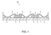
- FIG. 1 is a sectional view of an example of a light-emitting device manufactured according to a first embodiment.
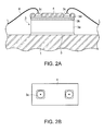
- FIGS. 2A and 2B are enlarged diagrams of a main part of the light-emitting device, wherein FIG. 2A is a sectional view and FIG. 2B is a plan view.
- a light-emitting device 10 shown in FIG. 1 and FIGS. 2A and 2B includes a substrate 1, wiring layers 2 formed on the substrate 1, LED chips 3 functioning as light-emitting elements, and phosphor layers 4.
- the substrate 1 is made of a flat plate of aluminum (Al), nickel (Ni), glass epoxy, ceramic, or the like having thermal radiation properties and rigidity.
- the substrate 1 desirably has thickness of 0.5 mm to 1.5 mm.
- heat conductivity at 25°C is equal to or higher than 30 W/m.K. If the thickness of the substrate 1 is smaller than 0.5 mm, strength of the substrate 1 is insufficient. It is likely that a crack occurs during attachment to an appliance or the like and during operation. If the thickness of the substrate 1 exceeds 1.5 mm, even if the heat conductivity is equal to or higher than 30 W/m.K, it is likely that the heat radiation properties of the entire substrate 1 are insufficient.
- the heat conductivity of the substrate 1 can be calculated from a temperature difference between a junction temperature and a substrate most cold point and the structure of the substrate 1 using, for example, a thermal resistance measuring device.
- the wiring layers 2 are layers mainly formed of conductive metal such as silver (Ag), gold (Au), or copper (Cu).
- the wiring layers 2 can be formed by printing (screen printing, inkjet printing, etc.) paste (ink) containing conductive powder (particulates) of Ag or the like on the surface of the substrate 1 in a desired pattern and then drying and baking an application layer.
- the LED chips 3 which are the light-emitting elements, for example, LED chips that emit blue light having main wavelength of 420 nm to 480 nm (e.g., 460 nm) or LED chips that emit an ultraviolet ray are used.
- the LED chips 3 are not limited to these LED chips.
- the LED chips 3 only have to be LED chips that radiate light and excite phosphors with the radiated light to generate visible light.
- Various light-emitting elements can be used according to the use of the light-emitting device 10, a target light emission color, and the like.
- the LED chip 3 has a structure in which a semiconductor light-emitting layer 3b is formed on an insulative element substrate 3a and a pair of electrodes 3c, 3c are formed on the semiconductor light-emitting layer 3b.
- the LED chip 3 is bonded (die-bonded) on the substrate 1 by an adhesive 5.
- the pair of electrodes 3c, 3c are respectively connected to the wiring layers 2 via bonding wires 6 such as metal wires.
- the LED chip 3 is mounted on the substrate 1 with its face up, i.e., with the surface on the formation side of the semiconductor light-emitting layer 3b faced up.
- the phosphor layer 4 is formed by electrostatically applying dispersed liquid, in which one or two or more kinds of phosphor particles are dispersed in liquid transparent resin, to the upper surface of the LED chip 3 mounted on the substrate 1 with its face up in this way and corners 3d continuous from the upper surface and thereafter hardening the applied resin.
- the phosphor layer 4 is formed at uniform or substantially uniform thickness on the upper surface of the LED chip 3 excluding forming portions of the element electrodes 3c, 3c and on the corners 3d continuous from the upper surface.
- the thickness means thickness at which "color unevenness” explained below does not occur when the light-emitting device is caused to emit light.
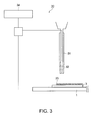
- FIG. 3 is a schematic diagram of an example of an electrostatic coating device 30 used for the formation of the phosphor layer 4.
- the electrostatic coating device 30 applies a pulse voltage between the substrate 1 mounted with the LED chip 3 and a spraying nozzle 31, draws out, with an electrostatic force of the pulse voltage, a liquid material (dispersed liquid in which phosphor particles are dispersed in liquid transparent resin) 32 at the distal end of the spraying nozzle 31 as very small liquid droplets 33, for example, liquid droplets of 50 ⁇ m to 100 ⁇ m, and attracts the very small liquid droplets 33 to the substrate 1 with an electric field to enable the liquid material 32 to be applied to the LED chip 3 on the substrate 1.
- a liquid material dispersed liquid in which phosphor particles are dispersed in liquid transparent resin
- the liquid material 32 can be applied to a required region from the upper surface to the side surfaces of the LED chip 3 by relatively moving the position of the distal end of the spraying nozzle 31 with respect to the substrate 1 in the horizontal direction or relatively changing the direction (the angle) of the distal end of the spraying nozzle 31.
- a uniform or substantially uniform film (the phosphor layer 4) can be formed by hardening the applied liquid material.
- the liquid material 32 is applied to the upper surface of the LED chip 3 excluding the forming portions of the element electrodes 3c, 3c and on the corners 3d continuous from the upper surface.
- the phosphor layer 4 having the uniform or substantially uniform thickness is formed in those regions.
- reference numeral 34 denotes a pulse voltage generating device.
- the LED chip 3 is not broken or the functions of the LED chip 3 are not lost by the pulse voltage applied between the substrate 1 and the spraying nozzle 31 by the pulse voltage generating device 34.
- liquid transparent resin used for the electrostatic application examples include silicone resin and epoxy resin. Above all, the use of the silicone resin is desirable from the viewpoint of light resistance, heat resistance, and the like.
- the phosphors various phosphors excited by the light from the LED chip 3 are used.
- a phosphor excited by blue light for example, a YAG phosphor such as an RE 3 (Al,Ga) 5 O 12 :Ce phosphor (RE indicates at least one kind selected from Y, Gd, and La) emitting a yellow light or an orange light, a silicate phosphor such as an AE 2 SiO 4 :Eu phosphor (AE is an alkali earth element such as Sr, Ba, or Ca.
- a YAG phosphor such as an RE 3 (Al,Ga) 5 O 12 :Ce phosphor (RE indicates at least one kind selected from Y, Gd, and La) emitting a yellow light or an orange light
- a silicate phosphor such as an AE 2 SiO 4 :Eu phosphor
- AE is an alkali earth element such as Sr, Ba, or Ca.
- a yellow phosphor such as a sialon phosphor (e.g., Ca x Si y Al z ON: Eu 2+ ), a YAG phosphor such as RE 3 (Al,Ga) 5 O 12 :Ce phosphor (RE indicates at least one kind selected from Y, Gd, and La.
- a silicate phosphor such as an AE 2 SiO 4 :Eu phosphor (AE is an alkali earth element such as Sr, Ba, or Ca.
- a sialon phosphor e.g., Ca x Si y Al z ON:Eu 2+
- a red phosphor such as a nitride phosphor (CASN) (e.g., CaAlSiN 3 :Eu) is used.
- SBN nitride phosphor
- an oxysulphide phosphor such as La 2 O 3 S:Eu 3+ phosphor, a germinate phosphor of manganese activated magnesium fluorogermanate (2.5MgO.MgF 2 :Mn 4+ ) or the like, a nitride phosphor (e.g., AE 2 Si 5 N 8 :Eu or CaAlSiN 3 :Eu), an oxynitride phosphor (e.g., Y 2 Si 3 O 3 N 4 :Ce), or a sialon phosphor (e.g., AE x (Si,Al) 12 (N,O) 16 :Eu) is used.
- a sialon phosphor e.g., AE x (Si,Al) 12 (N,O) 16 :Eu
- These phosphors are selected and used as appropriate according to a target light emission color or the like of the light-emitting device 10.
- phosphor particles having a particle diameter in micro order, i.e., a particle diameter of about several micrometers to several ten micrometers are used.
- the phosphor particles desirably have an average particle diameter of 3 ⁇ m to 20 ⁇ m and more desirably have an average diameter of 3 ⁇ m to 10 ⁇ m. If the average particle diameter of the phosphor particles is smaller than 3 ⁇ m, external quantum efficiency of the phosphors themselves falls and light emission efficiency falls. If the average particle diameter exceeds 20 ⁇ m, the particle diameter of liquid droplets increases. Depending on the size of the LED chip 3, it is likely that it may be difficult to selectively apply the liquid material 32 to the required region at the uniform thickness explained above.
- the particle diameter and the average particle diameter of the phosphors can be calculated by, for example, a laser diffraction particle size analyzer.
- the average particle diameter is a particle diameter at which loading weight is 50% in a particle size distribution measured by the analyzer.
- the phosphor layer 4 is formed as a homogenous layer as a whole using one kind of dispersed liquid in which one or two or more kinds phosphor particles are uniformly dispersed in the liquid transparent resin.
- different phosphors or the like may be contained depending on regions using two or more kinds of dispersed liquid having different compositions.
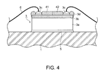
- the upper surface of the LED chip 3 is divided into two regions. Phosphor layers 41 and 42 containing different phosphors are respectively formed in the regions.
- the phosphor layers 41 and 42 containing different phosphors are provided to be vertically laminated.
- an inorganic filler having satisfactory heat conductivity and optical transparency can be contained in the dispersed liquid together with the phosphor particles.
- the inorganic filler only has to be an inorganic filler having satisfactory heat conductivity and optical transparency.
- powder of silica, tantalum oxide (TaO), or zinc oxide (ZnO) is used.
- These inorganic fillers can be used independently or two or more kinds of the inorganic fillers can be mixed and used.
- An inorganic filler having a particle diameter smaller than the particle diameter of the phosphors in use is desirably used.
- the particle diameter of the inorganic filler can be calculated by, for example, a laser diffraction particle size analyzer.
- An inorganic filler having a particle diameter in submicron order, i.e., a particle diameter of about several hundred nanometers is desirably used.
- the phosphor layer 4 is formed by the electrostatic application, the phosphor layer 4 is formed in substantially uniform thickness on the upper surface of the LED chip 3 excluding the forming portions of the element electrodes 3c, 3c and on the corners 3d continuous from the upper surface. Therefore, the heat conduction from the phosphor to the LED chip 3 can be improved and the heat radiation properties can be improved. Therefore, it is possible to sufficiently cope with the increase in power of a light-emitting device in recent years and realize light emission at a large light amount and high efficiency. Since phosphors do not excessively adhere, it is possible to reduce a phosphor amount.
- the thickness is uniform, it is possible to suppress occurrence of color unevenness. If the thickness is non-uniform and the phosphor layer 4 is not provided on the corners 3d of the LED chip 3 or the thickness of the phosphor layer 4 is insufficient, it is likely that light radiated from the LED chip 3 leaks to the outside from the corners 3d and, for example, in the case of the LED chip that emits blue light, a so-called blue ring phenomenon occurs. In the light-emitting device 10 according to this embodiment, since the required phosphor layer having thickness substantially equal to the thickness of the upper layer is also provided on the corners 3d, such a blue ring phenomenon does not occur.
- This embodiment has an advantage that, in particular, even if the LED chip 3 is, for example, an LED chip of a very small size of 0.2mmx0.2mm having an area of 0.04 mm 2 , it is possible to selectively form the phosphor layer 4 at uniform thickness and in a required region.
- the LED chip 3 is, for example, an LED chip of a very small size of 0.2mmx0.2mm having an area of 0.04 mm 2 , it is possible to selectively form the phosphor layer 4 at uniform thickness and in a required region.
- a jet dispenser method since the size of liquid droplets is large (a minimum size of about 200 ⁇ m), it may be substantially impossible to selectively form a phosphor layer at equal thickness and in a required region.
- a spray coat method it is possible to apply a liquid material to a selective region by using a mask.
- this method is originally a method of applying the liquid material to a large area. Therefore, this method is not suitable as a method of applying the liquid material to each chip. It may
- the liquid material can be applied as the liquid droplets of 50 ⁇ m to 100 ⁇ m, even if the LED chip is the LED chip of the very small size, it is possible to selectively apply the liquid material to a required region and at uniform or substantially uniform thickness.
- the phosphor layer 4 is formed only on the upper surface and the corners 3d of the LED chip 3. This is because, in this embodiment, the LED chip 3 is mounted on the substrate 1 with its face up and, in this case, the semiconductor light-emitting layer 3b of the LED chip 3 is present on the upper surface side and the light from the LED chip 3 is emitted only from the upper surface of the LED chip 3 and the corners 3d continuous from the upper surface. In this embodiment, since the electrostatic application is used for the formation of the phosphor layer 4, it is possible to easily perform such selective application.
- the light-emitting device in which the phosphor layer is provided over the entire surface of the LED chip 3 it is possible to reduce an amount of use of phosphors. Further, it is possible to obtain the light-emitting device 10 having a satisfactory light emission characteristic.
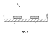
- FIG. 6 is a sectional view of an example of a light-emitting device manufactured according to a second embodiment.
- FIG. 7 is an enlarged sectional view of a main part of the light-emitting device.
- this embodiment to avoid redundant explanation, explanation of similarities to the first embodiment is omitted or simplified and differences from the first embodiment are mainly explained.
- a light-emitting device 20 shown in FIGS. 6 and 7 includes the substrate 1, a wiring layer (not shown in the figures) formed on the substrate 1, the LED chips 3 functioning as light-emitting elements, and the phosphor layers 4.
- the LED chip 3 is mounted on the substrate 1 with its face down, i.e., mounted by flip-chip mounting for directly connecting the element electrode 3c of the LED chip 3 to an electrode 2a of the wiring layer on the substrate 1.
- the semiconductor light-emitting layer 3b formed on the LED chip 3 is located on the substrate 1 side. Light emitted from the semiconductor light-emitting layer 3b is emitted from not only the upper surface of the LED chip 3 (a surface on the opposite side of a surface on which the element electrodes 3c are formed) but also the side surfaces of the LED chip 3.
- the phosphor layer 4 is provided to cover the entire surface of the LED chip 3, i.e., provided on all of the upper surface, the side surfaces, and the corners 3d of the LED chip 3.
- the phosphor layer 4 is formed by electrostatically applying dispersed liquid by, for example, the electrostatic coating device 30 shown in FIG. 3 and hardening the dispersed liquid.
- the phosphor layer 4 is formed at substantially uniform thickness.
- the phosphor layer 4 may be formed to contain different phosphors or the like depending on regions using two or more kinds of dispersed liquid having different compositions.
- an inorganic filler having satisfactory heat conductivity and optical transparency for example, powder of silica, tantalum oxide (TaO), or zinc oxide (ZnO) can be contained in the dispersed liquid together with the phosphor particles.
- An inorganic filler having a particle diameter smaller than the particle diameter of the phosphors in use is desirably used.
- the phosphor layer 4 since the phosphor layer 4 is formed by the electrostatic application, the phosphor layer 4 can be formed in substantially uniform thickness. Therefore, the heat conduction from the phosphor to the LED chip 3 can be improved and the heat radiation properties can be improved. Therefore, it is possible to sufficiently cope with the increase in power of a light-emitting device in recent years and realize light emission at a large light amount and high efficiency. Since phosphors do not excessively adhere, it is possible to reduce a phosphor amount.
- the thickness is uniform, it is possible to suppress occurrence of color unevenness. Further, it is possible to prevent occurrence of the blue ring phenomenon that occurs when if the phosphor layer 4 is not sufficiently provided on the corners 3d of the LED chip 3.
- the LED chip 3 is, for example, an LED chip of a very small size of 0.2mmx0.2mm having an area of 0.04 mm 2 , it is possible to form the phosphor layer 4 at uniform thickness.
- the phosphor layer is formed by electrostatically applying the dispersed liquid in which the phosphor particles are dispersed in the liquid transparent resin.
- electrostatic spraying can also be used instead of the electrostatic application.
- liquid droplets are refined by charging and sprayed.
- the electrostatic spraying since the liquid droplets are sprayed to spread from above to under an object (an LED chip), it may be difficult to form a uniform film to side surfaces of the LED chip. Therefore, as in the second embodiment, if it is necessary to form a phosphor layer to the side surfaces of the LED chip, it is desirable to use the electrostatic application. As in the first embodiment, if the phosphor layer is formed on the upper surface of the LED chip and the corners continuous from the upper surface, either the electrostatic application or the electrostatic spraying may be used.
- Plural blue LED chips (575 ⁇ m ⁇ 325 ⁇ m ⁇ 170 ⁇ m, electrode pads of ⁇ 70 ⁇ m) that emitted blue light having wavelength of 450 nm to 460 nm were bonded on a ceramics substrate, which was provided with an Ag wiring layer, by a silicone adhesive.
- the blue LED chip and the Ag wiring layer on the ceramic substrate were electrically joined by wire bonding.
- Dispersed liquid of the phosphors was electrostatically applied to the upper surface of the LED chip on the ceramics substrate and corners continuous from the upper surface (excluding the electrode pads) to be hardened using the electrostatic coating device (spraying nozzle distal end diameter: 1. 6 mm) 30 shown in FIG. 3 . Then, the light-emitting device 10 including a phosphor layer having substantially uniform thickness on the upper surface of the LED chip and the corners continuous from the upper surface (excluding the electrode pads) was manufactured.
- a comparative example 1 manufacturing of a light-emitting device having the same configuration as the example 1 was attempted in the same manner as the example 1 except that a jet dispenser (liquid droplet diameter: about 200 ⁇ m) was used instead of the electrostatic coating device 30.
- a jet dispenser liquid droplet diameter: about 200 ⁇ m
- a phosphor layer having uniform thickness was unable to be formed on the upper surface of the LED chip and the corners continuous from the upper surface (excluding the electrode pads).
- a light-emitting device was manufactured in the same manner as the example 1 except that a blue LED chip (200 ⁇ m ⁇ 200 ⁇ m ⁇ 170 ⁇ m, electrode pads of ⁇ 70 ⁇ m) was used as the LED chip 3, a phosphor layer having uniform thickness was able to be formed on the upper surface of the LED chip on the ceramics substrate and the corners continuous from the upper surface (excluding the electrode pads).
- a blue LED chip 200 ⁇ m ⁇ 200 ⁇ m ⁇ 170 ⁇ m, electrode pads of ⁇ 70 ⁇ m
- a blue LED chip (800 ⁇ m ⁇ 800 ⁇ m ⁇ 170 ⁇ m, electrode pads of ⁇ 150 ⁇ m) was used as the LED chip 3, the LED chip was AuSn-flip-chip joined on the ceramics substrate 1, phosphor containing dispersed liquid prepared in the same manner as in the example 1 was applied to the upper surface, the side surfaces, and the corners of the LED chip of the ceramics substrate to be hardened using the electrostatic coating device (spraying nozzle distal end diameter: 1.6 mm) 30 shown in FIG. 3 . Then, a light-emitting device having a phosphor layer having substantially uniform thickness on the upper surface, the side surfaces, and the corners of the LED chip was manufactured. When the obtained light-emitting device was caused to emit light, light without color unevenness was obtained and the blue ring phenomenon was not observed.
Landscapes
- Led Device Packages (AREA)
- Encapsulation Of And Coatings For Semiconductor Or Solid State Devices (AREA)
Applications Claiming Priority (1)
| Application Number | Priority Date | Filing Date | Title |
|---|---|---|---|
| JP2011208949A JP6066253B2 (ja) | 2011-09-26 | 2011-09-26 | 発光装置の製造方法 |
Publications (2)
| Publication Number | Publication Date |
|---|---|
| EP2573828A2 true EP2573828A2 (fr) | 2013-03-27 |
| EP2573828A3 EP2573828A3 (fr) | 2014-12-31 |
Family
ID=46796307
Family Applications (1)
| Application Number | Title | Priority Date | Filing Date |
|---|---|---|---|
| EP12180282.1A Withdrawn EP2573828A3 (fr) | 2011-09-26 | 2012-08-13 | Procédé de fabrication d'un dispositif électroluminescent et dispositif électroluminescent |
Country Status (4)
| Country | Link |
|---|---|
| US (1) | US20130076230A1 (fr) |
| EP (1) | EP2573828A3 (fr) |
| JP (1) | JP6066253B2 (fr) |
| CN (1) | CN103022322A (fr) |
Cited By (2)
| Publication number | Priority date | Publication date | Assignee | Title |
|---|---|---|---|---|
| JP2014192502A (ja) * | 2013-03-28 | 2014-10-06 | Toyoda Gosei Co Ltd | 発光装置の製造方法 |
| WO2016172753A1 (fr) * | 2015-04-29 | 2016-11-03 | Tridonic Jennersdorf Gmbh | Procédé de fabrication d'un module à del |
Families Citing this family (9)
| Publication number | Priority date | Publication date | Assignee | Title |
|---|---|---|---|---|
| DE102012208900A1 (de) | 2012-05-25 | 2013-11-28 | Osram Opto Semiconductors Gmbh | Verfahren zum Herstellen optoelektronischer Bauelemente und Vorrichtung zum Herstellen optoelektronischer Bauelemente |
| DE102013103416A1 (de) * | 2013-04-05 | 2014-10-23 | Osram Opto Semiconductors Gmbh | Elektromagnetische Strahlung emittierende Baugruppe und Verfahren zum Herstellen einer elektromagnetische Strahlung emittierenden Baugruppe |
| JP6307703B2 (ja) * | 2013-05-31 | 2018-04-11 | パナソニックIpマネジメント株式会社 | 波長変換素子、波長変換素子を備えた発光装置、発光装置を備えた車両、および波長変換素子の製造方法 |
| JP6011487B2 (ja) * | 2013-08-09 | 2016-10-19 | 豊田合成株式会社 | Ledランプの製造方法及び封止材の枡型装置 |
| JP6229412B2 (ja) * | 2013-09-30 | 2017-11-15 | 日亜化学工業株式会社 | 発光装置の製造方法 |
| CN104576889B (zh) * | 2013-10-17 | 2018-10-26 | 刘艳 | 在led芯片上形成荧光层的方法 |
| EP3092667B1 (fr) | 2014-01-06 | 2019-04-24 | Lumileds Holding B.V. | Flash mince à del pour caméra |
| CN106711313B (zh) * | 2016-12-29 | 2019-05-14 | 浙江瑞丰光电有限公司 | 一种荧光片的封装方法及一种led封装器件 |
| DE102021105601A1 (de) | 2020-07-03 | 2022-01-05 | Hoya Corporation | Beleuchtungsvorrichtung |
Citations (1)
| Publication number | Priority date | Publication date | Assignee | Title |
|---|---|---|---|---|
| JPH10319877A (ja) | 1997-05-16 | 1998-12-04 | Toshiba Corp | 画像表示装置及び発光装置 |
Family Cites Families (31)
| Publication number | Priority date | Publication date | Assignee | Title |
|---|---|---|---|---|
| US7470547B2 (en) * | 2003-07-31 | 2008-12-30 | Biodot, Inc. | Methods and systems for dispensing sub-microfluidic drops |
| JP3589187B2 (ja) * | 2000-07-31 | 2004-11-17 | 日亜化学工業株式会社 | 発光装置の形成方法 |
| JP2002184306A (ja) * | 2000-12-12 | 2002-06-28 | Harison Toshiba Lighting Corp | 蛍光ランプの製造方法 |
| JP2002373781A (ja) * | 2001-03-29 | 2002-12-26 | Hitachi Ltd | 有機el表示体、及びカラーフィルターの製造装置 |
| TWI264963B (en) * | 2001-03-29 | 2006-10-21 | Hitachi Ltd | Organic EL display and production device of color filter |
| US6576488B2 (en) * | 2001-06-11 | 2003-06-10 | Lumileds Lighting U.S., Llc | Using electrophoresis to produce a conformally coated phosphor-converted light emitting semiconductor |
| CN1323441C (zh) * | 2001-10-12 | 2007-06-27 | 日亚化学工业株式会社 | 发光装置及其制造方法 |
| JP2004119634A (ja) * | 2002-09-25 | 2004-04-15 | Toshiba Lighting & Technology Corp | 発光装置 |
| JP4082181B2 (ja) * | 2002-11-08 | 2008-04-30 | 松下電器産業株式会社 | パターン形成方法 |
| JP4415572B2 (ja) * | 2003-06-05 | 2010-02-17 | 日亜化学工業株式会社 | 半導体発光素子およびその製造方法 |
| JP4325343B2 (ja) * | 2003-09-25 | 2009-09-02 | セイコーエプソン株式会社 | 膜形成方法およびデバイス製造方法 |
| JP2005223165A (ja) * | 2004-02-06 | 2005-08-18 | Sanyo Electric Co Ltd | 窒化物系発光素子 |
| DE102004060358A1 (de) * | 2004-09-30 | 2006-04-13 | Osram Opto Semiconductors Gmbh | Verfahren zum Herstellen von Lumineszenzdiodenchips und Lumineszenzdiodenchip |
| ATE537564T1 (de) * | 2004-10-13 | 2011-12-15 | Panasonic Corp | Lumineszente lichtquelle, verfahren zu ihrer herstellung und licht emittierende vorrichtung |
| KR100674831B1 (ko) * | 2004-11-05 | 2007-01-25 | 삼성전기주식회사 | 백색 발광 다이오드 패키지 및 그 제조방법 |
| JP2006154032A (ja) * | 2004-11-26 | 2006-06-15 | Nichia Chem Ind Ltd | 画像表示装置 |
| TWI389337B (zh) * | 2005-05-12 | 2013-03-11 | 松下電器產業股份有限公司 | 發光裝置與使用其之顯示裝置及照明裝置,以及發光裝置之製造方法 |
| JP4745062B2 (ja) * | 2005-06-02 | 2011-08-10 | 三星モバイルディスプレイ株式會社 | 平板表示装置及びその製造方法 |
| JP4742697B2 (ja) * | 2005-06-27 | 2011-08-10 | パナソニック電工株式会社 | 塗装装置 |
| JP2009512178A (ja) * | 2005-11-04 | 2009-03-19 | パナソニック株式会社 | 発光モジュールとこれを用いた表示装置及び照明装置 |
| JP4311429B2 (ja) * | 2006-09-27 | 2009-08-12 | セイコーエプソン株式会社 | 有機エレクトロルミネッセンス装置の製造方法、及び有機エレクトロルミネッセンス装置 |
| JP4859050B2 (ja) * | 2006-11-28 | 2012-01-18 | Dowaエレクトロニクス株式会社 | 発光装置及びその製造方法 |
| US20080121911A1 (en) * | 2006-11-28 | 2008-05-29 | Cree, Inc. | Optical preforms for solid state light emitting dice, and methods and systems for fabricating and assembling same |
| US8668843B2 (en) * | 2007-03-28 | 2014-03-11 | Hiroshima University | M-C-N-O based phosphor |
| CN101465328A (zh) * | 2007-12-21 | 2009-06-24 | 深圳富泰宏精密工业有限公司 | 发光二极管封装及其制造方法 |
| US8940561B2 (en) * | 2008-01-15 | 2015-01-27 | Cree, Inc. | Systems and methods for application of optical materials to optical elements |
| US8714776B2 (en) * | 2008-05-13 | 2014-05-06 | Research Triangle Institute | Porous and non-porous nanostructures and application thereof |
| JP2010064359A (ja) * | 2008-09-11 | 2010-03-25 | Engineering System Kk | 静電式液滴吐出機構およびマルチノズルユニット |
| TWI398020B (zh) * | 2008-12-01 | 2013-06-01 | Ind Tech Res Inst | 發光裝置 |
| US7897419B2 (en) * | 2008-12-23 | 2011-03-01 | Cree, Inc. | Color correction for wafer level white LEDs |
| US9275979B2 (en) * | 2010-03-03 | 2016-03-01 | Cree, Inc. | Enhanced color rendering index emitter through phosphor separation |
-
2011
- 2011-09-26 JP JP2011208949A patent/JP6066253B2/ja not_active Expired - Fee Related
-
2012
- 2012-08-13 EP EP12180282.1A patent/EP2573828A3/fr not_active Withdrawn
- 2012-08-29 US US13/598,233 patent/US20130076230A1/en not_active Abandoned
- 2012-08-30 CN CN2012103144759A patent/CN103022322A/zh active Pending
Patent Citations (1)
| Publication number | Priority date | Publication date | Assignee | Title |
|---|---|---|---|---|
| JPH10319877A (ja) | 1997-05-16 | 1998-12-04 | Toshiba Corp | 画像表示装置及び発光装置 |
Cited By (3)
| Publication number | Priority date | Publication date | Assignee | Title |
|---|---|---|---|---|
| JP2014192502A (ja) * | 2013-03-28 | 2014-10-06 | Toyoda Gosei Co Ltd | 発光装置の製造方法 |
| WO2016172753A1 (fr) * | 2015-04-29 | 2016-11-03 | Tridonic Jennersdorf Gmbh | Procédé de fabrication d'un module à del |
| AT16795U1 (de) * | 2015-04-29 | 2020-09-15 | Tridonic Jennersdorf Gmbh | Verfahren zum Herstellen eines LED-Moduls |
Also Published As
| Publication number | Publication date |
|---|---|
| JP2013069980A (ja) | 2013-04-18 |
| CN103022322A (zh) | 2013-04-03 |
| US20130076230A1 (en) | 2013-03-28 |
| JP6066253B2 (ja) | 2017-01-25 |
| EP2573828A3 (fr) | 2014-12-31 |
Similar Documents
| Publication | Publication Date | Title |
|---|---|---|
| US20130076230A1 (en) | Manufacturing method of light-emitting device and the light-emitting device | |
| JP7414886B2 (ja) | 発光素子及びその製造方法 | |
| JP5680278B2 (ja) | 発光装置 | |
| JP6149487B2 (ja) | 発光装置の製造方法および発光装置 | |
| US7839087B2 (en) | Light emitting device and method of manufacturing the same | |
| JP6079209B2 (ja) | 発光装置およびその製造方法 | |
| KR101847938B1 (ko) | 발광소자 패키지 및 그 제조 방법 | |
| CN106134297B (zh) | 发光装置用基板、发光装置及照明装置 | |
| CN107275301B (zh) | 发光装置 | |
| JP6387954B2 (ja) | 波長変換部材を用いた発光装置の製造方法 | |
| JP4473284B2 (ja) | 発光装置およびその製造方法 | |
| JP6290380B2 (ja) | 発光装置用基板、発光装置、及び、発光装置用基板の製造方法 | |
| JPWO2005091387A1 (ja) | 発光装置および照明装置 | |
| JP2008060542A (ja) | 発光装置、発光装置の製造方法、及びこれを備えた光源装置 | |
| JP6959502B2 (ja) | 発光装置 | |
| TW201724573A (zh) | 發光裝置以及其製造方法 | |
| JP6097040B2 (ja) | 半導体発光装置およびその製造方法 | |
| JP7389333B2 (ja) | 発光装置 | |
| JP5082427B2 (ja) | 発光装置 | |
| JP6426332B2 (ja) | 発光装置 | |
| JP6985615B2 (ja) | 発光装置 | |
| JP2024020049A (ja) | 配線基板、発光装置及びそれらの製造方法 | |
| JP2007116116A (ja) | 発光装置 | |
| KR20120104762A (ko) | 발광 소자 모듈 및 그 제조 방법 | |
| US20260095021A1 (en) | Method of manufacturing light-emitting device |
Legal Events
| Date | Code | Title | Description |
|---|---|---|---|
| PUAI | Public reference made under article 153(3) epc to a published international application that has entered the european phase |
Free format text: ORIGINAL CODE: 0009012 |
|
| 17P | Request for examination filed |
Effective date: 20120813 |
|
| AK | Designated contracting states |
Kind code of ref document: A2 Designated state(s): AL AT BE BG CH CY CZ DE DK EE ES FI FR GB GR HR HU IE IS IT LI LT LU LV MC MK MT NL NO PL PT RO RS SE SI SK SM TR |
|
| AX | Request for extension of the european patent |
Extension state: BA ME |
|
| PUAL | Search report despatched |
Free format text: ORIGINAL CODE: 0009013 |
|
| AK | Designated contracting states |
Kind code of ref document: A3 Designated state(s): AL AT BE BG CH CY CZ DE DK EE ES FI FR GB GR HR HU IE IS IT LI LT LU LV MC MK MT NL NO PL PT RO RS SE SI SK SM TR |
|
| AX | Request for extension of the european patent |
Extension state: BA ME |
|
| RIC1 | Information provided on ipc code assigned before grant |
Ipc: H01L 33/50 20100101AFI20141126BHEP Ipc: H01L 33/64 20100101ALN20141126BHEP |
|
| STAA | Information on the status of an ep patent application or granted ep patent |
Free format text: STATUS: THE APPLICATION HAS BEEN WITHDRAWN |
|
| 18W | Application withdrawn |
Effective date: 20150112 |