EP2574937A2 - Schneller Wechselspannungsdetektor - Google Patents
Schneller Wechselspannungsdetektor Download PDFInfo
- Publication number
- EP2574937A2 EP2574937A2 EP12184374A EP12184374A EP2574937A2 EP 2574937 A2 EP2574937 A2 EP 2574937A2 EP 12184374 A EP12184374 A EP 12184374A EP 12184374 A EP12184374 A EP 12184374A EP 2574937 A2 EP2574937 A2 EP 2574937A2
- Authority
- EP
- European Patent Office
- Prior art keywords
- voltage
- output
- threshold
- transistor
- waveform
- Prior art date
- Legal status (The legal status is an assumption and is not a legal conclusion. Google has not performed a legal analysis and makes no representation as to the accuracy of the status listed.)
- Granted
Links
Images


Classifications
-
- G—PHYSICS
- G01—MEASURING; TESTING
- G01R—MEASURING ELECTRIC VARIABLES; MEASURING MAGNETIC VARIABLES
- G01R19/00—Arrangements for measuring currents or voltages or for indicating presence or sign thereof
- G01R19/145—Indicating the presence of current or voltage
- G01R19/155—Indicating the presence of voltage
-
- G—PHYSICS
- G01—MEASURING; TESTING
- G01R—MEASURING ELECTRIC VARIABLES; MEASURING MAGNETIC VARIABLES
- G01R19/00—Arrangements for measuring currents or voltages or for indicating presence or sign thereof
- G01R19/165—Indicating that current or voltage is either above or below a predetermined value or within or outside a predetermined range of values
- G01R19/16533—Indicating that current or voltage is either above or below a predetermined value or within or outside a predetermined range of values characterised by the application
- G01R19/16538—Indicating that current or voltage is either above or below a predetermined value or within or outside a predetermined range of values characterised by the application in AC or DC supplies
- G01R19/16547—Indicating that current or voltage is either above or below a predetermined value or within or outside a predetermined range of values characterised by the application in AC or DC supplies voltage or current in AC supplies
Definitions
- the present disclosure relates to power control circuit testing, and more specifically to AC voltage detection for load power application and removal timing.
- Power control circuit testing involves timing when a load is applied to, or removed from, a circuit.
- One method used to perform this monitoring is to monitor the voltage at a load output.
- a peak detector is used. Peak detectors rectify and filter the AC output and sense the resulting voltage levels to determine if a load is being driven by an AC power source.
- An AC voltage being applied to the load is detected when the output voltage of the peak detector crosses from below an upper detection threshold to above the upper detection threshold.
- a capacitor in the detection circuit then holds the voltage between peaks for 1 ⁇ 2 cycle of the input AC waveform above the upper detection threshold in order to prevent false load state changed events.
- a load detection circuit using a capacitor in this manner is to be referred to as a capacitive hold AC voltage detector.
- the capacitor When a load is removed from the circuit, the capacitor slowly discharges and the removal of the load is detected when the voltage falls below a lower detector threshold.
- the slow discharge is due to the presence of the capacitor and relatively the large capacitance values that must be used to prevent false output changes when AC power is applied or removed from the monitored load.
- a fast AC voltage detector has a bridge rectifier with inputs for connecting to an AC power source, a threshold detector connected to the output of the bridge rectifier, an isolation circuit connected to the output of the threshold detector, a continuous voltage averager connected to an output of the isolation circuit, and a Schmidt trigger amplifier connected to the continuous voltage averager and operable to output a first voltage level when AC voltage is present on the bridge rectifier inputs and a second voltage level when no AC voltage is present on the bridge rectifier inputs.
- a method for detecting a load includes the steps of converting an AC waveform to a continuous average square wave representation of the AC waveform, detecting a presence of a load when the continuous average square wave crosses a load applied threshold, and detecting the removal of the load when the continuous average square wave crosses a load removed threshold.
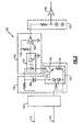
- FIG. 1 illustrates a fast AC voltage detector 10 for detecting the application of, or the removal of, an AC power source 20 from a load.
- the fast AC voltage detector 10 has a bridge rectifier 40 that rectifies the AC signal from the power source 20 into a full wave rectified AC signal.
- the full wave rectified AC signal is passed to a Zener driven constant current source 50 that forces the full wave rectified AC signal into a square wave representative of the full wave rectified AC signal.
- the square wave has a peak when the voltage of the full wave rectified AC signal exceeds the conduction threshold of a Zener diode 54, and a valley when the full wave rectified AC signal does not exceed the Zener diode 54 conduction threshold.
- the square wave signal is passed through an isolation amplifier 60 and to a resistive/capacitive (RC) voltage averager 70.
- the RC voltage averager 70 outputs a continuing average of the square wave signal. Alternately, any other continuing voltage average can be used in place of the RC voltage average 70.
- the continuing average signal is passed from the RC voltage average 70 to a Schmidt trigger 80.
- the Schmidt trigger 80 detects an application of a load by detecting when the continuing average signal crosses from below an upper detection threshold to above the upper detection threshold. Likewise, the Schmidt trigger detects a load being removed by detecting the continuing average signal crossing from above a lower detection threshold to below the lower detection threshold.
- the Schmidt trigger outputs a high signal while there is no load applied and a low signal (0V) when a load is present, thereby providing a load detection signal for any attached controllers.
- FIG. 2 illustrates the example AC voltage detector 10 of Figure 1 in greater detail.
- Figures 3A, 3B, and 3C illustrate the AC power source 20 output signal as it progresses through the AC voltage detector 100 of Figure 2 .
- the bridge rectifier 140 is a standard AC full wave rectifier that accepts inputs 142, 144 from a load or power source, and outputs a full wave rectified AC waveform (illustrated in Figure 3A ) to a Zener diode and Zener driven constant current source segment 150 of the AC voltage detector 100.
- the Zener driven constant current source 152 is connected to the opto-isolator 160 via a transistor 156 within the Zener driven constant current source 152.
- the transistor 156 receives a control input from the anode of the Zener diode 154.
- the transistor 156 control input 157 receives a signal and the transistor 156 enters a closed state, thereby allowing current to pass.
- the transistor 156, a pair of diodes 158 and a resistor 159 operate as a constant current source and output a steady current to the opto-isolator 160.
- the Zener driven constant current source 152 converts the AC waveform of Figure 3A to a square wave output illustrated in Figure 3B .
- the exact threshold voltage of the Zener diode 154 depends on the minimum to maximum range of the input voltage to be detected.
- the threshold voltage is high enough to avoid false input detection from leaky power control devices such as those employing resistor-capacitor snubber circuits, but low enough that the minimum input voltage to be detected will produce a square wave with a longer on time than off time at the threshold detector's output.
- the isolation amplifier 160 isolates square wave output of the Zener driven constant current source 152 from an RC voltage averager 170, thereby preventing the propagation of potentially harmful voltage and transient signals from the power sources at 142 and 144 to the timing circuits of an attached controller.
- the particular isolator 161 used for the isolation amplifier 160 in the illustrated example is a standard light emitting diode optically coupled to a photosensitive transistor in a single component package referred to as an optical isolator or opto-isolator.
- the square wave signal from the optical isolator 161 is sent to a standard Schmidt trigger 162 to preserve the rise and fall times of the waveform and provide sufficient drive capability for following circuits.
- the signal is passed to a RC voltage averager 170 that performs a continuing averaging function on the square wave.
- the RC voltage averager 170 causes the valleys of the square wave function to be averaged up, resulting in a continuing average signal illustrated in Figure 3C , and corresponding to the square wave signal of Figure 3B and the full wave rectified signal of Figure 3A .
- the time constant of the RC voltage averager 170 is adjusted for minimum reliable detection delay for the lowest AC frequency to be detected.
- the continuing average signal illustrated in Figure 3C is passed to a standard Schmidt trigger circuit 180 that detects the application of the load whenever the voltage of the continuing average voltage signal exceeds a load applied threshold 220. Likewise the Schmidt trigger detects that a load has been removed from the circuit whenever the continuing average signal drops below a load removed threshold 230.
- the continuing average wave drops off significantly faster than systems using a capacitive hold AC power detector.
- the waveform in figure 3B being a square wave, has much less time between peaks than the waveform in figure 3A . Therefore the waveform averaging circuit 70 has a much faster response than the peak holding circuit that must filter a waveform similar to the waveform illustrated in figure 3A .
- the continuous averaging detection provided by the above described system detects the application and/or removal of a load faster than a capacitive hold system.
- the above described system can detect the removal of a load in less than 1 ⁇ 4 of a cycle of the AC waveform, whereas a capacitive hold system can take many cycles before it detects the removal of the load.
Landscapes
- Physics & Mathematics (AREA)
- General Physics & Mathematics (AREA)
- Rectifiers (AREA)
- Measurement Of Current Or Voltage (AREA)
Applications Claiming Priority (1)
| Application Number | Priority Date | Filing Date | Title |
|---|---|---|---|
| US13/248,583 US8933688B2 (en) | 2011-09-29 | 2011-09-29 | Fast AC voltage detector |
Publications (3)
| Publication Number | Publication Date |
|---|---|
| EP2574937A2 true EP2574937A2 (de) | 2013-04-03 |
| EP2574937A3 EP2574937A3 (de) | 2016-10-19 |
| EP2574937B1 EP2574937B1 (de) | 2018-07-18 |
Family
ID=47071110
Family Applications (1)
| Application Number | Title | Priority Date | Filing Date |
|---|---|---|---|
| EP12184374.2A Active EP2574937B1 (de) | 2011-09-29 | 2012-09-14 | Schneller Wechselspannungsdetektor |
Country Status (2)
| Country | Link |
|---|---|
| US (1) | US8933688B2 (de) |
| EP (1) | EP2574937B1 (de) |
Cited By (3)
| Publication number | Priority date | Publication date | Assignee | Title |
|---|---|---|---|---|
| GB2537692A (en) * | 2015-04-23 | 2016-10-26 | Tridonic Gmbh & Co Kg | Detection circuit for detecting a supply voltage |
| CN106383263A (zh) * | 2016-10-28 | 2017-02-08 | 阳光电源股份有限公司 | 一种离网逆变器负载检测方法及控制器 |
| CN113406382A (zh) * | 2021-07-12 | 2021-09-17 | 华中科技大学 | 一种低成本配电网pmu及其工作方法 |
Families Citing this family (5)
| Publication number | Priority date | Publication date | Assignee | Title |
|---|---|---|---|---|
| US8901915B2 (en) * | 2012-01-11 | 2014-12-02 | Elster Solutions, Llc | Voltage or contact closure sensor |
| JP7056058B2 (ja) * | 2017-09-29 | 2022-04-19 | ブラザー工業株式会社 | 交流電圧検出装置、画像形成装置および産業機械 |
| US11860211B2 (en) * | 2021-12-08 | 2024-01-02 | Ford Global Technologies, Llc | System for monitoring a high voltage electrical system in a vehicle |
| CN117289116A (zh) * | 2023-11-27 | 2023-12-26 | 成都锐成芯微科技股份有限公司 | 一种施密特触发器的测试方法 |
| CN118068076B (zh) * | 2024-02-28 | 2024-09-24 | 中国铁道科学研究院集团有限公司 | 一种交流电压测量电路 |
Family Cites Families (21)
| Publication number | Priority date | Publication date | Assignee | Title |
|---|---|---|---|---|
| US4782422A (en) | 1987-07-27 | 1988-11-01 | Sundstrand Corporation | I2 t monitoring circuit |
| US5047914A (en) | 1989-11-21 | 1991-09-10 | Sundstrand Corporation | Current controlled inverter |
| FR2706699B1 (fr) * | 1993-06-10 | 1995-09-15 | Gec Alsthom T & D Sa | Dispositif pour la fourniture d'une tension à un circuit électronique, en particulier à un circuit électronique associé à un capteur d'intensité placé sur une ligne électrique. |
| US5675640A (en) * | 1995-05-19 | 1997-10-07 | Lucent Technologies Inc. | Telephone ringing signal detector |
| KR0175447B1 (ko) * | 1995-12-26 | 1999-04-01 | 김광호 | 유무선 복합전화기의 링 검출회로 및 방법 |
| US6104622A (en) * | 1997-04-30 | 2000-08-15 | Fidelix Y.K. | Power supply apparatus for reduction of power consumption |
| US5949158A (en) * | 1997-05-05 | 1999-09-07 | Gerhard Kurz | Method and arrangement for controlling the output of electrical consumers connected to an AC line voltage |
| JP3437410B2 (ja) * | 1997-06-02 | 2003-08-18 | シャープ株式会社 | ヒータ制御装置 |
| US6538478B2 (en) | 2000-11-28 | 2003-03-25 | Texas Instruments Incorporated | Noise immune peak detector |
| US6774617B2 (en) | 2000-11-28 | 2004-08-10 | Texas Instruments Incorporated | Peak detector for detecting a peak signal |
| US6535033B2 (en) | 2000-12-07 | 2003-03-18 | Texas Instruments Incorporated | Peak hold circuit |
| US7548441B2 (en) * | 2004-02-24 | 2009-06-16 | Vlt, Inc. | Universal AC adapter |
| US7741828B2 (en) * | 2004-05-18 | 2010-06-22 | Thomson Licensing | Power disturbance detection circuit and method |
| US20070047270A1 (en) * | 2005-09-01 | 2007-03-01 | Creative Technology Ltd. | Load detector for an AC-AC power supply |
| US7205756B1 (en) | 2005-10-19 | 2007-04-17 | Hamilton Sundstrand Corporation | Unbalanced current detection |
| US7796366B2 (en) | 2005-12-09 | 2010-09-14 | Hamilton Sundstrand Corporation | AC arc fault detection and protection |
| KR100813462B1 (ko) | 2006-09-11 | 2008-03-13 | (주)에프씨아이 | 피크 디텍터 |
| US7994807B1 (en) | 2007-10-23 | 2011-08-09 | National Semiconductor Corporation | Built-in test circuit for testing AC transfer characteristic of high-speed analog circuit |
| TWI357542B (en) | 2008-03-18 | 2012-02-01 | Holtek Semiconductor Inc | Ac power feedback control device |
| US8148907B2 (en) * | 2009-04-11 | 2012-04-03 | Sadwick Laurence P | Dimmable power supply |
| US8477517B2 (en) * | 2009-04-21 | 2013-07-02 | Schweitzer Engineering Laboratories Inc | Contact-input arrangement for power system devices |
-
2011
- 2011-09-29 US US13/248,583 patent/US8933688B2/en active Active
-
2012
- 2012-09-14 EP EP12184374.2A patent/EP2574937B1/de active Active
Non-Patent Citations (1)
| Title |
|---|
| None |
Cited By (4)
| Publication number | Priority date | Publication date | Assignee | Title |
|---|---|---|---|---|
| GB2537692A (en) * | 2015-04-23 | 2016-10-26 | Tridonic Gmbh & Co Kg | Detection circuit for detecting a supply voltage |
| GB2537692B (en) * | 2015-04-23 | 2021-09-01 | Tridonic Gmbh & Co Kg | Detection circuit for detecting a supply voltage |
| CN106383263A (zh) * | 2016-10-28 | 2017-02-08 | 阳光电源股份有限公司 | 一种离网逆变器负载检测方法及控制器 |
| CN113406382A (zh) * | 2021-07-12 | 2021-09-17 | 华中科技大学 | 一种低成本配电网pmu及其工作方法 |
Also Published As
| Publication number | Publication date |
|---|---|
| US8933688B2 (en) | 2015-01-13 |
| EP2574937B1 (de) | 2018-07-18 |
| EP2574937A3 (de) | 2016-10-19 |
| US20130082685A1 (en) | 2013-04-04 |
Similar Documents
| Publication | Publication Date | Title |
|---|---|---|
| EP2574937B1 (de) | Schneller Wechselspannungsdetektor | |
| JP6164848B2 (ja) | アーク検出装置 | |
| JP4195760B2 (ja) | 火炎監視装置および火炎監視方法 | |
| TWI573365B (zh) | 應用於交流電源的保護電路及其相關保護方法 | |
| US20110267727A1 (en) | Apparatus for monitoring fault current in power system | |
| US10345348B2 (en) | Detection circuit for an active discharge circuit of an X-capacitor, related active discharge circuit, integrated circuit and method | |
| EP2808194B1 (de) | Erkennung eines losen Steckers | |
| US11774516B2 (en) | Detecting method for an operating state of a power supply and a detecting apparatus | |
| US9360528B2 (en) | Method and system for voltage sense input | |
| CN106796254B (zh) | 供电电压探测装置和用于探测供电电压的方法 | |
| EP3254534B1 (de) | Zur überwachung der nutzung einer überspannungsschutzanordnung fähige treiberschaltung | |
| RU2015106925A (ru) | Двенадцати-импульсные автотрансформаторные выпрямительные блоки | |
| US10215815B2 (en) | Power supply monitoring device, electronic apparatus, and power supply monitoring method | |
| CN105510730B (zh) | 适用于换流阀反向恢复期保护单元rpu的测试装置及方法 | |
| CN110445361A (zh) | 一种安规电容器的放电电路和放电方法 | |
| US9075088B2 (en) | Power quality monitoring apparatus and method thereof | |
| US11025158B2 (en) | Power supply apparatus capable to extend hold-up time length of output voltage | |
| CN102608410B (zh) | 一种脉冲发生电路、电压测量电路及其测量方法 | |
| TWI586983B (zh) | 用以偵測公用電業之電力供給是否異常的裝置及方法 | |
| CN106410759B (zh) | 一种交流线控器通讯过流保护的方法及其装置 | |
| US9112509B2 (en) | Phase synchronization circuit for AC voltage | |
| CN106199141B (zh) | 一种剩余电压检测系统 | |
| JPS59206772A (ja) | 瞬時停電検知装置 | |
| US12062913B2 (en) | Input power monitoring circuit | |
| CN204258771U (zh) | Ac/dc逻辑输入接口电路及包含其的集成电路 |
Legal Events
| Date | Code | Title | Description |
|---|---|---|---|
| PUAI | Public reference made under article 153(3) epc to a published international application that has entered the european phase |
Free format text: ORIGINAL CODE: 0009012 |
|
| AK | Designated contracting states |
Kind code of ref document: A2 Designated state(s): AL AT BE BG CH CY CZ DE DK EE ES FI FR GB GR HR HU IE IS IT LI LT LU LV MC MK MT NL NO PL PT RO RS SE SI SK SM TR |
|
| AX | Request for extension of the european patent |
Extension state: BA ME |
|
| RIN1 | Information on inventor provided before grant (corrected) |
Inventor name: CHANDLER, PHILIP Inventor name: VARLAND, ERIC O. Inventor name: HAMILTON, KARL JAMES |
|
| PUAL | Search report despatched |
Free format text: ORIGINAL CODE: 0009013 |
|
| AK | Designated contracting states |
Kind code of ref document: A3 Designated state(s): AL AT BE BG CH CY CZ DE DK EE ES FI FR GB GR HR HU IE IS IT LI LT LU LV MC MK MT NL NO PL PT RO RS SE SI SK SM TR |
|
| AX | Request for extension of the european patent |
Extension state: BA ME |
|
| RIC1 | Information provided on ipc code assigned before grant |
Ipc: G01R 19/165 20060101ALN20160913BHEP Ipc: G01R 19/155 20060101AFI20160913BHEP |
|
| STAA | Information on the status of an ep patent application or granted ep patent |
Free format text: STATUS: REQUEST FOR EXAMINATION WAS MADE |
|
| 17P | Request for examination filed |
Effective date: 20170419 |
|
| RBV | Designated contracting states (corrected) |
Designated state(s): AL AT BE BG CH CY CZ DE DK EE ES FI FR GB GR HR HU IE IS IT LI LT LU LV MC MK MT NL NO PL PT RO RS SE SI SK SM TR |
|
| GRAP | Despatch of communication of intention to grant a patent |
Free format text: ORIGINAL CODE: EPIDOSNIGR1 |
|
| STAA | Information on the status of an ep patent application or granted ep patent |
Free format text: STATUS: GRANT OF PATENT IS INTENDED |
|
| RIC1 | Information provided on ipc code assigned before grant |
Ipc: G01R 19/165 20060101ALN20180110BHEP Ipc: G01R 19/155 20060101AFI20180110BHEP |
|
| INTG | Intention to grant announced |
Effective date: 20180207 |
|
| GRAS | Grant fee paid |
Free format text: ORIGINAL CODE: EPIDOSNIGR3 |
|
| GRAA | (expected) grant |
Free format text: ORIGINAL CODE: 0009210 |
|
| STAA | Information on the status of an ep patent application or granted ep patent |
Free format text: STATUS: THE PATENT HAS BEEN GRANTED |
|
| AK | Designated contracting states |
Kind code of ref document: B1 Designated state(s): AL AT BE BG CH CY CZ DE DK EE ES FI FR GB GR HR HU IE IS IT LI LT LU LV MC MK MT NL NO PL PT RO RS SE SI SK SM TR |
|
| REG | Reference to a national code |
Ref country code: GB Ref legal event code: FG4D |
|
| REG | Reference to a national code |
Ref country code: CH Ref legal event code: EP |
|
| REG | Reference to a national code |
Ref country code: IE Ref legal event code: FG4D |
|
| REG | Reference to a national code |
Ref country code: AT Ref legal event code: REF Ref document number: 1019937 Country of ref document: AT Kind code of ref document: T Effective date: 20180815 |
|
| REG | Reference to a national code |
Ref country code: DE Ref legal event code: R096 Ref document number: 602012048547 Country of ref document: DE |
|
| REG | Reference to a national code |
Ref country code: FR Ref legal event code: PLFP Year of fee payment: 7 |
|
| REG | Reference to a national code |
Ref country code: NL Ref legal event code: MP Effective date: 20180718 |
|
| REG | Reference to a national code |
Ref country code: LT Ref legal event code: MG4D |
|
| REG | Reference to a national code |
Ref country code: AT Ref legal event code: MK05 Ref document number: 1019937 Country of ref document: AT Kind code of ref document: T Effective date: 20180718 |
|
| PG25 | Lapsed in a contracting state [announced via postgrant information from national office to epo] |
Ref country code: NL Free format text: LAPSE BECAUSE OF FAILURE TO SUBMIT A TRANSLATION OF THE DESCRIPTION OR TO PAY THE FEE WITHIN THE PRESCRIBED TIME-LIMIT Effective date: 20180718 |
|
| PG25 | Lapsed in a contracting state [announced via postgrant information from national office to epo] |
Ref country code: LT Free format text: LAPSE BECAUSE OF FAILURE TO SUBMIT A TRANSLATION OF THE DESCRIPTION OR TO PAY THE FEE WITHIN THE PRESCRIBED TIME-LIMIT Effective date: 20180718 Ref country code: PL Free format text: LAPSE BECAUSE OF FAILURE TO SUBMIT A TRANSLATION OF THE DESCRIPTION OR TO PAY THE FEE WITHIN THE PRESCRIBED TIME-LIMIT Effective date: 20180718 Ref country code: IS Free format text: LAPSE BECAUSE OF FAILURE TO SUBMIT A TRANSLATION OF THE DESCRIPTION OR TO PAY THE FEE WITHIN THE PRESCRIBED TIME-LIMIT Effective date: 20181118 Ref country code: AT Free format text: LAPSE BECAUSE OF FAILURE TO SUBMIT A TRANSLATION OF THE DESCRIPTION OR TO PAY THE FEE WITHIN THE PRESCRIBED TIME-LIMIT Effective date: 20180718 Ref country code: SE Free format text: LAPSE BECAUSE OF FAILURE TO SUBMIT A TRANSLATION OF THE DESCRIPTION OR TO PAY THE FEE WITHIN THE PRESCRIBED TIME-LIMIT Effective date: 20180718 Ref country code: GR Free format text: LAPSE BECAUSE OF FAILURE TO SUBMIT A TRANSLATION OF THE DESCRIPTION OR TO PAY THE FEE WITHIN THE PRESCRIBED TIME-LIMIT Effective date: 20181019 Ref country code: NO Free format text: LAPSE BECAUSE OF FAILURE TO SUBMIT A TRANSLATION OF THE DESCRIPTION OR TO PAY THE FEE WITHIN THE PRESCRIBED TIME-LIMIT Effective date: 20181018 Ref country code: FI Free format text: LAPSE BECAUSE OF FAILURE TO SUBMIT A TRANSLATION OF THE DESCRIPTION OR TO PAY THE FEE WITHIN THE PRESCRIBED TIME-LIMIT Effective date: 20180718 Ref country code: RS Free format text: LAPSE BECAUSE OF FAILURE TO SUBMIT A TRANSLATION OF THE DESCRIPTION OR TO PAY THE FEE WITHIN THE PRESCRIBED TIME-LIMIT Effective date: 20180718 Ref country code: BG Free format text: LAPSE BECAUSE OF FAILURE TO SUBMIT A TRANSLATION OF THE DESCRIPTION OR TO PAY THE FEE WITHIN THE PRESCRIBED TIME-LIMIT Effective date: 20181018 |
|
| PG25 | Lapsed in a contracting state [announced via postgrant information from national office to epo] |
Ref country code: HR Free format text: LAPSE BECAUSE OF FAILURE TO SUBMIT A TRANSLATION OF THE DESCRIPTION OR TO PAY THE FEE WITHIN THE PRESCRIBED TIME-LIMIT Effective date: 20180718 Ref country code: LV Free format text: LAPSE BECAUSE OF FAILURE TO SUBMIT A TRANSLATION OF THE DESCRIPTION OR TO PAY THE FEE WITHIN THE PRESCRIBED TIME-LIMIT Effective date: 20180718 Ref country code: AL Free format text: LAPSE BECAUSE OF FAILURE TO SUBMIT A TRANSLATION OF THE DESCRIPTION OR TO PAY THE FEE WITHIN THE PRESCRIBED TIME-LIMIT Effective date: 20180718 |
|
| REG | Reference to a national code |
Ref country code: DE Ref legal event code: R119 Ref document number: 602012048547 Country of ref document: DE |
|
| PG25 | Lapsed in a contracting state [announced via postgrant information from national office to epo] |
Ref country code: CZ Free format text: LAPSE BECAUSE OF FAILURE TO SUBMIT A TRANSLATION OF THE DESCRIPTION OR TO PAY THE FEE WITHIN THE PRESCRIBED TIME-LIMIT Effective date: 20180718 Ref country code: RO Free format text: LAPSE BECAUSE OF FAILURE TO SUBMIT A TRANSLATION OF THE DESCRIPTION OR TO PAY THE FEE WITHIN THE PRESCRIBED TIME-LIMIT Effective date: 20180718 Ref country code: MC Free format text: LAPSE BECAUSE OF FAILURE TO SUBMIT A TRANSLATION OF THE DESCRIPTION OR TO PAY THE FEE WITHIN THE PRESCRIBED TIME-LIMIT Effective date: 20180718 Ref country code: ES Free format text: LAPSE BECAUSE OF FAILURE TO SUBMIT A TRANSLATION OF THE DESCRIPTION OR TO PAY THE FEE WITHIN THE PRESCRIBED TIME-LIMIT Effective date: 20180718 Ref country code: EE Free format text: LAPSE BECAUSE OF FAILURE TO SUBMIT A TRANSLATION OF THE DESCRIPTION OR TO PAY THE FEE WITHIN THE PRESCRIBED TIME-LIMIT Effective date: 20180718 Ref country code: IT Free format text: LAPSE BECAUSE OF FAILURE TO SUBMIT A TRANSLATION OF THE DESCRIPTION OR TO PAY THE FEE WITHIN THE PRESCRIBED TIME-LIMIT Effective date: 20180718 |
|
| REG | Reference to a national code |
Ref country code: CH Ref legal event code: PL |
|
| PLBE | No opposition filed within time limit |
Free format text: ORIGINAL CODE: 0009261 |
|
| STAA | Information on the status of an ep patent application or granted ep patent |
Free format text: STATUS: NO OPPOSITION FILED WITHIN TIME LIMIT |
|
| PG25 | Lapsed in a contracting state [announced via postgrant information from national office to epo] |
Ref country code: DK Free format text: LAPSE BECAUSE OF FAILURE TO SUBMIT A TRANSLATION OF THE DESCRIPTION OR TO PAY THE FEE WITHIN THE PRESCRIBED TIME-LIMIT Effective date: 20180718 Ref country code: SM Free format text: LAPSE BECAUSE OF FAILURE TO SUBMIT A TRANSLATION OF THE DESCRIPTION OR TO PAY THE FEE WITHIN THE PRESCRIBED TIME-LIMIT Effective date: 20180718 Ref country code: SK Free format text: LAPSE BECAUSE OF FAILURE TO SUBMIT A TRANSLATION OF THE DESCRIPTION OR TO PAY THE FEE WITHIN THE PRESCRIBED TIME-LIMIT Effective date: 20180718 |
|
| REG | Reference to a national code |
Ref country code: BE Ref legal event code: MM Effective date: 20180930 |
|
| 26N | No opposition filed |
Effective date: 20190423 |
|
| REG | Reference to a national code |
Ref country code: IE Ref legal event code: MM4A |
|
| PG25 | Lapsed in a contracting state [announced via postgrant information from national office to epo] |
Ref country code: LU Free format text: LAPSE BECAUSE OF NON-PAYMENT OF DUE FEES Effective date: 20180914 |
|
| PG25 | Lapsed in a contracting state [announced via postgrant information from national office to epo] |
Ref country code: IE Free format text: LAPSE BECAUSE OF NON-PAYMENT OF DUE FEES Effective date: 20180914 Ref country code: DE Free format text: LAPSE BECAUSE OF NON-PAYMENT OF DUE FEES Effective date: 20190402 |
|
| PG25 | Lapsed in a contracting state [announced via postgrant information from national office to epo] |
Ref country code: LI Free format text: LAPSE BECAUSE OF NON-PAYMENT OF DUE FEES Effective date: 20180930 Ref country code: CH Free format text: LAPSE BECAUSE OF NON-PAYMENT OF DUE FEES Effective date: 20180930 Ref country code: SI Free format text: LAPSE BECAUSE OF FAILURE TO SUBMIT A TRANSLATION OF THE DESCRIPTION OR TO PAY THE FEE WITHIN THE PRESCRIBED TIME-LIMIT Effective date: 20180718 Ref country code: BE Free format text: LAPSE BECAUSE OF NON-PAYMENT OF DUE FEES Effective date: 20180930 |
|
| PG25 | Lapsed in a contracting state [announced via postgrant information from national office to epo] |
Ref country code: MT Free format text: LAPSE BECAUSE OF NON-PAYMENT OF DUE FEES Effective date: 20180914 |
|
| PG25 | Lapsed in a contracting state [announced via postgrant information from national office to epo] |
Ref country code: TR Free format text: LAPSE BECAUSE OF FAILURE TO SUBMIT A TRANSLATION OF THE DESCRIPTION OR TO PAY THE FEE WITHIN THE PRESCRIBED TIME-LIMIT Effective date: 20180718 |
|
| PG25 | Lapsed in a contracting state [announced via postgrant information from national office to epo] |
Ref country code: PT Free format text: LAPSE BECAUSE OF FAILURE TO SUBMIT A TRANSLATION OF THE DESCRIPTION OR TO PAY THE FEE WITHIN THE PRESCRIBED TIME-LIMIT Effective date: 20180718 Ref country code: HU Free format text: LAPSE BECAUSE OF FAILURE TO SUBMIT A TRANSLATION OF THE DESCRIPTION OR TO PAY THE FEE WITHIN THE PRESCRIBED TIME-LIMIT; INVALID AB INITIO Effective date: 20120914 |
|
| PG25 | Lapsed in a contracting state [announced via postgrant information from national office to epo] |
Ref country code: MK Free format text: LAPSE BECAUSE OF NON-PAYMENT OF DUE FEES Effective date: 20180718 Ref country code: CY Free format text: LAPSE BECAUSE OF FAILURE TO SUBMIT A TRANSLATION OF THE DESCRIPTION OR TO PAY THE FEE WITHIN THE PRESCRIBED TIME-LIMIT Effective date: 20180718 |
|
| P01 | Opt-out of the competence of the unified patent court (upc) registered |
Effective date: 20230522 |
|
| PGFP | Annual fee paid to national office [announced via postgrant information from national office to epo] |
Ref country code: GB Payment date: 20250820 Year of fee payment: 14 |
|
| PGFP | Annual fee paid to national office [announced via postgrant information from national office to epo] |
Ref country code: FR Payment date: 20250820 Year of fee payment: 14 |