EP2574973A2 - Optische Deflektorvorrichtung mit optischem Deflektor-Chip zwischen zwei Substraten - Google Patents
Optische Deflektorvorrichtung mit optischem Deflektor-Chip zwischen zwei Substraten Download PDFInfo
- Publication number
- EP2574973A2 EP2574973A2 EP12006417A EP12006417A EP2574973A2 EP 2574973 A2 EP2574973 A2 EP 2574973A2 EP 12006417 A EP12006417 A EP 12006417A EP 12006417 A EP12006417 A EP 12006417A EP 2574973 A2 EP2574973 A2 EP 2574973A2
- Authority
- EP
- European Patent Office
- Prior art keywords
- optical deflector
- substrate
- pads
- chip
- set forth
- Prior art date
- Legal status (The legal status is an assumption and is not a legal conclusion. Google has not performed a legal analysis and makes no representation as to the accuracy of the status listed.)
- Withdrawn
Links
Images




Classifications
-
- G—PHYSICS
- G02—OPTICS
- G02B—OPTICAL ELEMENTS, SYSTEMS OR APPARATUS
- G02B26/00—Optical devices or arrangements for the control of light using movable or deformable optical elements
- G02B26/08—Optical devices or arrangements for the control of light using movable or deformable optical elements for controlling the direction of light
- G02B26/0816—Optical devices or arrangements for the control of light using movable or deformable optical elements for controlling the direction of light by means of one or more reflecting elements
- G02B26/0833—Optical devices or arrangements for the control of light using movable or deformable optical elements for controlling the direction of light by means of one or more reflecting elements the reflecting element being a micromechanical device, e.g. a MEMS mirror, DMD
-
- B—PERFORMING OPERATIONS; TRANSPORTING
- B81—MICROSTRUCTURAL TECHNOLOGY
- B81B—MICROSTRUCTURAL DEVICES OR SYSTEMS, e.g. MICROMECHANICAL DEVICES
- B81B7/00—Microstructural systems ; Auxiliary parts of microstructural devices or systems
- B81B7/0032—Packages or encapsulation
- B81B7/0067—Packages or encapsulation for controlling the passage of optical signals through the package
-
- G—PHYSICS
- G02—OPTICS
- G02B—OPTICAL ELEMENTS, SYSTEMS OR APPARATUS
- G02B26/00—Optical devices or arrangements for the control of light using movable or deformable optical elements
- G02B26/08—Optical devices or arrangements for the control of light using movable or deformable optical elements for controlling the direction of light
- G02B26/0816—Optical devices or arrangements for the control of light using movable or deformable optical elements for controlling the direction of light by means of one or more reflecting elements
- G02B26/0833—Optical devices or arrangements for the control of light using movable or deformable optical elements for controlling the direction of light by means of one or more reflecting elements the reflecting element being a micromechanical device, e.g. a MEMS mirror, DMD
- G02B26/0858—Optical devices or arrangements for the control of light using movable or deformable optical elements for controlling the direction of light by means of one or more reflecting elements the reflecting element being a micromechanical device, e.g. a MEMS mirror, DMD the reflecting means being moved or deformed by piezoelectric means
-
- B—PERFORMING OPERATIONS; TRANSPORTING
- B81—MICROSTRUCTURAL TECHNOLOGY
- B81B—MICROSTRUCTURAL DEVICES OR SYSTEMS, e.g. MICROMECHANICAL DEVICES
- B81B2207/00—Microstructural systems or auxiliary parts thereof
- B81B2207/09—Packages
- B81B2207/091—Arrangements for connecting external electrical signals to mechanical structures inside the package
- B81B2207/094—Feed-through, via
- B81B2207/095—Feed-through, via through the lid
Definitions
- the presently disclosed subject matter relates to an optical deflector apparatus which can be applied to a projection-type display system, for example.
- the optical deflector apparatus includes a two-dimensional optical deflector which is a micro electro mechanical system (MEMS) device manufactured by using semiconductor manufacturing processes and micro machine technology, and a package for protecting the two-dimensional optical deflector.
- MEMS micro electro mechanical system
- a two-dimensional optical deflector includes a mirror for reflecting a spotlight from a light source, a movable frame surrounding the mirror for supporting the mirror, an inner actuator for vibrating (rocking) the mirror with respect to an X-axis of the mirror, a support body surrounding the movable frame, and an outer actuator for rocking the mirror through the movable frame with respect to a Y-axis of the mirror perpendicular to the X-axis.
- the inner actuator is constructed by torsion-bar type piezoelectric actuators for rocking the mirror through torsion bars
- the outer actuator is constructed by other torsion-bar type piezoelectric actuators for rocking the movable frame through other torsion bars (see: JP2008-20701A ).
- the inner actuator is constructed by torsion-bar type piezoelectric actuators for rocking the mirror through torsion bars
- the outer actuator is constructed by meander type piezoelectric actuators for rocking the movable frame (see: JP2009-223165A ).
- the inner actuator is constructed by meander type piezoelectric actuators for rocking the mirror
- the outer actuator is constructed by other meander type piezoelectric actuators for rocking the movable frame (see: JP2010-122480A & US2011/0292479A1 ).
- the optical deflector apparatus has an advantage in that the structure is small and simple, and the drive power is not so large. In order to effectively exhibit this advantage, the package is preferably as small as possible.
- an optical deflector is die-bonded by using resin to form a ceramic package, and then, a wire-bonding operation is performed between electrode pads of the optical deflector and electrode pads of the ceramic package.
- the ceramic package would be larger in size than the two-dimensional optical deflector. Also, since the ceramic package is sintered, the size in step and the width in periphery of the ceramic package cannot be reduced. Thus, the entire optical deflector apparatus would be large in size. Note that, if the optical deflector per se is reduced in size, it may be possible to reduce the entire optical deflector apparatus. In this case, however, the optical deflector needs to be redesigned to increase the developing period.
- a wireless wafer-level package technology is adopted (see: JP2005-19966A ). That is, a silicon wafer on which a plurality of MEMS chips corresponding to optical deflectors are arranged is adhered to a cap wafer on which sealing caps are arranged. Then, through silicon vias (TSVs) are formed within the silicon wafer to electrically connect the MEMS chips to electrodes on the external surface of the silicon wafer. Finally, the silicon wafer and the cap wafer are diced along scribing lines thereof by using dicing blades or the like to separate one of the MEMS chips associated with one of the sealing caps from each other. Thus, the size of each of the diced sealing caps is the same as that of the diced MEMS chips, so that the optical deflector apparatus would be reduced in size.
- the presently disclosed subject matter seeks to solve one or more of the above-described problems.
- an optical deflector chip in an optical deflector apparatus, includes a mirror, an actuator adapted to rock the mirror, and first pads on a front surface of the optical deflector chip and connected to the actuator.
- a first substrate includes second pads on a back surface of the first substrate, and an opening is formed in the first substrate.
- the front surface of the optical deflector chip is adhered to the back surface of the first substrate in such a way that the first pads of the optical deflector chip are in contact with respective ones of the second pads of the first substrate and the mirror opposes the opening.
- a back surface of the optical deflector chip is adhered to a front surface of a second substrate.
- the first substrate comprises organic material such as glass epoxy resin.
- the first substrate further includes: third pads on a front surface of the first substrate; via-structures in the first substrate connected between the first pads and the third pads; and electrode terminals on the front surface of the first substrate and being connected to respective ones of the third pads.
- the first substrate comprises ceramic.
- the first substrate further includes: electrode terminals on a front surface of the first substrate; and interconnections in the first substrate connected between the second pads and respective ones of the electrode terminals.
- the optical deflector chip further includes: a first frame-shaped sealing electrode pattern on the front surface of the optical deflector chip; and a second frame-shaped sealing electrode pattern on the back surface of the optical deflector chip.
- the first substrate further includes a third frame-shaped electrode pattern on the back surface of the first substrate in contact with the first frame-shaped electrode pattern of the optical deflector chip.
- the second substrate further includes a fourth frame-shaped electrode pattern on the front surface of the second substrate in contact with the second frame-shaped electrode pattern of the optical deflector chip.
- the optical deflector apparatus further comprises a sealing transparent glass plate adhered to the front surface of the first substrate. In the optical deflector apparatus, inert gas is introduced to replace the air with it, or the inside air is evacuated. Also, anti-reflection layers are formed on both surfaces of the sealing transparent glass plate. Each of the anti-reflection layers is configured to reflect a red light component, a green light component and a blue light component.
- the second substrate comprises metal such as aluminum.
- the optical deflector apparatus can be reduced in size. Also, since it doesn't need to build TSVs in the optical deflector chip, and via-electrodes of interconnections between in front and back surface pads are inexpensive, the manufacturing cost can be reduced.
- Fig. 1 which is a cross-sectional view illustrating a first embodiment of the optical deflector apparatus according to the presently disclosed subject matter
- a front surface of an optical deflector chip 10A is adhered by a so-called flip-chip bonding process to a back surface of a double-side printed circuit board 20A as a first substrate made of organic material such as glass epoxy resin so-called FR4, while a back surface of the optical deflector chip 10A is adhered to a front surface of a metal substrate such as an aluminum substrate 30A as a second substrate with no circuit.
- the optical deflector apparatus of Fig. 1 is of an open type.
- the optical deflector chip 10A is constructed by a circular mirror 11, a movable frame 12 surrounding the mirror 11 for supporting the mirror 11 through a pair of torsion bars 131 and 132, two pairs of inner piezoelectric actuators 141 and 142 of a torsion-bar type fixed between the movable frame 12 and the torsion bars 131 and 132 and serving as cantilevers for rocking the mirror 11 through the torsion bars 131 and 132 with respect to an X-axis of the mirror 11, a support body 15 surrounding the movable frame 12 for supporting the movable frame 12 through a pair of torsion bars 161 and 162, and two pairs of outer piezoelectric actuators 171 and 172 of a torsion-bar type fixed between the support body 15 and the torsion bars 161 and 162 and serving as cantilevers for rocking the mirror 11 through the torsion bars 161 and 162
- pads 18 made of plated Au or Cu which are connected to upper electrode layers and lower electrode layers (not shown) of the inner piezoelectric actuators 141 and 142 and the outer piezoelectric actuators 171 and 172.
- the support body 15 is of a rib structure which is thicker than the other portions of the optical deflector chip 10A to thereby enhance the rigidity thereof.
- a silicon dioxide layer 19 and a silicon substrate 19' in the support body 15 of Fig. 1 is a Box layer and a Handle layer, respectively, of a silicon-on-insulator (SOI) wafer which is used for manufacturing the optical deflector chip 10A.
- SOI silicon-on-insulator
- the double-side printed circuit board 20A has an opening 20a opposing the mirror 11 of the optical deflector chip 10A, so that incident light from a light source (not shown) can reach the mirror 11 through the opening 20a and light reflected from the mirror 11 can emit through the opening 20a.
- plated via-structures 21 with pads 22 and 23, and electrode terminals 24 are provided in the double-side printed circuit board 20A.
- the pads 22 are provided on the back surface, and each of the pads 22 corresponds to one of the pads 18 of the optical deflector chip 10A.
- the pads 23 are provided on the front surface, and each of the pads 23 is electrically connected through the plated via-structures 21 to one of the pads 22.
- the via-structures 21, the pads 23 and the electrode terminals 24 are made of plated Au or Cu.
- the pads 22 are constructed by a triple structure of Ti (or Cr)/Ni (or Pt) /Au (or Cu) from the double-side printed circuit board 20A by a plating process, a sputtering process and/or an evaporating process. That is, a lower layer made of Ti (or Cr) is in good contact with glass epoxy resin, a barrier metal layer is made of Ni (or Pt), and an upper layer made of Au (or Cu) in accordance with the material of a solder or a bump which is used for bonding the optical deflector chip 10A to the double-side printed circuit board 20A.
- a flexible printed circuit (FPC) cable 40 is connected by a thermal contact bonding process to the electrode terminals 24 of the double-side printed circuit board 20A.
- the flexible printed circuit (FPC) cable 40 is further connected to a control/power supply circuit (not shown) for controlling the optical deflector chip 10A and supplying power thereto.
- each of the pads 23 is connected via wiring patterns 25 formed on the front surface to one of the electrode terminals 24 so that the upper electrodes and lower electrodes of the piezoelectric actuators 141, 142, 171 and 172 of the optical deflector chip 10A of Fig. 2B can be connected to the FPC cable 40.
- Fig. 2A which is a front view of the aluminum substrate 30A of Fig. 1 , at least two alignment openings 31 are provided at the aluminum substrate 30A in order to mount the optical deflector apparatus in a projector system.
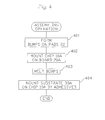
- a Pb-free solder paste or an AuSn eutectic solder paste is stenciled onto the pads 22 of the double-side printed circuit board 20A.
- the optical deflector chip 10A is mounted on the double-side printed circuit board 20A in such a way that the pads 18 of the optical deflector chip 10A are in direct contact with their corresponding pads 22 with the solder paste of the double-side printed circuit board 20A.
- step 303 a reflowing process is carried out at a temperature of 260°C to 310°C in a reflowing furnace.
- the front surface of the optical deflector chip 10A is adhered to the back surface of the double-side printed circuit board 20A.
- step 304 adhesives are coated on either the front surface of the aluminum substrate 30A or the support body 15 of the optical deflector chip 10A. Then, the front surface of the aluminum substrate 30A is mounted on the back surface of the optical deflector chip 10A using the alignment openings 31, so that the front surface of the aluminum substrate 30A is adhered to the back surface, i.e., the support body 15 of the optical deflector chip 10A.
- Au bumps are formed on the pads 22 of the double-side printed circuit board 20A.
- the optical deflector chip 10A is mounted on the double-side printed circuit board 20A in such a way that the pads 18 of the optical deflector chip 10A are in direct contact with their corresponding pads 22 with the Au bumps of the double-side printed circuit board 20A.
- step 403 an ultrasonic and heating bonding operation is performed upon the Au bumps to melt them.
- the front surface of the optical deflector chip 10A is adhered to the back surface of the double-side printed circuit board 20A.
- step 404 adhesives are coated on either the front surface of the aluminum substrate 30A or the support body 15 of the optical deflector chip 10A. Then, the front surface of the aluminum substrate 30A is mounted on the back surface of the optical deflector chip 10A using the alignment openings 31, so that the front surface of the aluminum substrate 30A is adhered to the back surface, i.e., the support body 15 of the optical deflector chip 10A.
- the optical deflector apparatus of Fig. 1 can be reduced in size. Also, since the double-side printed circuit board 20A and the aluminum substrate 30A without TSVs are both inexpensive, the manufacturing cost can be reduced.
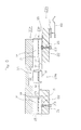
- a front surface of an optical deflector chip 10B is adhered by a so-called flip-chip bonding process to a back surface of a double-side printed circuit board 20B as a first substrate made of inorganic material such as low temperature co-fired ceramic (LTCC), while a back surface of the optical deflector chip 10B is adhered to a front surface of a metal substrate such as an aluminum substrate 30B as a second substrate with no circuit.
- the optical deflector apparatus of Fig. 6 is of a hermetic type where inert gas such as nitrogen gas is introduced to replace the air with it or the inside air is evacuated.
- the optical deflector chip 10B includes frame-shaped sealing electrode patterns 18' and 18" in addition to the elements of the optical deflector chip 10A of Figs. 1 and 2B .
- the materials of the frame-shaped sealing electrode patterns 18' and 18" are the same as those of the pads 18, i.e., plated Au or Cu.
- the frame-shaped sealing electrode patterns 18' are arranged on the front surface of the optical deflector chip 10B at its periphery, i.e., on the front surface of the support body 15, while the frame-shaped sealing electrode patterns 18" are arranged on the back surface of the optical deflector chip 10B at its periphery, i.e., on the back surface of the support body 15.
- the double-side printed circuit board 20B includes interconnections 21' made of Ag or Cu instead of the plated via-structures 21 of the double-side printed circuit board 20A of Figs. 1 and 2C .
- the interconnections 21' connect the pads 22 directly to the electrode terminals 24. Therefore, the pads 23 of Figs. 1 and 2C are not provided.
- the interconnections 21' can be made of refractory metal such as W or Ti.
- the double-side printed circuit board 20B further includes a frame-shaped sealing electrode pattern 22' corresponding to the frame-shaped sealing electrode patterns 18' of the optical deflector chip 10B.
- the materials of the frame-shaped sealing electrode pattern 22' are the same as those of the pads 22.
- the aluminum substrate 30B includes a frame-shaped sealing electrode pattern 32 corresponding to the frame-shaped sealing electrode patterns 18" of the optical deflector chip 10B.
- the materials of the frame-shaped sealing electrode pattern 32 are the same as those of the pads 22, and therefore, the frame-shaped sealing electrode pattern 32 is constructed by a triple structure of Ti (or Cr)/Ni (or Pt)/Au (or Cu) from the aluminum substrate 30B by a plating process, a sputtering process and/or an evaporating process.
- a sealing transparent glass 51 made of borosilicate coated with anti-reflection layers 52a and 52b formed on both sides thereof is provided to seal the opening 20a of the optical deflector apparatus of Fig. 5 .
- a light source for generating incident light to the optical deflector apparatus of Fig. 5 is constructed by a red laser diode, a green laser diode and a blue laser diode
- each of the anti-reflection layers 52a and 52b is configured to reflect a red light component, a green light component and a blue light component.
- step 701 a Pb-free solder paste or an AuSn eutectic solder paste is stenciled onto the pads 22 and the frame-shaped sealing electrode pattern 22' of the double-side printed circuit board 20B and the frame-shaped sealing electrode pattern 32 of the aluminum substrate 30B.
- the optical deflector chip 10B is mounted on the double-side printed circuit board 20B in such a way that the pads 18 and the frame-shaped sealing electrode patterns 18' of the optical deflector chip 10B are in direct contact with their corresponding pads 22 and their corresponding frame-shaped sealing electrode pattern 22' with the solder paste of the double-side printed circuit board 20B. Then, the optical deflector chip 10B is mounted on the aluminum substrate 30B in such a way that the frame-shaped sealing electrode patterns 18" of the optical deflector chip 10B are in direct contact with their corresponding electrode pattern 32 with the solder paste of the aluminum substrate 30B.
- step 703 a reflowing process is carried out at a temperature of 260°C to 310°C in a reflowing furnace.
- the front surface of the optical deflector chip 10B is adhered to the back surface of the double-side printed circuit board 20B and the front surface of the aluminum substrate 30B.
- a sealing transparent glass 51 with anti-reflection layers 52a and 52b is mounted on the front surface of the double-side printed circuit board 20B by a soldering process using a Pb-free solder paste in a nitrogen chamber or a vacuum chamber.
- a nitrogen chamber purging operations are carried out several times to exhaust water vapor, carbon dioxide and the like therefrom.
- the vacuum chamber the pressure is about 0.1 to 0.8 atm.
- step 705 a reflowing process is carried out at a temperature of 260°C in a reflowing furnace.
- the reflowing temperature at step 705 is lower than the reflowing temperature at step 703
- the solder paste between the optical deflector chip 10B and the double-side printed circuit board 20B and the solder paste between the optical deflector chip 10B and the aluminum substrate 30B are never remelted.
- the front surface of the sealing transparent glass 51 is surely adhered to the front surface of the double-side printed circuit board 20B.
- alignment openings 32 can be provided in the corners of the aluminum substrate 30B in the same way as in the first embodiment.
- the optical deflector apparatus of Fig. 5 can be reduced in size. Also, the hermetic optical deflector apparatus can easily be realized without increasing the manufacturing cost.
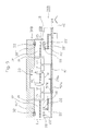
- a mirror 11' is of a rib structure whose thickness is, in this case, the same as the support body 15, and also, a recess 33 opposing the rib structure of the mirror 11' is formed in the aluminum substrate 30A. Therefore, when the mirror 11' with the rib structure is rocked, the mirror 11' with the rib structure never collides with the aluminum substrate 30A. Note that the size of the recess 33 in the traverse direction is smaller than the size of the opening 20a of the double-side printed circuit board 20B in the traverse direction.
- the rib structure of the mirror 11' is operated to effectively suppress the dynamic deformation of the mirror 11' when the mirror 11' is rocking.
- the substrate 30A is made of metal such as aluminum, the recess 33 can easily be formed by a cutting process or the like.
- a mirror 11' is of a rib structure whose thickness is, in this case, the same as the support body 15, and also, a recess 33 opposing the rib structure of the mirror 11' is formed in the aluminum substrate 30B. Therefore, when the mirror 11' with the rib structure is rocked, the mirror 11' with the rib structure never collides with the aluminum substrate 30B.
- the optical deflector chip constitutes a two-dimensional optical deflector where the inner and outer actuators are both torsion-bar type piezoelectric actuators; however, the presently disclosed subject matter can be applied to other two-dimensional optical deflectors. Also, the presently disclosed subject matter can be applied to a one-dimensional optical deflector. Further, the presently disclosed subject matter can be applied to a comb-shaped type electrostatic actuator.
Landscapes
- Engineering & Computer Science (AREA)
- Microelectronics & Electronic Packaging (AREA)
- Physics & Mathematics (AREA)
- General Physics & Mathematics (AREA)
- Optics & Photonics (AREA)
- Computer Hardware Design (AREA)
- Mechanical Light Control Or Optical Switches (AREA)
- Mechanical Optical Scanning Systems (AREA)
- Micromachines (AREA)
Applications Claiming Priority (1)
| Application Number | Priority Date | Filing Date | Title |
|---|---|---|---|
| JP2011215621A JP5989982B2 (ja) | 2011-09-29 | 2011-09-29 | 光偏向器 |
Publications (2)
| Publication Number | Publication Date |
|---|---|
| EP2574973A2 true EP2574973A2 (de) | 2013-04-03 |
| EP2574973A3 EP2574973A3 (de) | 2013-05-22 |
Family
ID=46980683
Family Applications (1)
| Application Number | Title | Priority Date | Filing Date |
|---|---|---|---|
| EP12006417.5A Withdrawn EP2574973A3 (de) | 2011-09-29 | 2012-09-12 | Optische Deflektorvorrichtung mit optischem Deflektor-Chip zwischen zwei Substraten |
Country Status (4)
| Country | Link |
|---|---|
| US (1) | US8937757B2 (de) |
| EP (1) | EP2574973A3 (de) |
| JP (1) | JP5989982B2 (de) |
| CN (1) | CN103076675B (de) |
Cited By (1)
| Publication number | Priority date | Publication date | Assignee | Title |
|---|---|---|---|---|
| EP2962984A1 (de) * | 2014-07-03 | 2016-01-06 | Ricoh Company, Ltd. | Optische deflektorvorrichtung, bilderzeugende vorrichtung, bildanzeigevorrichtung, bewegliche körpervorrichtung und einstellungsverfahren einer optischen deflektorvorrichtung |
Families Citing this family (8)
| Publication number | Priority date | Publication date | Assignee | Title |
|---|---|---|---|---|
| DE102013217146A1 (de) * | 2013-08-28 | 2015-03-05 | Carl Zeiss Smt Gmbh | Optisches Bauelement |
| JP6190703B2 (ja) * | 2013-11-27 | 2017-08-30 | スタンレー電気株式会社 | 光偏向器及び光偏向器チップ |
| JP2016006445A (ja) * | 2014-06-20 | 2016-01-14 | 船井電機株式会社 | 振動ミラーパッケージおよびプロジェクタ |
| CN105719573B (zh) * | 2014-12-03 | 2018-02-23 | 环视先进数字显示无锡有限公司 | 一种复合led铝基玻璃基面板的制造方法 |
| CN106199949B (zh) * | 2016-08-31 | 2018-12-28 | 北京越音速科技有限公司 | 一种压电致动器及变形镜 |
| KR102433236B1 (ko) * | 2016-12-30 | 2022-08-19 | 루미레즈 엘엘씨 | 전기 주조 스텐실 프린팅을 사용하는 led 패키지 |
| JP7302313B2 (ja) * | 2019-06-12 | 2023-07-04 | 住友電気工業株式会社 | 光モジュール |
| WO2025142233A1 (ja) * | 2023-12-25 | 2025-07-03 | パナソニックIpマネジメント株式会社 | 振動モジュールおよび光偏向器 |
Citations (5)
| Publication number | Priority date | Publication date | Assignee | Title |
|---|---|---|---|---|
| US20020051281A1 (en) * | 2000-11-02 | 2002-05-02 | Fujitsu Limited | Galvano-mirror and method of making the same |
| JP2005019966A (ja) | 2003-06-06 | 2005-01-20 | Sanyo Electric Co Ltd | 半導体装置及びその製造方法 |
| JP2008020701A (ja) | 2006-07-13 | 2008-01-31 | Stanley Electric Co Ltd | 2次元光スキャナ、それを用いた光学装置および2次元光スキャナの製造方法 |
| JP2009223165A (ja) | 2008-03-18 | 2009-10-01 | Stanley Electric Co Ltd | 光偏向器 |
| JP2010122480A (ja) | 2008-11-20 | 2010-06-03 | Panasonic Corp | 光学反射素子 |
Family Cites Families (11)
| Publication number | Priority date | Publication date | Assignee | Title |
|---|---|---|---|---|
| JPS60120302A (ja) * | 1983-12-02 | 1985-06-27 | Canon Inc | 光学素子 |
| KR100256162B1 (ko) * | 1994-04-22 | 2000-05-15 | 타테이시 요시오 | 광섬유의 접속 구조, 광섬유의 밀착방법 및 장치, 상기구조, 방법 및 장치를 이용한 광 개폐기 및 광 커넥터 |
| US6873756B2 (en) | 2001-09-07 | 2005-03-29 | Analog Devices, Inc. | Tiling of optical MEMS devices |
| US6920259B2 (en) * | 2003-04-14 | 2005-07-19 | Agilent Technologies, Inc. | Longitudinal electromagnetic latching optical relay |
| JP4390194B2 (ja) * | 2004-03-19 | 2009-12-24 | 株式会社リコー | 偏向ミラー、偏向ミラー製造方法、光書込装置及び画像形成装置 |
| JP2005326620A (ja) | 2004-05-14 | 2005-11-24 | Fujitsu Ltd | マイクロミラー素子 |
| KR20060010419A (ko) * | 2004-07-28 | 2006-02-02 | 삼성전자주식회사 | 구동각도가 향상된 광스캐너 및 이를 적용한 레이저영상투사장치 |
| US7474005B2 (en) * | 2006-05-31 | 2009-01-06 | Alcatel-Lucent Usa Inc. | Microelectronic element chips |
| JP2008020505A (ja) * | 2006-07-11 | 2008-01-31 | Hitachi Metals Ltd | 光スイッチ |
| JP2010008613A (ja) * | 2008-06-25 | 2010-01-14 | Panasonic Electric Works Co Ltd | 半導体機械構造体及びそれを用いた光走査ミラー |
| JP5345090B2 (ja) * | 2010-03-08 | 2013-11-20 | スタンレー電気株式会社 | 光偏向器パッケージ |
-
2011
- 2011-09-29 JP JP2011215621A patent/JP5989982B2/ja active Active
-
2012
- 2012-09-11 US US13/610,119 patent/US8937757B2/en active Active
- 2012-09-12 EP EP12006417.5A patent/EP2574973A3/de not_active Withdrawn
- 2012-09-29 CN CN201210372037.8A patent/CN103076675B/zh active Active
Patent Citations (6)
| Publication number | Priority date | Publication date | Assignee | Title |
|---|---|---|---|---|
| US20020051281A1 (en) * | 2000-11-02 | 2002-05-02 | Fujitsu Limited | Galvano-mirror and method of making the same |
| JP2005019966A (ja) | 2003-06-06 | 2005-01-20 | Sanyo Electric Co Ltd | 半導体装置及びその製造方法 |
| JP2008020701A (ja) | 2006-07-13 | 2008-01-31 | Stanley Electric Co Ltd | 2次元光スキャナ、それを用いた光学装置および2次元光スキャナの製造方法 |
| JP2009223165A (ja) | 2008-03-18 | 2009-10-01 | Stanley Electric Co Ltd | 光偏向器 |
| JP2010122480A (ja) | 2008-11-20 | 2010-06-03 | Panasonic Corp | 光学反射素子 |
| US20110292479A1 (en) | 2008-11-20 | 2011-12-01 | Panasonic Corporation | Optical reflection element |
Cited By (1)
| Publication number | Priority date | Publication date | Assignee | Title |
|---|---|---|---|---|
| EP2962984A1 (de) * | 2014-07-03 | 2016-01-06 | Ricoh Company, Ltd. | Optische deflektorvorrichtung, bilderzeugende vorrichtung, bildanzeigevorrichtung, bewegliche körpervorrichtung und einstellungsverfahren einer optischen deflektorvorrichtung |
Also Published As
| Publication number | Publication date |
|---|---|
| US8937757B2 (en) | 2015-01-20 |
| CN103076675A (zh) | 2013-05-01 |
| JP2013076780A (ja) | 2013-04-25 |
| US20130083381A1 (en) | 2013-04-04 |
| JP5989982B2 (ja) | 2016-09-07 |
| EP2574973A3 (de) | 2013-05-22 |
| CN103076675B (zh) | 2016-04-06 |
Similar Documents
| Publication | Publication Date | Title |
|---|---|---|
| US8937757B2 (en) | Optical deflector apparatus including optical deflector chip sandwhiched by two substrates | |
| JP5500904B2 (ja) | 発光装置の製造方法 | |
| EP1508829B1 (de) | Verformbarer MEMS-Spiegel | |
| WO2008023465A1 (fr) | Dispositif de mécanisme de machine microélectronique et son procédé de fabrication | |
| JP2006221171A (ja) | 光スキャナパッケージ及びその製造方法 | |
| US7141870B2 (en) | Apparatus for micro-electro mechanical system package | |
| US9309043B2 (en) | Optical element storage package, optical filter device, optical module, and electronic apparatus | |
| US20060220223A1 (en) | Reactive nano-layer material for MEMS packaging | |
| JP4475976B2 (ja) | 気密封止パッケージ | |
| JP7541041B2 (ja) | パッケージのためのコンポーネントアレンジメントを製造するための方法、コンポーネントアレンジメントを有するパッケージを製造するための方法、コンポーネントアレンジメント、およびパッケージ | |
| TWI458058B (zh) | 晶片封裝體及其形成方法 | |
| JP2008298205A (ja) | 真空封止装置 | |
| US7098535B2 (en) | Semiconductor package and packaging method using flip-chip bonding technology | |
| KR100886509B1 (ko) | 스크라이브 및 브레이크 처리를 이용한 광학 디바이스의웨이퍼 스케일 패키징 방법 및 디바이스 | |
| CN116105856A (zh) | 红外探测器及其制备方法 | |
| US8204352B2 (en) | Optical apparatus, sealing substrate, and method of manufacturing optical apparatus | |
| JP2008288654A (ja) | 電子デバイス及びその製造方法 | |
| JP2018176421A (ja) | デバイス | |
| JP2008147243A (ja) | 気密封止装置 | |
| JP2014168836A (ja) | 光デバイス封止構造体および封止部品 | |
| US20250210590A1 (en) | Asic integrated mems device with exposed bond pads from bottom attached asic and making the same | |
| US7149023B2 (en) | Optical scanner capable of flip-chip hermetic packaging | |
| WO2016031117A1 (ja) | 電気素子のパッケージ | |
| JP2011191625A (ja) | 光偏向器パッケージ |
Legal Events
| Date | Code | Title | Description |
|---|---|---|---|
| PUAI | Public reference made under article 153(3) epc to a published international application that has entered the european phase |
Free format text: ORIGINAL CODE: 0009012 |
|
| AK | Designated contracting states |
Kind code of ref document: A2 Designated state(s): AL AT BE BG CH CY CZ DE DK EE ES FI FR GB GR HR HU IE IS IT LI LT LU LV MC MK MT NL NO PL PT RO RS SE SI SK SM TR |
|
| AX | Request for extension of the european patent |
Extension state: BA ME |
|
| PUAL | Search report despatched |
Free format text: ORIGINAL CODE: 0009013 |
|
| AK | Designated contracting states |
Kind code of ref document: A3 Designated state(s): AL AT BE BG CH CY CZ DE DK EE ES FI FR GB GR HR HU IE IS IT LI LT LU LV MC MK MT NL NO PL PT RO RS SE SI SK SM TR |
|
| AX | Request for extension of the european patent |
Extension state: BA ME |
|
| RIC1 | Information provided on ipc code assigned before grant |
Ipc: B81B 7/00 20060101ALI20130418BHEP Ipc: G02B 26/08 20060101AFI20130418BHEP |
|
| 17P | Request for examination filed |
Effective date: 20131112 |
|
| RBV | Designated contracting states (corrected) |
Designated state(s): AL AT BE BG CH CY CZ DE DK EE ES FI FR GB GR HR HU IE IS IT LI LT LU LV MC MK MT NL NO PL PT RO RS SE SI SK SM TR |
|
| 17Q | First examination report despatched |
Effective date: 20180827 |
|
| STAA | Information on the status of an ep patent application or granted ep patent |
Free format text: STATUS: THE APPLICATION HAS BEEN WITHDRAWN |
|
| 18W | Application withdrawn |
Effective date: 20181127 |