EP2574978A2 - Appareil de traitement dýinformations - Google Patents
Appareil de traitement dýinformations Download PDFInfo
- Publication number
- EP2574978A2 EP2574978A2 EP12185531A EP12185531A EP2574978A2 EP 2574978 A2 EP2574978 A2 EP 2574978A2 EP 12185531 A EP12185531 A EP 12185531A EP 12185531 A EP12185531 A EP 12185531A EP 2574978 A2 EP2574978 A2 EP 2574978A2
- Authority
- EP
- European Patent Office
- Prior art keywords
- polarizing plate
- extended portion
- frame
- processing apparatus
- information processing
- Prior art date
- Legal status (The legal status is an assumption and is not a legal conclusion. Google has not performed a legal analysis and makes no representation as to the accuracy of the status listed.)
- Withdrawn
Links
Images





Classifications
-
- G—PHYSICS
- G02—OPTICS
- G02F—OPTICAL DEVICES OR ARRANGEMENTS FOR THE CONTROL OF LIGHT BY MODIFICATION OF THE OPTICAL PROPERTIES OF THE MEDIA OF THE ELEMENTS INVOLVED THEREIN; NON-LINEAR OPTICS; FREQUENCY-CHANGING OF LIGHT; OPTICAL LOGIC ELEMENTS; OPTICAL ANALOGUE/DIGITAL CONVERTERS
- G02F1/00—Devices or arrangements for the control of the intensity, colour, phase, polarisation or direction of light arriving from an independent light source, e.g. switching, gating or modulating; Non-linear optics
- G02F1/01—Devices or arrangements for the control of the intensity, colour, phase, polarisation or direction of light arriving from an independent light source, e.g. switching, gating or modulating; Non-linear optics for the control of the intensity, phase, polarisation or colour
- G02F1/13—Devices or arrangements for the control of the intensity, colour, phase, polarisation or direction of light arriving from an independent light source, e.g. switching, gating or modulating; Non-linear optics for the control of the intensity, phase, polarisation or colour based on liquid crystals, e.g. single liquid crystal display cells
- G02F1/133—Constructional arrangements; Operation of liquid crystal cells; Circuit arrangements
- G02F1/1333—Constructional arrangements; Manufacturing methods
- G02F1/133308—Support structures for LCD panels, e.g. frames or bezels
-
- G—PHYSICS
- G09—EDUCATION; CRYPTOGRAPHY; DISPLAY; ADVERTISING; SEALS
- G09F—DISPLAYING; ADVERTISING; SIGNS; LABELS OR NAME-PLATES; SEALS
- G09F9/00—Indicating arrangements for variable information in which the information is built-up on a support by selection or combination of individual elements
-
- G—PHYSICS
- G02—OPTICS
- G02F—OPTICAL DEVICES OR ARRANGEMENTS FOR THE CONTROL OF LIGHT BY MODIFICATION OF THE OPTICAL PROPERTIES OF THE MEDIA OF THE ELEMENTS INVOLVED THEREIN; NON-LINEAR OPTICS; FREQUENCY-CHANGING OF LIGHT; OPTICAL LOGIC ELEMENTS; OPTICAL ANALOGUE/DIGITAL CONVERTERS
- G02F1/00—Devices or arrangements for the control of the intensity, colour, phase, polarisation or direction of light arriving from an independent light source, e.g. switching, gating or modulating; Non-linear optics
- G02F1/01—Devices or arrangements for the control of the intensity, colour, phase, polarisation or direction of light arriving from an independent light source, e.g. switching, gating or modulating; Non-linear optics for the control of the intensity, phase, polarisation or colour
- G02F1/13—Devices or arrangements for the control of the intensity, colour, phase, polarisation or direction of light arriving from an independent light source, e.g. switching, gating or modulating; Non-linear optics for the control of the intensity, phase, polarisation or colour based on liquid crystals, e.g. single liquid crystal display cells
- G02F1/133—Constructional arrangements; Operation of liquid crystal cells; Circuit arrangements
- G02F1/1333—Constructional arrangements; Manufacturing methods
- G02F1/133308—Support structures for LCD panels, e.g. frames or bezels
- G02F1/13332—Front frames
-
- G—PHYSICS
- G02—OPTICS
- G02F—OPTICAL DEVICES OR ARRANGEMENTS FOR THE CONTROL OF LIGHT BY MODIFICATION OF THE OPTICAL PROPERTIES OF THE MEDIA OF THE ELEMENTS INVOLVED THEREIN; NON-LINEAR OPTICS; FREQUENCY-CHANGING OF LIGHT; OPTICAL LOGIC ELEMENTS; OPTICAL ANALOGUE/DIGITAL CONVERTERS
- G02F1/00—Devices or arrangements for the control of the intensity, colour, phase, polarisation or direction of light arriving from an independent light source, e.g. switching, gating or modulating; Non-linear optics
- G02F1/01—Devices or arrangements for the control of the intensity, colour, phase, polarisation or direction of light arriving from an independent light source, e.g. switching, gating or modulating; Non-linear optics for the control of the intensity, phase, polarisation or colour
- G02F1/13—Devices or arrangements for the control of the intensity, colour, phase, polarisation or direction of light arriving from an independent light source, e.g. switching, gating or modulating; Non-linear optics for the control of the intensity, phase, polarisation or colour based on liquid crystals, e.g. single liquid crystal display cells
- G02F1/133—Constructional arrangements; Operation of liquid crystal cells; Circuit arrangements
- G02F1/1333—Constructional arrangements; Manufacturing methods
- G02F1/133308—Support structures for LCD panels, e.g. frames or bezels
- G02F1/133325—Assembling processes
-
- G—PHYSICS
- G02—OPTICS
- G02F—OPTICAL DEVICES OR ARRANGEMENTS FOR THE CONTROL OF LIGHT BY MODIFICATION OF THE OPTICAL PROPERTIES OF THE MEDIA OF THE ELEMENTS INVOLVED THEREIN; NON-LINEAR OPTICS; FREQUENCY-CHANGING OF LIGHT; OPTICAL LOGIC ELEMENTS; OPTICAL ANALOGUE/DIGITAL CONVERTERS
- G02F1/00—Devices or arrangements for the control of the intensity, colour, phase, polarisation or direction of light arriving from an independent light source, e.g. switching, gating or modulating; Non-linear optics
- G02F1/01—Devices or arrangements for the control of the intensity, colour, phase, polarisation or direction of light arriving from an independent light source, e.g. switching, gating or modulating; Non-linear optics for the control of the intensity, phase, polarisation or colour
- G02F1/13—Devices or arrangements for the control of the intensity, colour, phase, polarisation or direction of light arriving from an independent light source, e.g. switching, gating or modulating; Non-linear optics for the control of the intensity, phase, polarisation or colour based on liquid crystals, e.g. single liquid crystal display cells
- G02F1/133—Constructional arrangements; Operation of liquid crystal cells; Circuit arrangements
- G02F1/1333—Constructional arrangements; Manufacturing methods
- G02F1/133308—Support structures for LCD panels, e.g. frames or bezels
- G02F1/133331—Cover glasses
-
- G—PHYSICS
- G02—OPTICS
- G02F—OPTICAL DEVICES OR ARRANGEMENTS FOR THE CONTROL OF LIGHT BY MODIFICATION OF THE OPTICAL PROPERTIES OF THE MEDIA OF THE ELEMENTS INVOLVED THEREIN; NON-LINEAR OPTICS; FREQUENCY-CHANGING OF LIGHT; OPTICAL LOGIC ELEMENTS; OPTICAL ANALOGUE/DIGITAL CONVERTERS
- G02F1/00—Devices or arrangements for the control of the intensity, colour, phase, polarisation or direction of light arriving from an independent light source, e.g. switching, gating or modulating; Non-linear optics
- G02F1/01—Devices or arrangements for the control of the intensity, colour, phase, polarisation or direction of light arriving from an independent light source, e.g. switching, gating or modulating; Non-linear optics for the control of the intensity, phase, polarisation or colour
- G02F1/13—Devices or arrangements for the control of the intensity, colour, phase, polarisation or direction of light arriving from an independent light source, e.g. switching, gating or modulating; Non-linear optics for the control of the intensity, phase, polarisation or colour based on liquid crystals, e.g. single liquid crystal display cells
- G02F1/133—Constructional arrangements; Operation of liquid crystal cells; Circuit arrangements
- G02F1/1333—Constructional arrangements; Manufacturing methods
- G02F1/1335—Structural association of cells with optical devices, e.g. polarisers or reflectors
- G02F1/133528—Polarisers
Definitions
- the present disclosure relates to an information processing apparatus, and more particularly to an information processing apparatus having a display panel and a polarizing plate.
- Embodiments of the present invention can provide an information processing apparatus which includes an electronic device such as a notebook computer and a PDA (Personal Digital Assistant).
- This kind of electronic device has a display panel and a polarizing plate for displaying information such as an image and a character.
- a flush surface structure (structure having an even and smooth surface) like a single plate has been requested for a surface structure of a display part of the electronic device.
- a member e.g., protection plate
- a problem of deterioration e.g., lower visibility or lower luminance
- An embodiment of the present disclosure provides a technique for achieving the optimum flush surface structure without deterioration in the display function.
- an information processing apparatus which includes a rectangular display panel, a polarizing plate covering an entire surface of the display panel, and a frame supporting the display panel, wherein the polarizing plate includes a polarizing plate extended portion extended from at least one side surface of the polarizing plate outward beyond the display panel, and the frame includes a frame extended portion extended from the frame along an extending direction of the polarizing plate extended portion to support the polarizing plate extended portion.
- an utmost surface of the information processing apparatus can be formed of a single plate by an opposite substrate side polarizing plate and the polarizing plate extended portion. Further, the frame extended portion supports the polarizing plate extended portion thereby enabling the polarizing plate extended portion to be inhibited from deformation and the like. Still further, though the opposite substrate side polarizing plate is extended, the display function is not deteriorated. Accordingly, the optimum flush surface structure can be achieved without deterioration in the display function.
- the optimum flush surface structure can be achieved without deterioration in the display function.
- an electronic device such as a notebook computer having a display part is described as an example of an information processing apparatus.
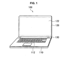
- FIG. 1 is a perspective view illustrating the electronic device 100.
- the electronic device is not limited to the notebook computer but may include a mobile telephone, a PDA, a game machine, an electronic dictionary, a tablet computer and the like.
- the electronic device 100 includes a body side housing 110, a display side housing 120 and a hinge part 130.
- the body side housing 110 and the display side housing 120 are formed of flat plates, respectively, each having the same size as the other.
- the body side housing 110 has an input part 112 accepting a user operation.
- the input part 112 detects the user operation and outputs an electric signal corresponding to the user operation.
- the input part 112 includes a keyboard, a pointing device and the like as illustrated in FIG. 1 . Note that, the input part 112 is not limited to these, but may include a touch panel, for example.
- the display side housing 120 has a display part 122 displaying a various kinds of information.
- the display part 122 includes, for example, a display device such as a liquid crystal display. Note that, a detailed configuration of the display side housing 120 will be described below.
- the hinge part 130 foldably couples the body side housing 110 and the display side housing 120.
- the display side housing 120 turns between an open position illustrated in FIG. 1 and a closed position covering an upper surface of the body side housing 110.
- a configuration of a display side housing according to two comparison examples (first comparison example and second comparison example) will be described with reference to FIG. 2A , FIG. 2B , FIG. 3A and FIG. 3B before describing a configuration of the display side housing 120 according to the present embodiment.
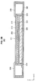
- FIG. 2A is a perspective view illustrating an outline configuration of a display side housing 300 according to the first comparison example.
- FIG. 2B is a cross-sectional view illustrating an outline configuration of the display side housing 300 according to the first comparison example.
- the display side housing 300 according to the first comparison examples includes a liquid crystal display module 310, a housing 340 and an outer periphery bezel frame 350 as illustrated in FIG. 2A and FIG. 2B .
- the liquid crystal display module 310 functions as a display part (liquid crystal display).
- the liquid crystal display module 310 includes a liquid crystal panel 311, a backlight unit 322 and a frame 324.
- the liquid crystal panel 311 includes a drive substrate 312, an opposite substrate 313, a drive substrate side polarizing plate 314 and an opposite substrate side polarizing plate 315. A function and the like of each of the liquid crystal panel 311, the backlight unit 322 and the frame 324 will be described in the present embodiment described below.
- the housing 340 houses and holds the liquid crystal display module 310.
- the outer periphery bezel frame 350 covers the outer periphery of the liquid crystal display module 310.
- the outer periphery bezel frame 350 protrudes from the opposite substrate side polarizing plate 315 of the liquid crystal display module 310 as illustrated in FIG. 2B . Because the outer periphery bezel frame 350 protrudes from the opposite substrate side polarizing plate 315, a difference in level is formed on a front surface of the display side housing 300.
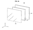
- FIG. 3A is a perspective view illustrating an outline configuration of a display side housing 400 according to the second comparison example.
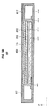
- FIG. 3B is a cross-sectional view illustrating an outline configuration of the display side housing 400 according to the second comparison example.
- the display side housing 400 according to the second comparison example includes a liquid crystal display module 410, a housing 440 and a transparent protection layer 450 as illustrated in FIG. 3A and FIG. 3B . That is, the display side housing 400 has the transparent protection layer 450 instead of the outer periphery bezel frame 350 of the first comparison example.
- the configurations of the liquid crystal display module 410 and the housing 440 are similar to those of the liquid crystal display module 310 and the housing 340 of the first comparison example.
- the transparent protection layer 450 is provided on the liquid crystal display module 410 via an air space.
- the transparent protection layer 450 has a shape larger than that of the opposite substrate 313 and an outer periphery portion of a rear surface of the transparent protection layer 450 is fixed to the housing 440.
- the transparent protection layer 450 is a transparent protection plate or film manufactured from a material such as glass, acrylic and polycarbonate having a certain transmittance.
- a light shielding printed layer 417 is formed in a region of the rear surface of the transparent protection layer 450 corresponding to an outer periphery portion of a liquid crystal display area.
- the light shielding printed layer 417 has a function of hiding an outer periphery portion of the liquid crystal display module 410 and device components and wirings provided on the outer periphery of the liquid crystal display module 410.
- an interface reflection of the outside light or an interface reflection of the backlighting light sometimes occurs at the interface between the air space and the protection layer or at the interface between the air apace and the liquid crystal display module.
- An occurrence of such interface reflection leads to deterioration in visibility of liquid crystal display and lower luminance of the liquid crystal display module 410.
- the electronic device 100 includes a polarizing plate extended portion obtained by extending the opposite substrate side polarizing plate and a frame extended portion obtained by extending the frame corresponding to the polarizing plate extended portion as described below in detail.
- a display side housing 120 according to the present embodiment includes a liquid crystal display module 210 as an example of a display module and a housing 240. Note that, the display side housing 120 according to the present embodiment does not include the above-described outer periphery bezel frame 350 according to the first comparison example and the above-described transparent protection layer 450 according to the second comparison example.
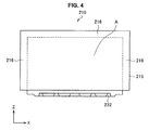
- FIG. 4 is a plan view of the liquid crystal display module 210 according to the present embodiment.
- FIG. 5 is a cross-sectional view of the liquid crystal display module 210.
- the liquid crystal display module 210 includes a liquid crystal panel 211, a backlight unit 222 and a frame 224.
- the liquid crystal panel 211 includes a drive substrate 212, an opposite substrate 213, a drive substrate side polarizing plate 214 and an opposite substrate side polarizing plate 215.
- the drive substrate 212 and the opposite substrate 213 are glass substrates and disposed so as to face each other. Thin film transistors are formed on the drive substrate 212 and color filters are formed on the opposite substrate 213. A liquid crystal material is encapsulated between the drive substrate 212 and the opposite substrate 213.
- the drive substrate 212 and the opposite substrate 213 constitute a rectangular display panel.
- a FPC (Flexible Printed Circuit)/PWB (Printed Wiring Board) mounting region 232 is provided as illustrated in FIG. 4 .
- the FPC/PWB mounting region 232 connects the PWB on which a drive circuit, a backlight drive circuit and an LVDS (Low Voltage Differential Signaling) interface are mounted.
- the reason why the FPC/PWB mounting region 232 is provided at the lower edge of the drive substrate 212 is to achieve thinning of the liquid crystal display module 210.
- the drive substrate side polarizing plate 214 and the opposite substrate side polarizing plate 215 are provided outside the drive substrate 212 and the opposite substrate 213, respectively and each has a function of transmitting light in only one direction but blocking light in other directions by absorption, reflection, scattering or the like.
- the drive substrate side polarizing plate 214 is located below the drive substrate 212 to cover the entire surface of the drive substrate 212.
- the opposite substrate side polarizing plate 215 is located above the opposite substrate 213 to cover the entire surface of the opposite substrate 213.
- the drive substrate side polarizing plate 214 has the same size as the display panel (drive substrate 212, opposite substrate 213) but the opposite substrate side polarizing plate 215 has a larger size than the glass substrate.
- the opposite substrate side polarizing plate 215 has the polarizing plate extended portion 216 extended outward beyond the glass substrate from the side surfaces of the opposite substrate side polarizing plate 215 on three edges other than the lower edge on which the FPC/PWB mounting region 232 is provided. As illustrated in FIG. 4 , the polarizing plate extended portion 216 is located on the outer periphery of a display area A of the liquid crystal display module 210.
- the polarizing plate extended portion 216 is provided on three edges in the above description, but not limited to this, and the polarizing plate extended portion 216 may be provided on only one edge or two edges, for example, or the polarizing plate extended portion 216 may be provided on the all of the four edges.
- the opposite substrate side polarizing plate 215 is laminated such that two sheets of TAC (triacetylcellulose) films sandwich PVA (polyvinyl alcohol).
- TAC triacetylcellulose
- PVA polyvinyl alcohol
- a light shielding printed layer 217 is formed on a rear surface of the opposite substrate side polarizing plate 215. More particularly, the light shielding printed layer 217 is formed on the rear surfaces of the polarizing plate extended portion 216 and the opposite substrate side polarizing plate 215 at the outer periphery of the display area A of the display panel.
- the light shielding printed layer 217 is formed by a black ink or the like to hide an outer periphery portion of the liquid crystal display module 210 and device components and wirings provided on the outer periphery of the liquid crystal display module 210.
- an adhesion layer 218 As an example of a bonding layer is formed.
- the adhesion layer 218 has a function of bonding the opposite substrate side polarizing plate 215 and the polarizing plate extended portion 216 to the opposite substrate 213 and the frame 224 (frame extended portion 225). Because of this, deformation or the like of the opposite substrate side polarizing plate 215 and the polarizing plate extended portion 216 can be effectively inhibited.
- a phase difference film or a liquid crystal film may be provided between the TAC and the light shielding printed layer 217 or the adhesion layer 218.
- the backlight unit 222 irradiates light beams toward the liquid crystal panel 211.
- the backlight unit 222 includes, for example, an LED chip as a light source, a light guide plate, a prism sheet, a diffusion sheet and a reflection sheet.
- the frame 224 supports the backlight unit 222.
- the frame 224 also supports the display panel (drive substrate 212, opposite substrate 213).
- the frame may be a plastic or metal frame, the frame 224 is assumed to be a plastic frame in the present embodiment.
- the frame 224 has the frame extended portion 225 extended from the frame 224 along an extending direction of the polarizing plate extended portion 216.
- the frame extended portion 225 supports the polarizing plate extended portion 216 to inhibit deformation (reinforce intensity) of the thin polarizing plate extended portion 216.
- a profile of the frame extended portion 225 has the same size as a profile of the polarizing plate extended portion 216. Note that, the profile of the frame extended portion 225 may have a larger size than the profile of the polarizing plate extended portion 216.
- the frame extended portion 225 is bonded to the polarizing plate extended portion 216 by the adhesion layer 218.
- the surface of the frame extended portion 225 is to be a bonding plane with the polarizing plate extended portion 216, so that the surface is smooth and flat. Because of this, the polarizing plate extended portion 216 is supported by the frame extended portion 225 in stable condition.
- frame side fixing parts 226 fixing the liquid crystal display module 210 to the housing 240 are formed on the rear surface side of the frame extended portion 225.
- the liquid crystal display module 210 is fixed to the housing 240 by engagement of hooks 226a of the frame side fixing parts 226 with housing side fixing parts 242 of the housing 240. Because of this, the liquid crystal display module 210 can be easily assembled with the housing 240 thereby improving assemblability of the display side housing 120.
- the drive substrate 212 and the opposite substrate 213 are prepared and the display panel is formed by encapsulation of the liquid crystal material between the drive substrate 212 and the opposite substrate 213. Subsequently, the drive substrate side polarizing plate 214 is bonded to the drive substrate 212.
- the display panel is fixed to the frame 224 together with the backlight unit 222.
- the utmost surface of the opposite substrate 213 and the utmost surface of the frame extended portion 225 are flat without any difference in level therebetween.
- the opposite substrate side polarizing plate 215 on which the light shielding printed layer 217 is formed at the outer periphery and the polarizing plate extended portion 216 are bonded onto the opposite substrate 213 and the frame extended portion 225.
- the utmost surface becomes even and the liquid crystal display module 210 like a single plate can be obtained.
- FIG. 6 is a plan view of the display side housing 120 in a state where the liquid crystal display module 210 is fixed to the housing 240.
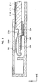
- FIG. 7 is a cross-sectional view along the line A-A in FIG. 6 .
- FIG. 8 is a cross-sectional view along the line B-B in FIG. 6 .
- FIG. 9 is a cross-sectional view along the line C-C in FIG. 6 .
- the housing 240 is provided with the housing side fixing part 242 fixing the liquid crystal display module 210 as illustrated in FIG. 7 .
- the liquid crystal display module 210 and the housing 240 are fixed by engagement of a hook 242a of the housing side fixing part 242 with the hook 226a of the frame side fixing part 226 of the liquid crystal display module 210.
- the wirings and the device components are provided between the frame extended portion 225 having a thickness smaller than a thickness of the liquid crystal display module 210 and the housing 240.
- a wiring space 270 is secured as illustrated in FIG. 7 .
- an antenna wiring 271 and a camera wiring 272 are arranged, for example.
- a camera module 274 as an example of the imaging member is provided as illustrated in FIG. 9 .
- the camera module 274 has an imaging element for taking a picture of a subject, and the like.
- a through hole 225a is provided such as not to disturb image taking by the camera module 247 provided on the rear surface side of the frame extended portion 225.
- the light shielding printed layer 217 having the function of hiding the camera module 274, wirings relevant to the camera module 274 and the like is formed (on a portion where the optical axis does not pass) so as to exclude a portion 217a corresponding to the through hole 225a of the rear surface of the polarizing plate extended portion 216.
- a hole (not shown) may be provided at the portion corresponding to the through hole 225a of the polarizing plate extended portion 216.
- a notch 219 as illustrated in FIG. 10 may be provided instead of the hole. Practically, the notch 219 is also caulked by the acrylic material.
- FIG. 10 is a diagram explanatory of the notch 219 provided on the opposite substrate side polarizing plate 215.
- a lower edge bezel 262 is attached on the side of a lower edge D ( FIG. 6 ) of the display side housing 120 where the polarizing plate extended portion 216 and the frame extended portion 225 are not provided.
- the FPC/PWB mounting region 232 is provided between the lower edge bezel 262 and the housing 240.
- the PWB 234 is connected with the drive substrate 212 via the FPC 236. Note that, in the case where the polarizing plate extended portion 216 and the frame extended portion 225 are provided on the side of the lower edge D of the display side housing 120, the lower edge bezel 262 is unnecessary.
- a rubber cushion 260 as a cushioning material is attached to the outer periphery of the frame extended portion 225 on the utmost outer periphery of the liquid crystal display module 210 as illustrated in FIG. 6 , FIG. 7 and FIG. 9 .
- the rubber cushion 260 is illustrated as to protrude from the frame extended portion 225, but not limited to this, and the rubber cushion 260 may not protrude from the frame extended portion 225.
- the opposite substrate side polarizing plate 215 and the polarizing plate extended portion 216 form the utmost surface of the display side housing 120.
- This is unlike the first comparison example where the outer periphery bezel frame 350 forms the utmost surface of the display side housing 300 or unlike the second comparison example where the transparent protection layer 450 forms the utmost surface of the display side housing 400.
- the opposite substrate side polarizing plate 215 of the electronic device 100 has the polarizing plate extended portion 216 extended from at least one side surface of the opposite substrate side polarizing plate 215 outward beyond the opposite substrate 213.
- the frame 224 has the frame extended portion 225 extended from the frame 224 along the extending direction of the polarizing plate extended portion 216 to support the polarizing plate extended portion 216.
- the opposite substrate side polarizing plate 215 and the polarizing plate extended portion 216 can form the utmost surface of the display side housing 120 by a single plate. Further, the frame extended portion 225 supports the polarizing plate extended portion 216 thereby inhibiting deformation and the like of the polarizing plate extended portion 216. Still further, the polarizing plate extended portion 216 does not deteriorate the display function. As a result, according to the present embodiment, the optimum flush surface structure can be achieved without deterioration in the display function.
- the thinner and more lightweight flush surface structure can be achieved in comparison with the first comparison example and the second comparison example because the outer periphery bezel frame 350 in the first comparison example and the transparent protection layer 450 in the second comparison example become unnecessary. Further, deterioration in the display function such as lower visibility of the liquid crystal display and lower luminance of the liquid crystal display module caused by the transparent protection layer 450 can be inhibited. In addition, the increase in the assembly cost and the increase in the infrastructure cost due to the additional manufacturing process are inhibited by not using the outer periphery bezel frame 350 and the transparent protection layer 450.
- an appearance close to an unlit state and a light blocking effect of the display area of the liquid crystal display module 210 can be ensured by providing the light shielding printed layer 217 on the rear surface side of the polarizing plate extended portion 216. Still further, it becomes easy to assemble the liquid crystal display module 210 with the housing 240 and it becomes easy to rework the structure by providing the frame side fixing parts 226. Still further, the notebook computer can be thinned because the space for housing the wirings of the surrounding members such as the antenna wiring is provided on the rear surface of the frame extended portion 225 of the backlight unit.
- the display module includes the liquid crystal display module (liquid crystal display), but not limited to this.
- the display module may include an organic EL display, for example as long as having the display panel and the polarizing plate.
Landscapes
- Physics & Mathematics (AREA)
- Nonlinear Science (AREA)
- General Physics & Mathematics (AREA)
- Mathematical Physics (AREA)
- Chemical & Material Sciences (AREA)
- Crystallography & Structural Chemistry (AREA)
- Optics & Photonics (AREA)
- Engineering & Computer Science (AREA)
- Theoretical Computer Science (AREA)
- Liquid Crystal (AREA)
- Devices For Indicating Variable Information By Combining Individual Elements (AREA)
Applications Claiming Priority (1)
| Application Number | Priority Date | Filing Date | Title |
|---|---|---|---|
| JP2011211862A JP2013073009A (ja) | 2011-09-28 | 2011-09-28 | 情報処理装置 |
Publications (2)
| Publication Number | Publication Date |
|---|---|
| EP2574978A2 true EP2574978A2 (fr) | 2013-04-03 |
| EP2574978A3 EP2574978A3 (fr) | 2013-07-03 |
Family
ID=47225935
Family Applications (1)
| Application Number | Title | Priority Date | Filing Date |
|---|---|---|---|
| EP12185531.6A Withdrawn EP2574978A3 (fr) | 2011-09-28 | 2012-09-21 | Appareil de traitement dýinformations |
Country Status (6)
| Country | Link |
|---|---|
| US (1) | US8958033B2 (fr) |
| EP (1) | EP2574978A3 (fr) |
| JP (1) | JP2013073009A (fr) |
| KR (1) | KR20150127868A (fr) |
| CN (2) | CN103064204A (fr) |
| TW (1) | TW201317674A (fr) |
Families Citing this family (19)
| Publication number | Priority date | Publication date | Assignee | Title |
|---|---|---|---|---|
| WO2012002019A1 (fr) * | 2010-06-29 | 2012-01-05 | シャープ株式会社 | Dispositif d'affichage |
| JP2013073009A (ja) * | 2011-09-28 | 2013-04-22 | Sony Corp | 情報処理装置 |
| TWI513077B (zh) * | 2013-12-11 | 2015-12-11 | Ultimate Image Corp | 有機發光二極體照明裝置 |
| US9513751B2 (en) * | 2014-06-27 | 2016-12-06 | Microsoft Technology Licensing, Llc | Large-format display assembly |
| KR20160008675A (ko) * | 2014-07-14 | 2016-01-25 | 삼성디스플레이 주식회사 | 표시장치 |
| JP6291397B2 (ja) | 2014-10-28 | 2018-03-14 | 株式会社ジャパンディスプレイ | 液晶表示装置 |
| CN106154597A (zh) | 2015-04-21 | 2016-11-23 | 小米科技有限责任公司 | 移动设备 |
| JP6675906B2 (ja) * | 2016-03-30 | 2020-04-08 | 三菱電機株式会社 | 液晶表示装置 |
| CN106226947A (zh) * | 2016-09-20 | 2016-12-14 | 南昌欧菲显示科技有限公司 | 一体色显示屏 |
| CN107526203A (zh) * | 2017-03-14 | 2017-12-29 | 惠科股份有限公司 | 一种显示装置及其制程 |
| JP6159902B1 (ja) * | 2017-03-15 | 2017-07-05 | 京セラ株式会社 | 電子機器 |
| JP6177472B1 (ja) * | 2017-03-15 | 2017-08-09 | 京セラ株式会社 | 電子機器 |
| JP6162915B1 (ja) * | 2017-03-15 | 2017-07-12 | 京セラ株式会社 | 電子機器 |
| CN107167963A (zh) * | 2017-06-21 | 2017-09-15 | 苏州佳世达电通有限公司 | 显示装置 |
| JP6961310B2 (ja) * | 2018-01-10 | 2021-11-05 | アルパイン株式会社 | 車載用表示装置 |
| JP2019133098A (ja) * | 2018-02-02 | 2019-08-08 | シャープ株式会社 | 表示デバイス |
| JP2019158956A (ja) * | 2018-03-08 | 2019-09-19 | シャープ株式会社 | 表示デバイス |
| WO2019237274A1 (fr) * | 2018-06-13 | 2019-12-19 | Oppo广东移动通信有限公司 | Ensemble dispositif d'affichage destiné à un dispositif électronique et dispositif électronique |
| TWI876447B (zh) * | 2023-07-28 | 2025-03-11 | 技嘉科技股份有限公司 | 顯示裝置及撓性框體 |
Family Cites Families (9)
| Publication number | Priority date | Publication date | Assignee | Title |
|---|---|---|---|---|
| US5737047A (en) * | 1995-03-27 | 1998-04-07 | Casio Computer Co., Ltd. | Color liquid crystal display device with optical axes of retardation polarization plates set in an opposite direction of twist direction of LC molecules |
| JP4483833B2 (ja) | 2005-09-22 | 2010-06-16 | エプソンイメージングデバイス株式会社 | 電気光学装置、電子機器、保護部材、保護部材の製造方法 |
| KR20080073910A (ko) | 2007-02-07 | 2008-08-12 | 삼성전자주식회사 | 액정 표시 장치 |
| JP4973311B2 (ja) | 2007-05-16 | 2012-07-11 | ソニー株式会社 | 電子機器 |
| JP5026163B2 (ja) | 2007-06-26 | 2012-09-12 | セイコーインスツル株式会社 | 電子機器 |
| JP2009036842A (ja) | 2007-07-31 | 2009-02-19 | Nec Lcd Technologies Ltd | 表示装置 |
| JP4920646B2 (ja) * | 2008-09-04 | 2012-04-18 | 株式会社 日立ディスプレイズ | 液晶表示装置 |
| KR20100039013A (ko) * | 2008-10-07 | 2010-04-15 | 삼성전자주식회사 | 표시 장치와 상기 표시 장치의 제조방법 |
| JP2013073009A (ja) * | 2011-09-28 | 2013-04-22 | Sony Corp | 情報処理装置 |
-
2011
- 2011-09-28 JP JP2011211862A patent/JP2013073009A/ja not_active Withdrawn
-
2012
- 2012-09-12 US US13/611,782 patent/US8958033B2/en not_active Expired - Fee Related
- 2012-09-17 KR KR1020120102565A patent/KR20150127868A/ko not_active Withdrawn
- 2012-09-18 TW TW101134149A patent/TW201317674A/zh unknown
- 2012-09-21 CN CN2012103556123A patent/CN103064204A/zh active Pending
- 2012-09-21 CN CN2012204847140U patent/CN202929522U/zh not_active Expired - Fee Related
- 2012-09-21 EP EP12185531.6A patent/EP2574978A3/fr not_active Withdrawn
Non-Patent Citations (1)
| Title |
|---|
| None |
Also Published As
| Publication number | Publication date |
|---|---|
| US8958033B2 (en) | 2015-02-17 |
| US20130077017A1 (en) | 2013-03-28 |
| EP2574978A3 (fr) | 2013-07-03 |
| CN202929522U (zh) | 2013-05-08 |
| CN103064204A (zh) | 2013-04-24 |
| JP2013073009A (ja) | 2013-04-22 |
| TW201317674A (zh) | 2013-05-01 |
| KR20150127868A (ko) | 2015-11-18 |
Similar Documents
| Publication | Publication Date | Title |
|---|---|---|
| US8958033B2 (en) | Information processing apparatus | |
| US9910306B2 (en) | Display device and set electronic device including the display device | |
| EP2527911B1 (fr) | Écran | |
| US20110317087A1 (en) | Display module | |
| US20140133174A1 (en) | Displays and Display Chassis Structures | |
| US20130335670A1 (en) | Planar display device | |
| GB2486931A (en) | Portable computer having integral camera imaging via display screen opening | |
| WO2014035769A1 (fr) | Procédé pour concevoir le verre de couverture de module de dispositif d'affichage à cristaux liquides (lcd) à couverture totale intégré | |
| CN104063084B (zh) | 触控显示装置 | |
| US20120169633A1 (en) | Touch-sensitive display device | |
| US9885899B2 (en) | Display device | |
| KR20150066615A (ko) | 액정 표시 장치 | |
| JP6443342B2 (ja) | 表示装置 | |
| WO2014175172A1 (fr) | Dispositif d'affichage à cristaux liquides | |
| US10095333B2 (en) | Touch apparatus | |
| KR101463683B1 (ko) | 액정표시장치 | |
| CN112965291B (zh) | 一种显示装置及其背光模组 | |
| CN116699891B (zh) | 显示屏及电子设备 | |
| US10330859B2 (en) | Display device and backlight module | |
| US9164304B2 (en) | Liquid crystal display assembly and electronic device | |
| US11315915B2 (en) | Display device | |
| CN112700728A (zh) | 显示模组及电子设备 | |
| KR20170015727A (ko) | 표시장치 | |
| US9140925B2 (en) | Display with reduced border | |
| TWI386721B (zh) | 液晶顯示裝置 |
Legal Events
| Date | Code | Title | Description |
|---|---|---|---|
| PUAI | Public reference made under article 153(3) epc to a published international application that has entered the european phase |
Free format text: ORIGINAL CODE: 0009012 |
|
| 17P | Request for examination filed |
Effective date: 20120928 |
|
| AK | Designated contracting states |
Kind code of ref document: A2 Designated state(s): AL AT BE BG CH CY CZ DE DK EE ES FI FR GB GR HR HU IE IS IT LI LT LU LV MC MK MT NL NO PL PT RO RS SE SI SK SM TR |
|
| AX | Request for extension of the european patent |
Extension state: BA ME |
|
| PUAL | Search report despatched |
Free format text: ORIGINAL CODE: 0009013 |
|
| AK | Designated contracting states |
Kind code of ref document: A3 Designated state(s): AL AT BE BG CH CY CZ DE DK EE ES FI FR GB GR HR HU IE IS IT LI LT LU LV MC MK MT NL NO PL PT RO RS SE SI SK SM TR |
|
| AX | Request for extension of the european patent |
Extension state: BA ME |
|
| RIC1 | Information provided on ipc code assigned before grant |
Ipc: G02F 1/1335 20060101ALI20130524BHEP Ipc: G02F 1/1333 20060101AFI20130524BHEP |
|
| 17Q | First examination report despatched |
Effective date: 20140606 |
|
| STAA | Information on the status of an ep patent application or granted ep patent |
Free format text: STATUS: THE APPLICATION IS DEEMED TO BE WITHDRAWN |
|
| 18D | Application deemed to be withdrawn |
Effective date: 20150623 |