EP2575169A2 - Joining aid for a power module - Google Patents
Joining aid for a power module Download PDFInfo
- Publication number
- EP2575169A2 EP2575169A2 EP12185297A EP12185297A EP2575169A2 EP 2575169 A2 EP2575169 A2 EP 2575169A2 EP 12185297 A EP12185297 A EP 12185297A EP 12185297 A EP12185297 A EP 12185297A EP 2575169 A2 EP2575169 A2 EP 2575169A2
- Authority
- EP
- European Patent Office
- Prior art keywords
- metal
- layer
- ceramic composite
- composite material
- material layer
- Prior art date
- Legal status (The legal status is an assumption and is not a legal conclusion. Google has not performed a legal analysis and makes no representation as to the accuracy of the status listed.)
- Withdrawn
Links
Images
Classifications
-
- H—ELECTRICITY
- H10—SEMICONDUCTOR DEVICES; ELECTRIC SOLID-STATE DEVICES NOT OTHERWISE PROVIDED FOR
- H10W—GENERIC PACKAGES, INTERCONNECTIONS, CONNECTORS OR OTHER CONSTRUCTIONAL DETAILS OF DEVICES COVERED BY CLASS H10
- H10W70/00—Package substrates; Interposers; Redistribution layers [RDL]
- H10W70/20—Conductive package substrates serving as an interconnection, e.g. metal plates
-
- H—ELECTRICITY
- H10—SEMICONDUCTOR DEVICES; ELECTRIC SOLID-STATE DEVICES NOT OTHERWISE PROVIDED FOR
- H10W—GENERIC PACKAGES, INTERCONNECTIONS, CONNECTORS OR OTHER CONSTRUCTIONAL DETAILS OF DEVICES COVERED BY CLASS H10
- H10W70/00—Package substrates; Interposers; Redistribution layers [RDL]
- H10W70/40—Leadframes
- H10W70/411—Chip-supporting parts, e.g. die pads
- H10W70/417—Bonding materials between chips and die pads
-
- H—ELECTRICITY
- H10—SEMICONDUCTOR DEVICES; ELECTRIC SOLID-STATE DEVICES NOT OTHERWISE PROVIDED FOR
- H10W—GENERIC PACKAGES, INTERCONNECTIONS, CONNECTORS OR OTHER CONSTRUCTIONAL DETAILS OF DEVICES COVERED BY CLASS H10
- H10W72/00—Interconnections or connectors in packages
- H10W72/30—Die-attach connectors
-
- H—ELECTRICITY
- H10—SEMICONDUCTOR DEVICES; ELECTRIC SOLID-STATE DEVICES NOT OTHERWISE PROVIDED FOR
- H10W—GENERIC PACKAGES, INTERCONNECTIONS, CONNECTORS OR OTHER CONSTRUCTIONAL DETAILS OF DEVICES COVERED BY CLASS H10
- H10W72/00—Interconnections or connectors in packages
- H10W72/071—Connecting or disconnecting
- H10W72/073—Connecting or disconnecting of die-attach connectors
- H10W72/07331—Connecting techniques
- H10W72/07336—Soldering or alloying
-
- H—ELECTRICITY
- H10—SEMICONDUCTOR DEVICES; ELECTRIC SOLID-STATE DEVICES NOT OTHERWISE PROVIDED FOR
- H10W—GENERIC PACKAGES, INTERCONNECTIONS, CONNECTORS OR OTHER CONSTRUCTIONAL DETAILS OF DEVICES COVERED BY CLASS H10
- H10W90/00—Package configurations
- H10W90/701—Package configurations characterised by the relative positions of pads or connectors relative to package parts
- H10W90/731—Package configurations characterised by the relative positions of pads or connectors relative to package parts of die-attach connectors
- H10W90/734—Package configurations characterised by the relative positions of pads or connectors relative to package parts of die-attach connectors between a chip and a stacked insulating package substrate, interposer or RDL
Definitions
- a circuit arrangement comprising a circuit arrangement which comprises at least one power semiconductor and at least the metallic line layer of a circuit carrier, wherein arranged between the power semiconductor and the circuit carrier in material-locking contact with both a metal-ceramic composite material layer with a continuous metal content of ⁇ 20% is.
- the term "power semiconductor” is understood in particular a semiconducting chip, which has the task of rectifying currents (diode) or switch (transistor).
- the power semiconductor preferably consists essentially of silicon, silicon carbide or gallium nitride.
- circuit carrier is understood in particular to mean a layer structure which consists of at least one metallic conductor layer and one insulation layer.
- the conductor layer consists essentially of a metal such as copper, aluminum or their mixtures or alloys, the insulating layer of ceramics or polymers.
- metal-ceramic composite material layer is understood in particular to mean a layer in which a porous ceramic layer is first produced from a suitable precursor material such as a powder or a green compact and then the pores are infiltrated by metal.
- a suitable precursor material such as a powder or a green compact
- the metal / ceramic ratio along the composite layer can be substantially constant.
- an expansion coefficient of the composite material layer can be adjusted in an advantageous manner. For example, the setting of an expansion coefficient, which lies between that of the respective joining partner, is preferred.
- the term "in cohesive contact with both” is understood in particular to mean that the metal-ceramic composite material layer is in direct contact, at least in partial areas, preferably flatly with both the power semiconductor and the circuit carrier, so that not only the mechanical integrity but also a heat How electrical charge transport is possible.
- An embodiment of the metal-ceramic composite material layer is preferably provided in which it has a planar metallization at least in the area of contact with a joining partner. This favors a cohesive connection to the joining partners. More preferably, the metallization layer is selected from the metal contained proportionately in the metal-ceramic composite material layer.
- the connecting layer is preferably made of a solderable, sinterable and / or sintered material.
- continuous metal content is understood to mean, in particular, that in the metal-ceramic composite material layer along the direction from the power semiconductor to the circuit carrier, the metal content is never lower than the stated percentage (in% by volume to% by volume of the layer; following for the entire text) amounts to. It has been found that a continuous minimum metal content of ⁇ 20% is necessary in order not to impair the functioning of the circuit arrangement. Preferably, the continuous metal content is ⁇ 30%.
- the thermal expansion difference of the metal-ceramic composite layer and the thermal expansion of at least the portions of each of the circuit carrier and the power semiconductor adjacent to the metal-ceramic composite layer is ⁇ 14 * 10 -6 / K, preferably ⁇ 12 * 10 -6 / K, more preferably ⁇ 10 * 10 -6 / K, and most preferably ⁇ 8 * 10 -6 / K.
- the metal content in the metal-ceramic composite layer (based on the entire layer) is from ⁇ 30% to ⁇ 70%. This has proven to be advantageous in practice, in particular with regard to the setting of a suitable expansion coefficient, as well as with respect to a very good electrical and thermal conductivity.
- the metal content in the metal-ceramic composite layer (based on the entire layer) is from ⁇ 40% to ⁇ 60%, more preferably about 50%.
- the metal content of the metal-ceramic composite layer increases continuously or in a stepped manner in the direction of the circuit carrier. This has proved to be advantageous in many applications, since in this way, for example, two joining partners with different coefficients of expansion can be suitably matched to one another in terms of their thermal expansion behavior. According to the invention, thermally induced stresses in the joining partners are avoided, at least significantly reduced.
- the gradient may be in the metal-ceramic composite layer i.a. can be produced by varying the number and / or the size of the pores along the layer during the production of the ceramic layer so that the metal content during the infiltration with metal is not uniform along the composite layer.
- the ceramic component of the metal-ceramic composite material layer aluminum oxide, aluminum nitride, copper carbide, silicon nitride and / or silicon carbide are provided.
- Such materials can be produced in a simple form as a sintered molded body, which can then be infiltrated with a metal, for example. It is also conceivable deviating oxide ceramics or non-oxide ceramics based on carbides, nitrides or borides.
- the metal portion of the metal-ceramic composite material layer silver, copper, aluminum or their mixtures and alloys.
- Such materials are easy to process and are particularly suitable for infiltrating into prepared sintered shaped bodies for forming a metal-ceramic composite material layer.
- the present invention also relates to a composite layer for joining electronic and / or electrical components as joining partners, comprising at least one carrier film and a layer arrangement arranged thereon comprising a metal-ceramic composite material layer, and a metallization layer arranged on the metal-ceramic composite material layer and / or tie layer.
- a composite layer for joining electronic and / or electrical components as joining partners comprising at least one carrier film and a layer arrangement arranged thereon comprising a metal-ceramic composite material layer, and a metallization layer arranged on the metal-ceramic composite material layer and / or tie layer.
- the carrier film is preferably designed to be adhesively adhesive to the layer arrangement and serves primarily as a transport and handling aid and as protection for the layer arrangement against contamination.
- the carrier film may be provided on one side or on both sides adhering to the layer arrangement.
- the layer arrangement When producing, for example, a circuit arrangement according to the invention, the layer arrangement can be detached from the carrier foil in a simple manner. Thereupon, the layer arrangement for connecting electronic and / or electrical components can be arranged as a joining partner between them.
- the layer composite according to the invention can be used as a connecting element such as an electronic or electrical component in the manufacturing process.
- a layer composite according to the invention may contain further ceramic, metal or metal-ceramic composite material layers. Particularly preferred is an embodiment in which a metallization layer and / or a connection layer are provided on both sides of the metal-ceramic composite material layer.
- the present invention also relates to a power module comprising a circuit arrangement according to the invention and / or a layer composite according to the invention.
- the term "power module” is understood in particular to mean a circuit carrier with power semiconductors connected thereto and a housing.
- the housing is formed from a metal or from a circuit carrier and / or the power semiconductor at least partially enclosing molding compound.
- the metal-ceramic composite material layer can be connected or applied to the power semiconductor and / or the circuit carrier in the following manner: soft and hard soldering, diffusion soldering, sintering, bonding, welding, infiltration.
- the metal-ceramic composite material layer can be provided with a metallization in the area of contact to a joining partner, for example to the power semiconductor or to the circuit carrier.
- a bonding layer can be applied between the metal-ceramic composite material layer and one of the joining partners to form a cohesive contact, in particular a solderable, sinterable and / or sintered bonding layer.
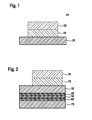
- Fig.1 shows a schematic fragmentary sectional view of a power module 1.
- the power module comprises a circuit arrangement according to a first embodiment of the invention consisting of a power semiconductor 20 and a punched grid 30, which constitutes the circuit carrier. Between the power semiconductor 20 and the punched grid / circuit carrier 30, the metal-ceramic composite material layer 10 is arranged so that it has in material-locking contact both to the power semiconductor 20 and the circuit substrate 30.
- both the thermo-mechanical differences resulting from the different materials of the power semiconductor 20 (semiconductor material such as silicon, etc.) and the circuit carrier 30 (which essentially consists of metal) largely compensate each other or none lead only insignificantly life-like efficiency losses of the power module 1.
- Fig. 2 a schematic partial sectional view of a power module according to a second embodiment of the invention.
- Components associated with the Power module off Fig. 1 are identical, are provided with the same reference numerals and will not be discussed again.
- the power module off Fig. 2 is different from that Fig. 1 in that a circuit carrier is formed, in which further MMC metal and ceramic layers are provided. Specifically, these are an intermediate layer 40 made of a metal-ceramic composite material layer, a ceramic layer 50, a further intermediate layer 60 made of a metal-ceramic composite material layer and a metal layer 70.
Landscapes
- Cooling Or The Like Of Semiconductors Or Solid State Devices (AREA)
- Die Bonding (AREA)
Abstract
Description
Leistungsmodule, Leistungseinrichtungen sowie Verfahren zu deren Herstellung sind aus dem Stand der Technik bekannt und deren Einsatz wird inzwischen aufgrund der Energiesparpotenziale häufig als Antwort auf die globale Klimaerwärmung angesehen.Power modules, power devices and methods for their production are known from the prior art and their use is now considered due to the energy savings potential often in response to global warming.
Bei konventionellen Leistungsmodulen und den darin enthaltenen Schaltungsanordnungen ist insbesondere der Unterschied der thermischen Ausdehnungskoeffizienten zwischen den einzelnen Bestandteilen des Leistungsmoduls aufgrund versagensrelevanter thermischer Spannungen im Bauteil problematisch.In the case of conventional power modules and the circuit arrangements contained therein, in particular the difference of the thermal expansion coefficients between the individual components of the power module is problematic due to failure-relevant thermal stresses in the component.
Somit ist es eine Aufgabe der vorliegenden Erfindung, eine verbesserte Schaltungsanordnung bereitzustellen. Diese Aufgabe wird durch den Anspruch 1 der vorliegenden Erfindung gelöst. Demgemäß wird ein Schaltungsanordnung vorgeschlagen, umfassend eine Schaltungsanordnung, die mindestens einen Leistungshalbleiter sowie zumindest die metallischen Leitungsschicht eines Schaltungsträgers umfasst, wobei zwischen dem Leistungshalbleiter und dem Schaltungsträger in stoffschlüssigem Kontakt mit beiden eine Metall-Keramik-Verbundwerkstoffschicht mit einem durchgehenden Metallanteil von ≥20% angeordnet ist.Thus, it is an object of the present invention to provide an improved circuit arrangement. This object is solved by claim 1 of the present invention. Accordingly, a circuit arrangement is proposed, comprising a circuit arrangement which comprises at least one power semiconductor and at least the metallic line layer of a circuit carrier, wherein arranged between the power semiconductor and the circuit carrier in material-locking contact with both a metal-ceramic composite material layer with a continuous metal content of ≥20% is.
Überraschend hat sich herausgestellt, dass so die Lebensdauer und die Leistungsfähigkeit der Schaltungsanordnung bei vielen Anwendungen deutlich erhöht werden kann ohne dass die Funktionsweise der Schaltungsanordnung mehr als unwesentlich eingeschränkt wird.Surprisingly, it has been found that the life and performance of the circuit can be significantly increased in many applications without the functioning of the circuit is more than insignificantly limited.
Unter dem Term "Leistungshalbleiter" wird insbesondere eine halbleitender Chip verstanden, der die Aufgabe hat Ströme gleichzurichten (Diode) oder zu schalten (Transistor). Bevorzugt besteht der Leistungshalbleiter im wesentlichen aus Silizium, Siliziumcarbid oder Galliumnitrid.The term "power semiconductor" is understood in particular a semiconducting chip, which has the task of rectifying currents (diode) or switch (transistor). The power semiconductor preferably consists essentially of silicon, silicon carbide or gallium nitride.
Unter dem Term "Schaltungsträger" wird insbesondere ein Lagenaufbau verstanden, der aus mindestens einer metallischen Leitungsschicht und einer Isolationsschicht besteht. Bevorzugt besteht die Leitungsschicht im wesentlichen aus einem Metall wie Kupfer, Aluminium bzw. deren Mischungen oder Legierungen, die Isolationsschicht aus Keramiken oder Polymeren.The term "circuit carrier" is understood in particular to mean a layer structure which consists of at least one metallic conductor layer and one insulation layer. Preferably, the conductor layer consists essentially of a metal such as copper, aluminum or their mixtures or alloys, the insulating layer of ceramics or polymers.
Unter dem Term "Metall-Keramik-Verbundwerkstoffschicht" wird insbesondere eine Schicht verstanden, bei der zunächst aus einem geeigneten Vorläufermaterial wie ein Pulver oder ein Grünling eine poröse Keramikschicht hergestellt wird und anschließend die Poren durch Metall infiltriert werden. Dabei kann das Metall/Keramik-Verhältnis entlang der Verbundwerkstoffschicht im wesentlichen konstant sein. Durch die Wahl des Metall/Keramik-Verhältnis kann in vorteilhafter Weise ein Ausdehnungskoeffizient der Verbundwerkstoffschicht eingestellt werden. Beispielsweise ist die Einstellung eines Ausdehnungskoeffizienten, welcher zwischen dem der jeweiligen Fügepartner liegt, bevorzugt einzustellen.The term "metal-ceramic composite material layer" is understood in particular to mean a layer in which a porous ceramic layer is first produced from a suitable precursor material such as a powder or a green compact and then the pores are infiltrated by metal. In this case, the metal / ceramic ratio along the composite layer can be substantially constant. By choosing the metal / ceramic ratio, an expansion coefficient of the composite material layer can be adjusted in an advantageous manner. For example, the setting of an expansion coefficient, which lies between that of the respective joining partner, is preferred.
Unter dem Begriff "in stoffschlüssigem Kontakt mit beiden" wird insbesondere verstanden, dass die Metall-Keramik-Verbundwerkstoffschicht zumindest in Teilbereichen, vorzugsweise flächig abschließend sowohl mit dem Leistungshalbleiter wie dem Schaltungsträger in direktem Kontakt steht, so dass neben der mechanischen Integrität sowohl ein Wärme- wie elektrischer Ladungstransport möglich ist. Bevorzugte ist eine Ausführung der Metall-Keramik-Verbundwerkstoffschicht vorgesehen, bei welcher diese zumindest im Kontaktbereich zu einem Fügepartner eine flächige Metallisierung aufweist. Dadurch wird eine stoffschlüssige Anbindung an die Fügepartner begünstigt. Weiter bevorzugt ist die Metallisierungsschicht aus dem anteilig in der Metall-Keramik-Verbundwerkstoffschicht enthaltenen Metall ausgewählt.The term "in cohesive contact with both" is understood in particular to mean that the metal-ceramic composite material layer is in direct contact, at least in partial areas, preferably flatly with both the power semiconductor and the circuit carrier, so that not only the mechanical integrity but also a heat How electrical charge transport is possible. An embodiment of the metal-ceramic composite material layer is preferably provided in which it has a planar metallization at least in the area of contact with a joining partner. This favors a cohesive connection to the joining partners. More preferably, the metallization layer is selected from the metal contained proportionately in the metal-ceramic composite material layer.
Zusätzlich vorteilhaft ist das Vorsehen einer Verbindungsschicht im Kontaktbereich zwischen der Metall-Keramik-Verbundwerkstoffschicht und einem Fügepartner. Bevorzugt ist die Verbindungsschicht aus einem lötbarem, sinterbarem und/oder gesintertem Material.Additionally advantageous is the provision of a connecting layer in the contact region between the metal-ceramic composite material layer and a joining partner. The connecting layer is preferably made of a solderable, sinterable and / or sintered material.
Unter dem Term "durchgehender Metallanteil" wird insbesondere verstanden, dass in der Metall-Keramik-Verbundwerkstoffschicht entlang der Richtung vom Leistungshalbleiter zum Schaltungsträger der Metallanteil niemals geringer als der angegebene Prozentsatz (in Vol-% zu Vol-% der Schicht, dies gilt auch im folgenden für den gesamten Text) beträgt. Es hat sich herausgestellt, dass ein durchgehender Mindestmetallanteil von ≥20% notwendig ist, um die Funktionsweise der Schaltungsanordnung nicht zu beeinträchtigen. Bevorzugt beträgt der durchgehende Metallanteil ≥30%.The term "continuous metal content" is understood to mean, in particular, that in the metal-ceramic composite material layer along the direction from the power semiconductor to the circuit carrier, the metal content is never lower than the stated percentage (in% by volume to% by volume of the layer; following for the entire text) amounts to. It has been found that a continuous minimum metal content of ≥20% is necessary in order not to impair the functioning of the circuit arrangement. Preferably, the continuous metal content is ≥30%.
Gemäß einer bevorzugten Ausführungsform der vorliegenden Erfindung beträgt der Unterschied der thermischen Ausdehnung der Metall-Keramik-Verbundwerkstoffschicht und der thermischen Ausdehnung zumindest der Bereiche sowohl des Schaltungsträgers und des Leistungshalbleiters, die der Metall-Keramik-Verbundwerkstoffschicht zugeordnet bzw. benachbart sind, ≤14 * 10-6 /K, bevorzugt ≤12 * 10-6 /K, noch bevorzugt ≤10 * 10-6 /K, sowie am meisten bevorzugt ≤8 * 10-6 /K. Dies hat sich in der Praxis besonders bewährt, da so Leistungs- und Lebensdauerverluste, die aus den unterschiedlichen thermischen Ausdehnungskoeffizienten von Leistungshalbleiter und Schaltungsträger herrühren weitgehend vermindert oder teilweise sogar ganz vermieden werden können.According to a preferred embodiment of the present invention, the thermal expansion difference of the metal-ceramic composite layer and the thermal expansion of at least the portions of each of the circuit carrier and the power semiconductor adjacent to the metal-ceramic composite layer is ≤14 * 10 -6 / K, preferably ≤12 * 10 -6 / K, more preferably ≤10 * 10 -6 / K, and most preferably ≤8 * 10 -6 / K. This has proven particularly useful in practice, since so performance and lifetime losses that result from the different thermal expansion coefficients of power semiconductors and circuit board can be largely reduced or sometimes even completely avoided.
Gemäß einer bevorzugten Ausführungsform der vorliegenden Erfindung beträgt der Metallanteil in der Metall-Keramik-Verbundwerkstoffschicht (bezogen auf die gesamte Schicht) von ≥30% bis ≤70%. Dies hat sich in der Praxis als vorteilhaft herausgestellt, insbesondere in Bezug auf die Einstellung eines geeigneten Ausdehnungskoeffizienten, als auch in Bezug auf eine sehr gute elektrische und thermische Leitfähigkeit.According to a preferred embodiment of the present invention, the metal content in the metal-ceramic composite layer (based on the entire layer) is from ≥ 30% to ≦ 70%. This has proven to be advantageous in practice, in particular with regard to the setting of a suitable expansion coefficient, as well as with respect to a very good electrical and thermal conductivity.
Je nach konkreter Ausgestaltung kann jedoch bereichsweise der Metallanteil auch höher oder geringer sein, wobei jedoch der Mindestanteil von ≥20% nicht unterschritten werden darf. Bevorzugt beträgt der Metallanteil in der Metall-Keramik-Verbundwerkstoffschicht (bezogen auf die gesamte Schicht) von ≥40% bis ≤60%, noch bevorzugt etwa 50%.Depending on the specific design, however, the metal content may also be higher or lower in some areas, although the minimum proportion of ≥20% must not be exceeded. Preferably, the metal content in the metal-ceramic composite layer (based on the entire layer) is from ≥ 40% to ≦ 60%, more preferably about 50%.
Gemäß einer bevorzugten Ausführungsform der vorliegenden Erfindung nimmt der Metallanteil der Metall-Keramik-Verbundwerkstoffschicht in Richtung des Schaltungsträgers kontinuierlich oder gestuft zu. Dies hat sich bei vielen Anwendungen als vorteilhaft herausgestellt, da auf diese Weise beispielsweise zwei Fügepartner mit unterschiedlichen Ausdehnungskoeffizienten in geeigneter Weise in Ihrem thermischen Ausdehnungsverhalten zueinander angepasst werden können. Erfindungsgemäß werden thermisch bedingte Spannungen in den Fügepartnern vermieden, zumindest deutlich reduziert.According to a preferred embodiment of the present invention, the metal content of the metal-ceramic composite layer increases continuously or in a stepped manner in the direction of the circuit carrier. This has proved to be advantageous in many applications, since in this way, for example, two joining partners with different coefficients of expansion can be suitably matched to one another in terms of their thermal expansion behavior. According to the invention, thermally induced stresses in the joining partners are avoided, at least significantly reduced.
Der Gradient kann in der Metall-Keramik-Verbundwerkstoffschicht u.a. dadurch hergestellt werden, dass beim Herstellen der Keramikschicht die Anzahl und/oder die Größe der Poren entlang der Schicht variiert wird, so dass sich beim Infiltrieren mit Metall der resultierende Metallanteil entlang der Verbundwerkstoffschicht nicht gleichförmig ist.The gradient may be in the metal-ceramic composite layer i.a. can be produced by varying the number and / or the size of the pores along the layer during the production of the ceramic layer so that the metal content during the infiltration with metal is not uniform along the composite layer.
Gemäß einer bevorzugten Ausführungsform der vorliegenden Erfindung ist als Keramikanteil der Metall-Keramik-Verbundwerkstoffschicht Aluminiumoxid, Aluminiumnitrid, Kupfercarbid, Siliziumnitrid und/oder Siliziumcarbid vorgesehen. Derartige Materialen lassen sich in einfacher Form als Sinterformkörper herstellen, welche dann beispielsweise mit einem Metall infiltriert werden können. Denkbar sind auch davon abweichende Oxid-Keramiken oder Nicht-Oxid-Keramiken auf Basis von Carbiden, Nitriden oder Boriden.According to a preferred embodiment of the present invention, as the ceramic component of the metal-ceramic composite material layer, aluminum oxide, aluminum nitride, copper carbide, silicon nitride and / or silicon carbide are provided. Such materials can be produced in a simple form as a sintered molded body, which can then be infiltrated with a metal, for example. It is also conceivable deviating oxide ceramics or non-oxide ceramics based on carbides, nitrides or borides.
Gemäß einer bevorzugten Ausführungsform der vorliegenden Erfindung ist als Metallanteil der Metall-Keramik-Verbundwerkstoffschicht Silber, Kupfer, Aluminium bzw. deren Mischungen und Legierungen vorgesehen. Derartige Materialien lassen sich leicht verarbeiten und sind insbesondere auch zum Infiltrieren in vorbereitete Sinterformkörper zum Ausbilden einer Metall-Keramik-Verbundwerkstoffschicht geeignet.According to a preferred embodiment of the present invention is provided as the metal portion of the metal-ceramic composite material layer silver, copper, aluminum or their mixtures and alloys. Such materials are easy to process and are particularly suitable for infiltrating into prepared sintered shaped bodies for forming a metal-ceramic composite material layer.
Die vorliegende Erfindung bezieht sich außerdem auf einen Schichtverbund zum Verbinden von elektronischen und/oder elektrischen Bauteilen als Fügepartner, umfassend mindestens eine Trägerfolie und eine darauf angeordnete Schichtanordnung umfassend eine Metall-Keramik-Verbundwerkstoffschicht, sowie eine auf der Metall-Keramik-Verbundwerkstoffschicht angeordnete Metallisierungsschicht und/oder Verbindungsschicht. In Bezug auf die Ausführung der Metall-Keramik-Verbundwerkstoffschicht, der Metallisierung und der Verbindungsschicht sei auf die entsprechende Ausführungen bei der erfindungsgemäßen Schaltungsanordnung verwiesen. Die Trägerfolie ist bevorzugt klebend haftend zur Schichtanordnung ausgeführt und dient in erster Linie als Transport- und Handlingshilfe sowie als Schutz für die Schichtanordnung gegen Verschmutzung. Die Trägerfolie kann einseitig oder beidseitig auf der Schichtanordnung haftend vorgesehen sein. Bei der Herstellung beispielsweise einer erfindungsgemäßen Schaltungsanordnung lässt sich die Schichtanordnung von der Trägerfolie in einfacher Weise lösen. Daraufhin kann die Schichtanordnung zum Verbinden von elektronischen und/oder elektrischen Bauteilen als Fügepartner zwischen diesen angeordnet werden, In vorteilhafter Weise kann der erfindungsgemäße Schichtverbund als Verbindungselement wie ein elektronisches oder elektrisches Bauelement im Fertigungsprozess eingesetzt werden.The present invention also relates to a composite layer for joining electronic and / or electrical components as joining partners, comprising at least one carrier film and a layer arrangement arranged thereon comprising a metal-ceramic composite material layer, and a metallization layer arranged on the metal-ceramic composite material layer and / or tie layer. With regard to the embodiment of the metal-ceramic composite material layer, the metallization and the connecting layer, reference is made to the corresponding embodiments in the circuit arrangement according to the invention. The carrier film is preferably designed to be adhesively adhesive to the layer arrangement and serves primarily as a transport and handling aid and as protection for the layer arrangement against contamination. The carrier film may be provided on one side or on both sides adhering to the layer arrangement. When producing, for example, a circuit arrangement according to the invention, the layer arrangement can be detached from the carrier foil in a simple manner. Thereupon, the layer arrangement for connecting electronic and / or electrical components can be arranged as a joining partner between them. Advantageously, the layer composite according to the invention can be used as a connecting element such as an electronic or electrical component in the manufacturing process.
In einer vorteilhaften Ausführungsform sind auf der Trägerfolie, insbesondere bereichsweise beabstandet, eine Vielzahl einzelner Fügeformteile aus der Schichtanordnung haftend angeordnet. Ein auf diese Weise ausgeführter Schichtverbund ist besonders geeignet für den Einsatz in einer automatischen Fertigungslinie zur Herstellung von Schaltungsanordnungen.In an advantageous embodiment, a multiplicity of individual joining moldings are adhesively arranged on the carrier film, in particular regions, in a spaced-apart manner. A laminate carried out in this way is particularly suitable for use in an automatic production line for the production of circuit arrangements.
Darüber hinaus kann ein erfindungsgemäßer Schichtverbund weitere Keramik-, Metall- oder Metall-Keramik-Verbundwerkstoffschichten enthalten. Besonders bevorzugt ist ein Ausführung, bei welcher beidseitig an die Metall-Keramik-Verbundwerstoffschicht eine Metallisierungsschicht und/oder eine Verbindungsschicht vorgesehen sind.In addition, a layer composite according to the invention may contain further ceramic, metal or metal-ceramic composite material layers. Particularly preferred is an embodiment in which a metallization layer and / or a connection layer are provided on both sides of the metal-ceramic composite material layer.
Die vorliegende Erfindung bezieht sich außerdem auf ein Leistungsmodul, umfassend eine erfindungsgemäße Schaltungsanordnung und/oder einen erfindungsgemäßen Schichtverbund.The present invention also relates to a power module comprising a circuit arrangement according to the invention and / or a layer composite according to the invention.
Unter dem Term "Leistungsmodul" wird insbesondere ein Schaltungsträger mit darauf gefügten Leistungshalbleitern und einem Gehäuse verstanden. Bevorzugt ist das Gehäuse aus einem Metall oder aus einer den Schaltungsträger und/oder den Leistungshalbleiter zumindest bereichsweise umschließenden Moldmasse gebildet.The term "power module" is understood in particular to mean a circuit carrier with power semiconductors connected thereto and a housing. Preferably, the housing is formed from a metal or from a circuit carrier and / or the power semiconductor at least partially enclosing molding compound.
Die Metall-Keramik-Verbundwerkstoffschicht kann mit dem Leistungshalbleiter und/oder dem Schaltungsträger auf folgende Weise verbunden bzw. auf diesen aufgebracht werden: Weich- und Hartlöten, Diffusionslöten, Sintern, Bonden, Schweißen, Infiltrieren.The metal-ceramic composite material layer can be connected or applied to the power semiconductor and / or the circuit carrier in the following manner: soft and hard soldering, diffusion soldering, sintering, bonding, welding, infiltration.
Insbesondere wird ein Verfahren zum Herstellen einer erfindungsgemäßen Schaltungsanordnung bereitgestellt, umfassend die Schritte:
- Bereitstellen der metallischen Leitungsschicht eines Schaltungsträgers (30),
- Bereitstellen mindestens eines Leistungshalbleiters (20),
- Bereitstellen einer keramischen Preform, sowie
- Infiltrieren der keramischen Preform mit Metall, um eine Metall-Keramik-Verbundwerkstoffschicht (10) so herzustellen, dass sich ein durchgehender Mindestmetallanteil von ≥20% ergibt,
- Zusammenfügen des Schaltungsträgers (30), des Leistungshalbleiters (20) und der Metall-Keramik-Verbundwerkstoffschicht (10), derart, dass die Metall-Keramik-Verbundwerkstoffschicht (10) zwischen dem Leistungshalbleiter (20) und dem Schaltungsträger (30) in stoffschlüssigem Kontakt steht.
- Providing the metallic conductor layer of a circuit carrier (30),
- Providing at least one power semiconductor (20),
- Provide a ceramic preform, as well
- Infiltrating the ceramic preform with metal to produce a metal-ceramic composite layer (10) to yield a minimum metal content of ≥ 20%,
- Assembling the circuit carrier (30), the power semiconductor (20) and the metal-ceramic composite layer (10), such that the metal-ceramic composite layer (10) between the power semiconductor (20) and the circuit carrier (30) in materially bonded contact stands.
Zur Verbesserung der stoffschlüssigen Kontaktes kann die Metall-Keramik-Verbundwerkstoffschicht im Kontaktbereich zu einem Fügepartner, zum Beispiel zu dem Leistungshalbleiter bzw. zu dem Schaltungsträger, mit einer Metallisierung versehen werden. Außerdem kann zwischen der Metall-Keramik-Verbundwerkstoffschicht und einem der Fügepartner zur Ausbildung eines stoffschlüssigen Kontaktes eine Verbindungsschicht aufgetragen werden, insbesondere eine lötbare, sinterbare und/oder gesinterte Verbindungsschicht. Die vorgenannten sowie die beanspruchten und in den Ausführungsbeispielen beschriebenen erfindungsgemäß zu verwendenden Bauteile unterliegen in ihrer Größe, Formgestaltung, Materialauswahl und technischen Konzeption keinen besonderen Ausnahmebedingungen, so dass die in dem Anwendungsgebiet bekannten Auswahlkriterien uneingeschränkt Anwendung finden können.To improve the cohesive contact, the metal-ceramic composite material layer can be provided with a metallization in the area of contact to a joining partner, for example to the power semiconductor or to the circuit carrier. In addition, a bonding layer can be applied between the metal-ceramic composite material layer and one of the joining partners to form a cohesive contact, in particular a solderable, sinterable and / or sintered bonding layer. The above-mentioned and the claimed components to be used according to the invention described in the exemplary embodiments are not subject to special conditions of size, shape, material selection and technical design, so that the selection criteria known in the field of application can be used without restriction.
Weitere Einzelheiten, Merkmale und Vorteile des Gegenstandes der Erfindung ergeben sich aus den Unteransprüchen sowie aus der nachfolgenden Beschreibung der zugehörigen Zeichnungen, in denen - beispielhaft - mehrere Ausführungsbeispiele des erfindungsgemäßen Leistungsmoduls dargestellt sind. In den Zeichnungen zeigt:
-
Fig. 1 eine schematische ausschnittsweise Schnittansicht eines Leistungsmoduls mit einer Schaltungsanordnung gemäß einer ersten Ausführungsform der Erfindung. -
Fig. 2 eine schematische ausschnittsweise Schnittansicht eines Leistungsmoduls gemäß einer zweiten Ausführungsform der Erfindung.
-
Fig. 1 a schematic fragmentary sectional view of a power module with a circuit arrangement according to a first embodiment of the invention. -
Fig. 2 a schematic partial sectional view of a power module according to a second embodiment of the invention.
Das Leistungsmodul aus
Die einzelnen Kombinationen der Bestandteile und der Merkmale von den bereits erwähnten Ausführungen sind exemplarisch; der Austausch und die Substitution dieser Lehren mit anderen Lehren, die in dieser Druckschrift enthalten sind mit den zitierten Druckschriften werden ebenfalls ausdrücklich erwogen. Der Fachmann erkennt, dass Variationen, Modifikationen und andere Ausführungen, die hier beschrieben werden, ebenfalls auftreten können ohne von dem Erfindungsgedanken und dem Umfang der Erfindung abzuweichen. Entsprechend ist die obengenannte Beschreibung beispielhaft und nicht als beschränkend anzusehen. Das in den Ansprüchen verwendetet Wort umfassen schließt nicht andere Bestandteile oder Schritte aus. Der unbestimmte Artikel "ein" schließt nicht die Bedeutung eines Plurals aus. Die bloße Tatsache, dass bestimmte Maße in gegenseitig verschiedenen Ansprüchen rezitiert werden, verdeutlicht nicht, dass eine Kombination von diesen Maßen nicht zum Vorteil benutzt werde kann. Der Umfang der Erfindung ist in den folgenden Ansprüchen definiert und den dazugehörigen Äquivalenten.The individual combinations of the components and the features of the already mentioned embodiments are exemplary; the exchange and substitution of these teachings with other teachings contained in this document with the references cited are also expressly contemplated. Those skilled in the art will recognize that variations, modifications and other implementations described herein may also occur without departing from the spirit and scope of the invention. Accordingly, the above description is illustrative and not restrictive. The word used in the claims does not exclude other ingredients or steps. The indefinite article "a" does not exclude the meaning of a plural. The mere fact that certain measures are recited in mutually different claims does not make it clear that a combination of these dimensions can not be used to advantage. The scope of the invention is defined in the following claims and the associated equivalents.
Claims (15)
dadurch gekennzeichnet, dass der Unterschied der thermischen Ausdehnung der Metall-Keramik-Verbundwerkstoffschicht (10) und der thermischen Ausdehnung zumindest der Bereiche sowohl des Schaltungsträgers (30) und des Leistungshalbleiters (20), die der Metall-Keramik-Verbundwerkstoffschicht (10) zugeordnet bzw. benachbart sind, ≤14 * 10-6 /K beträgt.Circuit arrangement according to one of the preceding claims,
characterized in that the difference of the thermal expansion of the metal-ceramic composite layer (10) and the thermal expansion of at least the areas of both the circuit carrier (30) and the power semiconductor (20) associated with the metal-ceramic composite layer (10) are adjacent, ≤14 * 10 -6 / K.
dadurch gekennzeichnet, dass der Metallanteil in der Metall-Keramik-Verbundwerkstoffschicht von ≥30% bis ≤70% beträgt.Circuit arrangement according to one of the preceding claims,
characterized in that the metal content in the metal-ceramic composite layer is from ≥30% to ≤70%.
dadurch gekennzeichnet, dass der Metallanteil in der Metall-Keramik-Verbundwerkstoffschicht (10) von ≥40% bis ≤60% beträgtCircuit arrangement according to one of the preceding claims,
characterized in that the metal content in the metal-ceramic composite material layer (10) is from ≥40% to ≤60%
dadurch gekennzeichnet, dass der Metallanteil der Metall-Keramik-Verbundwerkstoffschicht (10) in Richtung des Schaltungsträgers kontinuierlich oder gestuft zunimmt.Circuit arrangement according to one of the preceding claims,
characterized in that the metal portion of the metal-ceramic composite material layer (10) continuously or stepped increases in the direction of the circuit carrier.
dadurch gekennzeichnet, dass als Keramikanteil der Metall-Keramik-Verbundwerkstoffschicht (10) Aluminiumoxid, Aluminiumnitrid, Kupfercarbid, Siliziumnitrid und/oder Siliziumcarbid vorgesehen ist.Circuit arrangement according to one of the preceding claims,
characterized in that as the ceramic component of the metal-ceramic composite material layer (10) aluminum oxide, aluminum nitride, copper carbide, silicon nitride and / or silicon carbide is provided.
dadurch gekennzeichnet, dass als Metallanteil der Metall-Keramik-Verbundwerkstoffschicht (10) Silber, Kupfer, Aluminium bzw. deren Mischungen und Legierungen vorgesehen ist.Circuit arrangement according to one of the preceding claims,
characterized in that the metal portion of the metal-ceramic composite material layer (10) is silver, copper, aluminum or their mixtures and alloys.
dadurch gekennzeichnet, dass auf der Metall-Keramik-Verbundwerkstoffschicht (10) eine Metallisierungsschicht und/oder eine Verbindungsschicht vorgesehen ist.Circuit arrangement according to one of the preceding claims,
characterized in that a metallization layer and / or a connection layer is provided on the metal-ceramic composite material layer (10).
Applications Claiming Priority (1)
| Application Number | Priority Date | Filing Date | Title |
|---|---|---|---|
| DE102011083906A DE102011083906A1 (en) | 2011-09-30 | 2011-09-30 | Assistance for a power module |
Publications (2)
| Publication Number | Publication Date |
|---|---|
| EP2575169A2 true EP2575169A2 (en) | 2013-04-03 |
| EP2575169A3 EP2575169A3 (en) | 2016-11-09 |
Family
ID=47073283
Family Applications (1)
| Application Number | Title | Priority Date | Filing Date |
|---|---|---|---|
| EP12185297.4A Withdrawn EP2575169A3 (en) | 2011-09-30 | 2012-09-20 | Joining aid for a power module |
Country Status (2)
| Country | Link |
|---|---|
| EP (1) | EP2575169A3 (en) |
| DE (1) | DE102011083906A1 (en) |
Families Citing this family (1)
| Publication number | Priority date | Publication date | Assignee | Title |
|---|---|---|---|---|
| DE102015215571A1 (en) * | 2015-08-14 | 2017-02-16 | Siemens Aktiengesellschaft | Heat sink for an electronic component and method for its production |
Family Cites Families (7)
| Publication number | Priority date | Publication date | Assignee | Title |
|---|---|---|---|---|
| US3497774A (en) * | 1967-06-07 | 1970-02-24 | Beckman Instruments Inc | Electrical circuit module and method of manufacture |
| US4436785A (en) * | 1982-03-08 | 1984-03-13 | Johnson Matthey Inc. | Silver-filled glass |
| EP0477600A1 (en) * | 1990-09-26 | 1992-04-01 | Siemens Aktiengesellschaft | Method of attaching a semiconductor body provided at least with one semiconductor component to a substrate |
| US5775403A (en) * | 1991-04-08 | 1998-07-07 | Aluminum Company Of America | Incorporating partially sintered preforms in metal matrix composites |
| US5525374A (en) * | 1992-09-17 | 1996-06-11 | Golden Technologies Company | Method for making ceramic-metal gradient composites |
| DE10260851B4 (en) * | 2002-12-23 | 2013-07-18 | Robert Bosch Gmbh | Method for manufacturing a cooling device for power devices, cooling device and electronic control device |
| DE102010001565A1 (en) * | 2010-02-04 | 2011-08-04 | Robert Bosch GmbH, 70469 | Power module with a circuit arrangement, electrical / electronic circuit arrangement, method for producing a power module |
-
2011
- 2011-09-30 DE DE102011083906A patent/DE102011083906A1/en not_active Withdrawn
-
2012
- 2012-09-20 EP EP12185297.4A patent/EP2575169A3/en not_active Withdrawn
Non-Patent Citations (1)
| Title |
|---|
| None |
Also Published As
| Publication number | Publication date |
|---|---|
| DE102011083906A1 (en) | 2013-04-04 |
| EP2575169A3 (en) | 2016-11-09 |
Similar Documents
| Publication | Publication Date | Title |
|---|---|---|
| DE102010003533B4 (en) | Substrate arrangement, method for producing a substrate arrangement, method for producing a power semiconductor module and method for producing a power semiconductor module arrangement | |
| EP3386934B1 (en) | Copper-ceramic substrate, copper precursor for producing a copper-ceramic substrate and process for producing a copper-ceramic substrate | |
| WO2010136017A1 (en) | Cooled electric unit | |
| EP3858116B1 (en) | Carrier substrate for electrical, more particularly electronic components, and method for producing a carrier substrate | |
| DE102014221636A1 (en) | Semiconductor module and method of making the same | |
| DE112018001239B4 (en) | SEMICONDUCTOR COMPONENT, METHOD FOR PRODUCING THE SAME AND SEMICONDUCTOR MODULE | |
| DE102016104844A1 (en) | Method for producing a chip composite | |
| DE102014119386B4 (en) | Method for producing a metal-ceramic substrate and associated metal-ceramic substrate | |
| WO2017140571A1 (en) | Method for producing a heat-spreading plate, heat-spreading plate, method for producing a semiconductor module and semiconductor module | |
| EP3632190A1 (en) | Electrical assembly and method for producing an electrical assembly | |
| DE102012211952A1 (en) | Power semiconductor module with at least one stress-reducing matching element | |
| WO2012152364A1 (en) | Substrate with electrically neutral region | |
| DE102014213490C5 (en) | Cooling device, method for producing a cooling device and power circuit | |
| DE102011005206A1 (en) | Thermoelectrical generator for use in e.g. exhaust gas strand of vehicle, has cover made of ceramic material, connected with main surface of flat tube and designed to seal thermal electrical foil against fluid on side of cover | |
| DE112016007096T5 (en) | Semiconductor device | |
| DE102008055137A1 (en) | Electrical or electronic composite component and method for producing an electrical or electronic composite component | |
| DE102009022877B4 (en) | Cooled electrical unit | |
| DE102019135146A1 (en) | Metal-ceramic substrate and method for producing such a metal-ceramic substrate | |
| EP2575169A2 (en) | Joining aid for a power module | |
| DE202015006897U1 (en) | Semiconductor module and power arrangement | |
| EP3384527B1 (en) | Electronic power module | |
| WO2022171857A1 (en) | Ptc heating element, electric heater, and use of a ptc heating element | |
| EP2327095B1 (en) | Semiconductor arrangement and method for producing a semiconductor arrangement | |
| DE10249855B4 (en) | Material for supplying current to semiconductor devices and method for producing such | |
| AT510473B1 (en) | THERMO GENERATOR |
Legal Events
| Date | Code | Title | Description |
|---|---|---|---|
| PUAI | Public reference made under article 153(3) epc to a published international application that has entered the european phase |
Free format text: ORIGINAL CODE: 0009012 |
|
| AK | Designated contracting states |
Kind code of ref document: A2 Designated state(s): AL AT BE BG CH CY CZ DE DK EE ES FI FR GB GR HR HU IE IS IT LI LT LU LV MC MK MT NL NO PL PT RO RS SE SI SK SM TR |
|
| AX | Request for extension of the european patent |
Extension state: BA ME |
|
| RIC1 | Information provided on ipc code assigned before grant |
Ipc: H01L 23/48 20060101ALI20160718BHEP Ipc: H01L 23/492 20060101ALI20160718BHEP Ipc: H01L 23/495 20060101AFI20160718BHEP Ipc: H01L 23/00 20060101ALI20160718BHEP |
|
| PUAL | Search report despatched |
Free format text: ORIGINAL CODE: 0009013 |
|
| AK | Designated contracting states |
Kind code of ref document: A3 Designated state(s): AL AT BE BG CH CY CZ DE DK EE ES FI FR GB GR HR HU IE IS IT LI LT LU LV MC MK MT NL NO PL PT RO RS SE SI SK SM TR |
|
| AX | Request for extension of the european patent |
Extension state: BA ME |
|
| RIC1 | Information provided on ipc code assigned before grant |
Ipc: H01L 23/495 20060101AFI20161004BHEP Ipc: H01L 23/492 20060101ALI20161004BHEP Ipc: H01L 23/48 20060101ALI20161004BHEP Ipc: H01L 23/00 20060101ALI20161004BHEP |
|
| 17P | Request for examination filed |
Effective date: 20170509 |
|
| RBV | Designated contracting states (corrected) |
Designated state(s): AL AT BE BG CH CY CZ DE DK EE ES FI FR GB GR HR HU IE IS IT LI LT LU LV MC MK MT NL NO PL PT RO RS SE SI SK SM TR |
|
| STAA | Information on the status of an ep patent application or granted ep patent |
Free format text: STATUS: THE APPLICATION IS DEEMED TO BE WITHDRAWN |
|
| 18D | Application deemed to be withdrawn |
Effective date: 20170510 |