EP2575248A1 - Convertisseur élévateur indépendant de la polarité capable de fonctionner dans des conditions de tension d'entrée ultra faible - Google Patents
Convertisseur élévateur indépendant de la polarité capable de fonctionner dans des conditions de tension d'entrée ultra faible Download PDFInfo
- Publication number
- EP2575248A1 EP2575248A1 EP20120008106 EP12008106A EP2575248A1 EP 2575248 A1 EP2575248 A1 EP 2575248A1 EP 20120008106 EP20120008106 EP 20120008106 EP 12008106 A EP12008106 A EP 12008106A EP 2575248 A1 EP2575248 A1 EP 2575248A1
- Authority
- EP
- European Patent Office
- Prior art keywords
- converter
- output
- voltage
- diode
- coupled
- Prior art date
- Legal status (The legal status is an assumption and is not a legal conclusion. Google has not performed a legal analysis and makes no representation as to the accuracy of the status listed.)
- Granted
Links
Images


Classifications
-
- H—ELECTRICITY
- H02—GENERATION; CONVERSION OR DISTRIBUTION OF ELECTRIC POWER
- H02M—APPARATUS FOR CONVERSION BETWEEN AC AND AC, BETWEEN AC AND DC, OR BETWEEN DC AND DC, AND FOR USE WITH MAINS OR SIMILAR POWER SUPPLY SYSTEMS; CONVERSION OF DC OR AC INPUT POWER INTO SURGE OUTPUT POWER; CONTROL OR REGULATION THEREOF
- H02M3/00—Conversion of DC power input into DC power output
- H02M3/22—Conversion of DC power input into DC power output with intermediate conversion into AC
- H02M3/24—Conversion of DC power input into DC power output with intermediate conversion into AC by static converters
- H02M3/28—Conversion of DC power input into DC power output with intermediate conversion into AC by static converters using discharge tubes with control electrode or semiconductor devices with control electrode to produce the intermediate AC
- H02M3/325—Conversion of DC power input into DC power output with intermediate conversion into AC by static converters using discharge tubes with control electrode or semiconductor devices with control electrode to produce the intermediate AC using devices of a triode or a transistor type requiring continuous application of a control signal
- H02M3/335—Conversion of DC power input into DC power output with intermediate conversion into AC by static converters using discharge tubes with control electrode or semiconductor devices with control electrode to produce the intermediate AC using devices of a triode or a transistor type requiring continuous application of a control signal using semiconductor devices only
- H02M3/338—Conversion of DC power input into DC power output with intermediate conversion into AC by static converters using discharge tubes with control electrode or semiconductor devices with control electrode to produce the intermediate AC using devices of a triode or a transistor type requiring continuous application of a control signal using semiconductor devices only in a self-oscillating arrangement
- H02M3/3381—Conversion of DC power input into DC power output with intermediate conversion into AC by static converters using discharge tubes with control electrode or semiconductor devices with control electrode to produce the intermediate AC using devices of a triode or a transistor type requiring continuous application of a control signal using semiconductor devices only in a self-oscillating arrangement using a single commutation path
-
- H—ELECTRICITY
- H02—GENERATION; CONVERSION OR DISTRIBUTION OF ELECTRIC POWER
- H02M—APPARATUS FOR CONVERSION BETWEEN AC AND AC, BETWEEN AC AND DC, OR BETWEEN DC AND DC, AND FOR USE WITH MAINS OR SIMILAR POWER SUPPLY SYSTEMS; CONVERSION OF DC OR AC INPUT POWER INTO SURGE OUTPUT POWER; CONTROL OR REGULATION THEREOF
- H02M1/00—Details of apparatus for conversion
- H02M1/10—Arrangements incorporating converting means for enabling loads to be operated at will from different kinds of power supplies, e.g. from AC or DC
-
- F—MECHANICAL ENGINEERING; LIGHTING; HEATING; WEAPONS; BLASTING
- F23—COMBUSTION APPARATUS; COMBUSTION PROCESSES
- F23N—REGULATING OR CONTROLLING COMBUSTION
- F23N2237/00—Controlling
- F23N2237/10—High or low fire
Definitions
- the present teaching relates to method and system for analog circuits. More specifically, the present teaching relates to method and system for step-up converters and systems incorporating the same.
- Step-up DC/DC converters are frequently used to boost a DC input voltage to a higher voltage.
- a common example is to boost a voltage from a single 1.5VDC alkaline cell up to a regulated 3.3VDC to power, e.g., analog or digital circuitry in a portable device.
- step-up converters can operate from input voltages as low as 1V, allowing them to be powered from a single cell.
- applications that must operate from an input voltage significantly less than 0.5V Examples include applications where battery power is not practical, either due to an inhospitable environment or a remote location where having periodical access to replace batteries is impractical.
- PV photovoltaic
- thermopiles thermopiles
- Peltier cells also called thermo-electric coolers
- a depletion-mode transistor such as a depletion-mode, N-channel JFET, and a step-up transformer with a high primary to secondary turns ratio. Since a depletion-mode device conducts current with no bias voltage applied to its gate, a free-running oscillator can be constructed, using the transformer to provide enough gain to oscillate and step-up the input voltage. Such designs can operate from an input voltage of 50mV or less, generating an output voltage of several volts or more when a proper transformer turns ratio is provided.
- Fig. 1 (a) shows such a simplified implementation with a turns ratio of 1:100.
- the transformer T1 is connected to a power source 105 and produces an output voltage (SEC) at 140 to be sent to a rectifier.
- the secondary winding of transformer T1 (115 and 120) provides a sinusoidal output which is used to drive a depletion-mode JFET QI (125) on and off.
- a coupling capacitor 130 provides DC isolation from the secondary winding to the gate of 125 because the gate-source junction of Q1 125 clamps the positive peak voltage to a diode drop above ground.
- a high value resistor 135 connecting the gate of transistor 125 to ground provides a DC ground reference.
- Typical waveforms observed in circuit 100 are shown in Fig. 1(b) , in which waveform 150 represents the voltage observed at the drain terminal of transistor 125, waveform 160 represents the current flowing through the drain terminal of transistor 125, and waveform 170 represents the voltage 140 at SEC in Fig. 1(a) .
- the approach described in Fig. 1(a) works well.
- the polarity of the input voltage may be unknown, or may change with time.
- a Peltier cell As commonly known, a Peltier cell generates a DC voltage based on the so-called “Seebeck effect" when a temperature differential is imposed across the cell. Due to the fact that the polarity of the output voltage of the Peltier cell depends on the "polarity" of the temperature differential across it, the polarity of the input voltage to the step-up converter powered by a Peltier dynamically changes. That is, in some applications, the "hot” and “cold” sides of the cell may switch depending on ambient conditions. In this case, a step-up converter using a Peltier cell needs to operate with either polarity input voltage. None of the existing techniques is capable of operating under such conditions.
- a step-up converter connecting to an input source having a variable polarity comprises a step-up transformer including a primary winding and two secondary windings coupled to the input source, a first depletion mode transistor coupled at one of its terminals to the input source and at another one of its terminals to a reference point, and a second depletion mode transistor coupled at its first terminal to the primary winding and at its second terminal to the reference point.
- each of the two secondary windings is capacitively coupled to first and second diode charge pump circuits, respectively.
- the outputs of the first and second diode charge pump circuits are then combined to generate an output of the step-up converter.
- a step-up converter connecting to an input source having a variable polarity comprises a first core circuit and a second core circuit.
- the first core circuit is coupled to the input source and an output of the step-up converter and is configured to be active for a first input voltage polarity to output a first step-up voltage.
- the second core circuit is coupled to the input source and the output of the step-up converter and is configured to be active for a second input voltage polarity to output a second step-up voltage.
- Fig. 1(a) shows a simplified prior art step-up converter
- Fig. 1(b) shows waveforms observed at different points of the circuit as depicted in Fig. 1(a) ;
- Fig. 2(a) depicts an exemplary circuit for a polarity independent and ultra low input voltage step-up converter, according to an embodiment of the present teaching
- Fig. 2(b) shows waveforms observed at different points of the circuit as depicted in Fig. 2(a) , according to an embodiment of the present teaching
- Fig. 2(c) shows a different exemplary circuit for a polarity independent and ultra low input voltage step-up converter, according to an embodiment of the present teaching
- Fig. 3 depicts another exemplary circuit for a polarity independent and ultra low input voltage step-up converter, according to an embodiment of the present teaching
- Figs. 4-7 show different waveforms observed at different points of the circuit as depicted in Fig. 3 , according to an embodiment of the present teaching.
- Figs. 8-11 show different waveforms observed at different points of the circuit as depicted in Fig. 3 , according to an embodiment of the present teaching.
- Circuits for polarity independent step-up converter capable of operating under ultra-low input voltage conditions are disclosed.
- the present teaching is to solve the problem existing in the prior art technologies.
- Fig. 2(a) an exemplary circuit 200 is shown according to an embodiment of the present teaching.
- Circuit 200 comprises an input voltage source 205, a transformer T1 including one first winding 210 and two secondary windings 215 and 220, two depletion mode devices 225 and 240, and additional components such as resistors 235 and 250 and capacitors 230 and 245.
- the circuit 200 is designed to operate with either polarity input voltage.
- the input voltage source 205 provides an input voltage that can be of either polarity.
- each of the two secondary windings of transformer T1, 215 and 220 has a similar turns ratio, e.g., 1:100 from primary to secondary.
- a grounded center-tap between the windings provides secondary voltages of equal amplitude but opposite phase.
- 1:100 is used herein as an example, it is understood that the primary to secondary turns ratio can be adjusted to a value based on the input voltage required in the application.
- two depletion-mode devices (Q 1 240 and Q2 225) are employed in series, between the input source and the primary winding of transformer T1.
- the gate of depletion mode device 225 is coupled to the secondary winding 220 via capacitor 230, which is serially connected to resistor 235 to the ground.
- an output voltage SEC2 260 is provided to a rectifier.
- the gate of depletion mode device 240 is coupled to secondary winding 215 5 via capacitor 245, which is serially connected to resistor 250 to the ground.
- an output voltage SEC 1 255 is provided to the rectifier.
- the depletion-mode devices 225 and 240 are driven by the opposite phases of T1's center-tapped secondary winding.
- both Q1 240 and Q2 225 conduct because their gates are both at zero volts.
- the circuit 200 begins to oscillate because the negative gate threshold voltage of each transistor allows for an overlap in the conduction times of Q1 240 and Q2 225. As the secondary voltages increase in amplitude during each cycle, one transistor is turned on harder as the other transistor is turned off.
- the input voltage can be of either polarity and the circuit 200 will operate in the same manner, making it polarity independent.
- the depletion mode JFETs (Q1 240 and Q2 225) can also be implemented using depletion mode NMOS devices.
- Fig. 2(b) shows different signals observed at different points of the circuit 200.
- the current observed at the drain terminal of transistor Q1 240 (waveform 270) is between zero and 1.0mA corresponding to a certain portion of the input phase.
- Waveforms 275 and 280 correspond to the voltages observed at the drain terminals of the two transistors, respectively.
- Waveform 285 corresponds to the output voltage observed at SEC2 260 and waveform 290 corresponds to the output voltage observed at SEC 1 255.
- circuit 251 is similarly constructed as circuit 200 except that SEC1 255 is capacitively coupled to, via capacitor 252, a diode charge pump comprising diodes 256 and 257 and SEC2 260 is capacitively coupled to, via capacitor 267, another charge diode charge pump comprising diodes 259 and 261.
- the outputs of the respective diode charge pump circuits are combined at node Vout 267.
- Vout is decoupled with a IuF filter capacitor 262 and limited to approximately 5V by a Zener diode 265.
- FIG. 3 Another exemplary circuit 300 is shown in Fig. 3 .
- the first set of MOSFET transistors M 1 311 and M5 309 as well as the second set of MOSFET transistors M3 341 and M6 339 are coupled with the transformer including the primary winding L1 313 and secondary winding L3 317 via the transformer coupling coefficient and capacitor C2 323, which is a gate drive coupling capacitor.
- the transformer coupling coefficient is typically between 0.95 and 0.99.
- a coupling coefficient of 1.0 represents an ideal transformer. This forms the core of the Ultra-Low voltage converter when the input voltage supplied by VTEG1 303 is a positive polarity.
- MOSFET transistors M2 361 and M8 359 are coupled with L2/L4 transformer with a certain coupling coefficient and C9 353 which is another gate drive coupling capacitor.
- This forms the core of the Ultra-Low voltage converter when the input voltage supplied by Thermo Electric Generator 1 (or VTEGI) 303 is a negative polarity.
- Both core ultra-low voltage circuits are capacitively coupled to their corresponding diode charge pump circuits, respectively.
- the top ultra-low voltage circuit for the positive polarity converter is capacitively coupled to a charge pump comprising diodes D5 337 and D6 335.
- the bottom ultra-voltage circuit for the negative polarity converter is capacitively coupled to its charge pump comprising diodes D1 373 and D4 375.
- the outputs of the respective diode charge pump circuits are combined at the node VOUT 380.
- VOUT is decoupled with a luF filter capacitor 377 and limited to approximately 5V by a Zener diode, D11 379.
- Thermo Electric Generator (VTEG1) and its associated series resistance represented by (RTEG) 305 form an electrical model of the Thermal Electric Generator power source suitable for computer simulation.
- Resistors R1/R2 (315/307) and R3/R5 (347/343) correspond to the parasitic winding resistances of the respective transformers.
- Capacitor C8 301 is an input decoupling capacitor connected across the Thermal Electric Generator (TEG) voltage source to minimize the effects of voltage ripple in the input.
- Capacitors C 1 319 and C3 355 model the parasitic interwinding capacitances of the respective transformers.
- Diodes D2/D10 (327/329) and D3/D9 (367/371) are Zener diode clamps to prevent an over voltage of the gate-sources of the MOSFET power switches.
- resistor 331 is shown in the illustrative embodiment, it was added for simulation purposes. In practice, resistor 331 does not need to be present.
- Resistors 333 and 369 provide a DC termination to ground for the respective MOSFET power transistors.
- Resistors 325 and 357 provide current limiting for the Zener diode clamps (D3 367, D9 371, D2 327, D10 329), although they may not be critical to the normal operation of the circuit.
- the circuit 300 begins to deliver power to the load at an input voltage of approximately +/- 21mV. If larger geometry transistors are employed (MN 1,2,3,4), the typical startup voltage can be lower. Below, a detailed description of the circuit operation is provided. Since circuit operation is identical for each of the positive and negative core circuits, the discussion herein focuses on the negative polarity converter (bottom half of circuit 300 in Fig. 3 ). Operation of the positive polarity core is identical, when a positive voltage is applied.
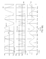
- Figs. 4 to 7 show the initial converter startup as the input voltage provided by VTEG 1 slowly increases from 0V.
- the top plot shows the input voltage provided at the VTEG 303.
- the middle plot depicts the voltage (see waveform 420) measured at the gate terminal of transistor M2 361 (GATE2) at the start point of the converter as well as the primary current (430) measured at L2 345.
- the bottom plot in Fig. 4 depicts the output voltage (440) measured at VOUT 380.
- Fig. 6 provides similar plots, where plot 510 corresponds to 410, plot 540 corresponds to 440, 530 corresponds to 420, with an exception that plot 520 corresponds to the voltage observed at the secondary winding at point SEC2 in Fig. 3 .
- Fig. 6 also provides plots related to the initial startup process, where plot 610 corresponds to 410, and plot 640 corresponds to plot 440.
- voltages observed at GATE1 and GATE 2 are plotted as 620 and 630 and it can be seen that when GATE2 in the bottom core circuit is active (see plot 620), GATE1 of the top core circuit is inactive (see plot 630).
- plot 7 provides another variation in depicting the initial startup process, in which plot 710 corresponds to plot 410 and plot 740 corresponds to plot 440, where the two plots in the middle represent the voltage observed at GATE2 (730) and the voltage observed at the drain terminal of transistor M2 361.
- Fig. 4 it can be seen that the negative polarity core circuit begins to self-oscillate at an input voltage of approximately 21mV.
- the depletion mode MOSFETs, M2 361 and M4 365 are conducting, due to the very low voltage across the gate to the source. This can be seen in the voltage waveform 420 plotted based on the observed voltage at the gate 2 terminal (see gates of MOSFETs M2 361 and M4 365 in Fig. 3 ). This is due to the depletion mode MOSFETs having a typical threshold voltage of approximately -0.5V, while the threshold voltage for standard MOSFETS is about 0.75V.
- MOSFET transistors M2 361 and M4 365 bridge the transformer primary, L2 345, across VTEG 1 with M4 365 providing the return path for VTEG1 and M2 361 driving one side of the primary winding and VTEG1 driving the opposite side of the primary winding.
- GATE2 The voltage on the gate terminal of M2 361 (GATE2) is phase shifted by 180 degrees at the drain of transistor M2 361 due to its common source amplifier configuration. This phase shifted voltage is applied across the primary of the transformer, L2 345, as described above. The transformer couples this signal to its secondary, L4 349.
- the secondary or magnetizing inductance of the transformer acts upon the effective secondary capacitance comprised of the MOSFET input capacitance and transformer winding capacitance, it imposes an additional 180 degree phase shift at the resonant frequency of the circuit.
- a positive feedback (360 degree phase shift) and a loop gain that is greater than unity are required. Both of these conditions are satisfied when the input voltage from VTEG1 is high enough to bring the depletion mode MOSFET M2 361 out of the linear region of operation, which is characterized by very low gain to its saturated region, characterized by high gain.
- the coupling capacitor, C10 351 connected on one side to SEC2 and on its other side to diode charge pump D1 373 and D4 375 transfers current to VOUT 380 via D4 375 when the oscillation polarity is positive and recharges C10 351 via D1 373 when the oscillation voltage polarity is negative.
- the steady state voltage across C10 351 is approximately equal to 1 ⁇ 2 the p-p amplitude of the oscillating waveform seen on the transformer secondary, SEC2.
- the oscillation amplitude observed at SEC2 is a function of the voltage applied to the transformer primary, which is, e.g., in an ideal situation VTEG 1 and the transformer turns ratio, 100:1 in the illustrated embodiment. It is understood that other transformer ratios can also be used.
- a lower turns ratio requires a higher startup voltage but will deliver greater power with a larger Vin applied, while the higher turns ratio will allow for lower startup voltages, but lower output power at higher input voltages.
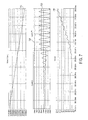
- Figs. 8-11 show waveforms observed at the gate terminal (GATE2) of transistor M2 361 and gate terminal (GATE1) of transistor M1 311 in circuit 300 when an instantaneous +/-100mV input voltage is applied.
- Zener clamps D3/D9 (367/371) and D2/D10 (327/329) limit the voltages at those gate terminals (GATE1 and GATE2) to approximately +/- 5V, which is required by the particular IC process employed. It is to be noted that when GATE2 is active, GATE 1 is not active and when the voltage polarity is switched, the opposite occurs. As the gate drive increases, the converter pulls more current from the input voltage source, VTEG1 303.
- Fig. 8 where when the VTEG switches from an input voltage of -100mV to +100mV (see plot 810), transistor M2 361 switches from active to inactive (see plot 820) and transistor M1 311 switches from inactive to active (see plot 830).
- the voltage measured at GATE2 is limited by the Zener diode clamp to about +/- 5V (820) and so is the voltage measured at GATE1 (830).
- the VOUT measured at 380 remains at its regulated value of 5V, regardless of the input voltage polarity applied to the converter. (see plot 840).
- Fig. 9 shows the input and output voltage relationship as well as voltages observed at different points within circuit 300.
- Waveform 910 represents the input voltage with a certain polarity.
- Waveform 950 represents the output voltage VOUT 380. As can be seen, the output voltage exhibits a small 1.4mV peak to peak ripple riding on the nominal 5V DC at the oscillation frequency of the converter.
- Waveform 920 represents the primary voltage of transformer L2
- waveform 930 represents the secondary voltage observed at SEC2
- waveform 940 represents the gate drive voltage observed at GATE2.
- Fig. 10 similarly shows the output voltage waveform 1070 as well as the voltage waveforms 1050 and 1060 based on voltages observed at GATE2 and SEC2, respectively.
- Waveform 1020 represents the current observed at the drain terminal of depletion mode device M4 365 displayed in comparison with the magnitude of the drain current in the standard threshold MOSFET t 1010 of transistor M7 363, once the circuit 300 is in regulation with a sufficient gate drive.
- Waveform 1040 represents the current observed at the drain terminal of the parallelly connected depletion mode device M2 361 displayed in comparison with the magnitude of drain current in the standard MOSFET threshold1030 of transistor M8 359 when the circuit 300 is in regulation with a sufficient gate drive.
- Fig. 11 in addition to the similar plots (output voltage 1170 and voltage waveforms 1150 and 1160 representing the voltages observed at GATE2 and SEC2) as those shown in Figs. 9 and 10 , the top two plots display the relative magnitude of the standard threshold MOSFETs for both halves of the converter when the output voltage is in regulation. Note how the drain currents of M8 359 and M6 339 (the non-active) side in this simulation are essentially zero.
- VTEG1 is modeled with a 1.5 ohm source resistance, as a result, the actual voltage applied across the primary is reduced and the resulting gate drive voltage is reduced proportionally to about +/-3.5V seen after the circuit has been in operation by - 20mS.
- non-zero source impedance devices such as Thermal Electric Generators (TEG)
- TEG Thermal Electric Generators
- TEG Thermal Electric Generators
Landscapes
- Engineering & Computer Science (AREA)
- Power Engineering (AREA)
- Dc-Dc Converters (AREA)
Applications Claiming Priority (3)
| Application Number | Priority Date | Filing Date | Title |
|---|---|---|---|
| US14421609P | 2009-01-13 | 2009-01-13 | |
| US25662809P | 2009-10-30 | 2009-10-30 | |
| EP10150693.9A EP2207258B1 (fr) | 2009-01-13 | 2010-01-13 | Convertisseur élévateur indépendant de la polarité capable de fonctionner dans des conditions de tension d'entrée ultra faible |
Related Parent Applications (2)
| Application Number | Title | Priority Date | Filing Date |
|---|---|---|---|
| EP10150693.9 Division | 2010-01-13 | ||
| EP10150693.9A Division EP2207258B1 (fr) | 2009-01-13 | 2010-01-13 | Convertisseur élévateur indépendant de la polarité capable de fonctionner dans des conditions de tension d'entrée ultra faible |
Publications (2)
| Publication Number | Publication Date |
|---|---|
| EP2575248A1 true EP2575248A1 (fr) | 2013-04-03 |
| EP2575248B1 EP2575248B1 (fr) | 2015-12-30 |
Family
ID=42154605
Family Applications (2)
| Application Number | Title | Priority Date | Filing Date |
|---|---|---|---|
| EP10150693.9A Active EP2207258B1 (fr) | 2009-01-13 | 2010-01-13 | Convertisseur élévateur indépendant de la polarité capable de fonctionner dans des conditions de tension d'entrée ultra faible |
| EP12008106.2A Active EP2575248B1 (fr) | 2009-01-13 | 2010-01-13 | Convertisseur élévateur indépendant de la polarité capable de fonctionner dans des conditions de tension d'entrée ultra faible |
Family Applications Before (1)
| Application Number | Title | Priority Date | Filing Date |
|---|---|---|---|
| EP10150693.9A Active EP2207258B1 (fr) | 2009-01-13 | 2010-01-13 | Convertisseur élévateur indépendant de la polarité capable de fonctionner dans des conditions de tension d'entrée ultra faible |
Country Status (3)
| Country | Link |
|---|---|
| US (1) | US9325250B2 (fr) |
| EP (2) | EP2207258B1 (fr) |
| TW (1) | TWI460980B (fr) |
Families Citing this family (14)
| Publication number | Priority date | Publication date | Assignee | Title |
|---|---|---|---|---|
| ITTO20110109A1 (it) * | 2011-02-09 | 2012-08-10 | Illinois Tool Works | Apparecchio di cottura con dispositivo di accensione alimentato da una termocoppia |
| DE102012221687B4 (de) * | 2012-11-28 | 2021-10-07 | Albert-Ludwigs-Universität Freiburg | Spannungswandler-Vollbrücke mit geringer Anlaufspannung |
| US9966838B2 (en) * | 2013-02-20 | 2018-05-08 | Texas Instruments Incorporated | Voltage conversion and charging from low bipolar input voltage |
| CN103107727B (zh) * | 2013-03-04 | 2015-11-18 | 杭州电子科技大学 | 用于微小能量采集的极低输入电压dc-ac转换电路 |
| CN104935169B (zh) * | 2014-03-17 | 2019-01-29 | 上海新物科技有限公司 | 直流电源升压电路 |
| US9866245B2 (en) * | 2015-11-18 | 2018-01-09 | Linear Technology Corporation | Active differential resistors with reduced noise |
| EP3255795A1 (fr) * | 2016-06-10 | 2017-12-13 | Goodrich Control Systems | Commutateur de puissance |
| CN109564441B (zh) * | 2016-06-14 | 2021-07-27 | 阿里埃勒科学创新有限公司 | 热电发电机 |
| DE202018000753U1 (de) * | 2018-02-14 | 2019-05-16 | Matrix Industries, Inc. | Startschaltung für Energy Harvesting Schaltungen |
| DE202018000752U1 (de) * | 2018-02-14 | 2019-05-16 | Matrix Industries, Inc. | Startschaltung für Energy Harvesting Schaltungen |
| US10778104B2 (en) * | 2018-09-14 | 2020-09-15 | National Research Council Of Canada | Efficient electricity conversion for harvesting energy from low voltage sources |
| WO2021253122A1 (fr) * | 2020-06-16 | 2021-12-23 | National Research Council Of Canada | Redressement synchrone pour améliortion de l'efficacité de conversion d'électricité pour collecter de l'énergie à partir de sources basse-tension |
| JP7566506B2 (ja) | 2020-06-26 | 2024-10-15 | 旭化成エレクトロニクス株式会社 | 電力供給装置 |
| US20240313663A1 (en) * | 2023-03-14 | 2024-09-19 | Ablic Inc. | Controller and self-oscillation dc-dc converter including the controller |
Citations (1)
| Publication number | Priority date | Publication date | Assignee | Title |
|---|---|---|---|---|
| US6340787B1 (en) * | 1996-12-02 | 2002-01-22 | Janick Simeray | Power converter for supplying electricity from a difference in temperature |
Family Cites Families (13)
| Publication number | Priority date | Publication date | Assignee | Title |
|---|---|---|---|---|
| US2214864A (en) * | 1938-08-16 | 1940-09-17 | Gen Electric | Variable transformer |
| US4559590A (en) * | 1983-03-24 | 1985-12-17 | Varian Associates, Inc. | Regulated DC to DC converter |
| US4890210A (en) * | 1988-11-15 | 1989-12-26 | Gilbarco, Inc. | Power supply having combined forward converter and flyback action for high efficiency conversion from low to high voltage |
| US5331258A (en) * | 1992-03-30 | 1994-07-19 | Solaria Research Enterprises, Ltd. | Synchronous-rectification type control for direct current motors and method of making |
| US6177829B1 (en) * | 1997-11-19 | 2001-01-23 | Texas Instruments Incorporated | Device for improving the switching efficiency of an integrated circuit charge pump |
| US6082115A (en) * | 1998-12-18 | 2000-07-04 | National Semiconductor Corporation | Temperature regulator circuit and precision voltage reference for integrated circuit |
| US7298123B2 (en) * | 2000-02-08 | 2007-11-20 | The Furukawa Electric Co., Ltd. | Apparatus and circuit for power supply, and apparatus for controlling large current load |
| EP1388208B1 (fr) * | 2001-03-28 | 2007-01-10 | Koninklijke Philips Electronics N.V. | Redresseurs synchrones |
| US6678175B1 (en) * | 2002-08-15 | 2004-01-13 | Galaxy Power, Inc. | Utilizing charge stored in a snubber capacitator in a switching circuit |
| US7317265B2 (en) * | 2003-03-05 | 2008-01-08 | Honeywell International Inc. | Method and apparatus for power management |
| US6982883B2 (en) * | 2004-03-22 | 2006-01-03 | Summer Steven E | Radiation tolerant electrical component with non-radiation hardened FET |
| US7746674B2 (en) * | 2007-02-22 | 2010-06-29 | Leader Electronics Inc. | Self-oscillating power converter |
| US8231240B1 (en) * | 2007-12-12 | 2012-07-31 | Txl Group, Inc. | Surface lighting devices having a thermoelectric power source |
-
2010
- 2010-01-13 EP EP10150693.9A patent/EP2207258B1/fr active Active
- 2010-01-13 EP EP12008106.2A patent/EP2575248B1/fr active Active
- 2010-01-13 US US12/686,749 patent/US9325250B2/en active Active
- 2010-01-13 TW TW099100848A patent/TWI460980B/zh active
Patent Citations (1)
| Publication number | Priority date | Publication date | Assignee | Title |
|---|---|---|---|---|
| US6340787B1 (en) * | 1996-12-02 | 2002-01-22 | Janick Simeray | Power converter for supplying electricity from a difference in temperature |
Non-Patent Citations (1)
| Title |
|---|
| DOUSEKI T ET AL: "A batteryless wireless system uses ambient heat with a reversible-power-source compatible CMOS/SOI DC-DC converter", SOLID-STATE CIRCUITS CONFERENCE, 2003. DIGEST OF TECHNICAL PAPERS. ISS CC. 2003 IEEE INTERNATIONAL SAN FRANCISCO, CA, USA 9-13 FEB. 2003, PISCATAWAY, NJ, USA,IEEE, US, 9 February 2003 (2003-02-09), pages 1 - 10, XP010661629, ISBN: 978-0-7803-7707-3 * |
Also Published As
| Publication number | Publication date |
|---|---|
| TWI460980B (zh) | 2014-11-11 |
| EP2207258A2 (fr) | 2010-07-14 |
| US20100195360A1 (en) | 2010-08-05 |
| EP2207258A3 (fr) | 2012-03-14 |
| US9325250B2 (en) | 2016-04-26 |
| TW201031097A (en) | 2010-08-16 |
| EP2207258B1 (fr) | 2013-09-18 |
| EP2575248B1 (fr) | 2015-12-30 |
Similar Documents
| Publication | Publication Date | Title |
|---|---|---|
| EP2207258B1 (fr) | Convertisseur élévateur indépendant de la polarité capable de fonctionner dans des conditions de tension d'entrée ultra faible | |
| TWI354443B (en) | Half-bridge llc resonant converter with self-drive | |
| CN102246405B (zh) | 用于单相和多相系统的通用ac-dc同步整流技术 | |
| CN107086793B (zh) | 一种用于同步整流功率变换器的动态补偿控制电路 | |
| US8400789B2 (en) | Power supply with input filter-controlled switch clamp circuit | |
| US20100208498A1 (en) | Ultra-low voltage boost circuit | |
| US9054585B2 (en) | Low drop diode equivalent circuit | |
| CN110022068A (zh) | 具有有源钳位器的同步整流栅极驱动器 | |
| Desai et al. | A bipolar±40 mV self-starting boost converter with transformer reuse for thermoelectric energy harvesting | |
| CN104242612A (zh) | 用于驱动晶体管的方法和系统 | |
| Karthikeyan et al. | Signal-powered low-drop-diode equivalent circuit for full-wave bridge rectifier | |
| CN103262389A (zh) | 电力接收装置及使用其的非接触式电力传送系统 | |
| US9240753B2 (en) | Oscillator and power management apparatus | |
| US20210028718A1 (en) | Rectifier circuit | |
| CN109274258A (zh) | 具有起动电路的热电发电机 | |
| CN206962707U (zh) | 一种用于同步整流功率变换器的动态补偿控制电路 | |
| CN101557170B (zh) | 具自驱式同步整流器的半桥llc谐振转换器 | |
| Wardlaw et al. | Self-powered rectifier for energy harvesting applications | |
| US11342854B1 (en) | Voltage step-up converter circuits for low input voltages | |
| US8116107B2 (en) | Synchronous rectification control circuit assembly | |
| TWM340660U (en) | Half-bridge llc resonant conver with self-driven synchronous rectifier | |
| Xu et al. | A new class of integrated CMOS rectifiers with improved PVT-compensated efficiency | |
| Gao et al. | A 60 mV-3 V input range boost converter with amplitude-regulated and intermittently operating oscillator for energy harvesting | |
| AU2016100186A4 (en) | Converter circuit and operating method thereof | |
| US12597855B2 (en) | Power supply device with high output stability |
Legal Events
| Date | Code | Title | Description |
|---|---|---|---|
| PUAI | Public reference made under article 153(3) epc to a published international application that has entered the european phase |
Free format text: ORIGINAL CODE: 0009012 |
|
| AC | Divisional application: reference to earlier application |
Ref document number: 2207258 Country of ref document: EP Kind code of ref document: P |
|
| AK | Designated contracting states |
Kind code of ref document: A1 Designated state(s): AT BE BG CH CY CZ DE DK EE ES FI FR GB GR HR HU IE IS IT LI LT LU LV MC MK MT NL NO PL PT RO SE SI SK SM TR |
|
| 17P | Request for examination filed |
Effective date: 20131002 |
|
| RBV | Designated contracting states (corrected) |
Designated state(s): AT BE BG CH CY CZ DE DK EE ES FI FR GB GR HR HU IE IS IT LI LT LU LV MC MK MT NL NO PL PT RO SE SI SK SM TR |
|
| GRAP | Despatch of communication of intention to grant a patent |
Free format text: ORIGINAL CODE: EPIDOSNIGR1 |
|
| INTG | Intention to grant announced |
Effective date: 20150413 |
|
| GRAR | Information related to intention to grant a patent recorded |
Free format text: ORIGINAL CODE: EPIDOSNIGR71 |
|
| GRAS | Grant fee paid |
Free format text: ORIGINAL CODE: EPIDOSNIGR3 |
|
| GRAA | (expected) grant |
Free format text: ORIGINAL CODE: 0009210 |
|
| INTG | Intention to grant announced |
Effective date: 20151102 |
|
| AC | Divisional application: reference to earlier application |
Ref document number: 2207258 Country of ref document: EP Kind code of ref document: P |
|
| AK | Designated contracting states |
Kind code of ref document: B1 Designated state(s): AT BE BG CH CY CZ DE DK EE ES FI FR GB GR HR HU IE IS IT LI LT LU LV MC MK MT NL NO PL PT RO SE SI SK SM TR |
|
| REG | Reference to a national code |
Ref country code: GB Ref legal event code: FG4D |
|
| REG | Reference to a national code |
Ref country code: CH Ref legal event code: EP |
|
| REG | Reference to a national code |
Ref country code: AT Ref legal event code: REF Ref document number: 767870 Country of ref document: AT Kind code of ref document: T Effective date: 20160115 |
|
| REG | Reference to a national code |
Ref country code: FR Ref legal event code: PLFP Year of fee payment: 7 |
|
| REG | Reference to a national code |
Ref country code: IE Ref legal event code: FG4D |
|
| REG | Reference to a national code |
Ref country code: DE Ref legal event code: R096 Ref document number: 602010029802 Country of ref document: DE |
|
| REG | Reference to a national code |
Ref country code: NL Ref legal event code: FP |
|
| REG | Reference to a national code |
Ref country code: LT Ref legal event code: MG4D |
|
| PG25 | Lapsed in a contracting state [announced via postgrant information from national office to epo] |
Ref country code: HR Free format text: LAPSE BECAUSE OF FAILURE TO SUBMIT A TRANSLATION OF THE DESCRIPTION OR TO PAY THE FEE WITHIN THE PRESCRIBED TIME-LIMIT Effective date: 20151230 Ref country code: NO Free format text: LAPSE BECAUSE OF FAILURE TO SUBMIT A TRANSLATION OF THE DESCRIPTION OR TO PAY THE FEE WITHIN THE PRESCRIBED TIME-LIMIT Effective date: 20160330 Ref country code: LT Free format text: LAPSE BECAUSE OF FAILURE TO SUBMIT A TRANSLATION OF THE DESCRIPTION OR TO PAY THE FEE WITHIN THE PRESCRIBED TIME-LIMIT Effective date: 20151230 |
|
| REG | Reference to a national code |
Ref country code: AT Ref legal event code: MK05 Ref document number: 767870 Country of ref document: AT Kind code of ref document: T Effective date: 20151230 |
|
| PG25 | Lapsed in a contracting state [announced via postgrant information from national office to epo] |
Ref country code: LV Free format text: LAPSE BECAUSE OF FAILURE TO SUBMIT A TRANSLATION OF THE DESCRIPTION OR TO PAY THE FEE WITHIN THE PRESCRIBED TIME-LIMIT Effective date: 20151230 Ref country code: BE Free format text: LAPSE BECAUSE OF NON-PAYMENT OF DUE FEES Effective date: 20160131 Ref country code: SE Free format text: LAPSE BECAUSE OF FAILURE TO SUBMIT A TRANSLATION OF THE DESCRIPTION OR TO PAY THE FEE WITHIN THE PRESCRIBED TIME-LIMIT Effective date: 20151230 Ref country code: GR Free format text: LAPSE BECAUSE OF FAILURE TO SUBMIT A TRANSLATION OF THE DESCRIPTION OR TO PAY THE FEE WITHIN THE PRESCRIBED TIME-LIMIT Effective date: 20160331 Ref country code: FI Free format text: LAPSE BECAUSE OF FAILURE TO SUBMIT A TRANSLATION OF THE DESCRIPTION OR TO PAY THE FEE WITHIN THE PRESCRIBED TIME-LIMIT Effective date: 20151230 |
|
| PG25 | Lapsed in a contracting state [announced via postgrant information from national office to epo] |
Ref country code: ES Free format text: LAPSE BECAUSE OF FAILURE TO SUBMIT A TRANSLATION OF THE DESCRIPTION OR TO PAY THE FEE WITHIN THE PRESCRIBED TIME-LIMIT Effective date: 20151230 Ref country code: CZ Free format text: LAPSE BECAUSE OF FAILURE TO SUBMIT A TRANSLATION OF THE DESCRIPTION OR TO PAY THE FEE WITHIN THE PRESCRIBED TIME-LIMIT Effective date: 20151230 |
|
| PG25 | Lapsed in a contracting state [announced via postgrant information from national office to epo] |
Ref country code: RO Free format text: LAPSE BECAUSE OF FAILURE TO SUBMIT A TRANSLATION OF THE DESCRIPTION OR TO PAY THE FEE WITHIN THE PRESCRIBED TIME-LIMIT Effective date: 20151230 Ref country code: EE Free format text: LAPSE BECAUSE OF FAILURE TO SUBMIT A TRANSLATION OF THE DESCRIPTION OR TO PAY THE FEE WITHIN THE PRESCRIBED TIME-LIMIT Effective date: 20151230 Ref country code: SM Free format text: LAPSE BECAUSE OF FAILURE TO SUBMIT A TRANSLATION OF THE DESCRIPTION OR TO PAY THE FEE WITHIN THE PRESCRIBED TIME-LIMIT Effective date: 20151230 Ref country code: LU Free format text: LAPSE BECAUSE OF FAILURE TO SUBMIT A TRANSLATION OF THE DESCRIPTION OR TO PAY THE FEE WITHIN THE PRESCRIBED TIME-LIMIT Effective date: 20160113 Ref country code: SK Free format text: LAPSE BECAUSE OF FAILURE TO SUBMIT A TRANSLATION OF THE DESCRIPTION OR TO PAY THE FEE WITHIN THE PRESCRIBED TIME-LIMIT Effective date: 20151230 Ref country code: PT Free format text: LAPSE BECAUSE OF FAILURE TO SUBMIT A TRANSLATION OF THE DESCRIPTION OR TO PAY THE FEE WITHIN THE PRESCRIBED TIME-LIMIT Effective date: 20160502 Ref country code: PL Free format text: LAPSE BECAUSE OF FAILURE TO SUBMIT A TRANSLATION OF THE DESCRIPTION OR TO PAY THE FEE WITHIN THE PRESCRIBED TIME-LIMIT Effective date: 20151230 Ref country code: IS Free format text: LAPSE BECAUSE OF FAILURE TO SUBMIT A TRANSLATION OF THE DESCRIPTION OR TO PAY THE FEE WITHIN THE PRESCRIBED TIME-LIMIT Effective date: 20160430 Ref country code: AT Free format text: LAPSE BECAUSE OF FAILURE TO SUBMIT A TRANSLATION OF THE DESCRIPTION OR TO PAY THE FEE WITHIN THE PRESCRIBED TIME-LIMIT Effective date: 20151230 |
|
| REG | Reference to a national code |
Ref country code: CH Ref legal event code: PL |
|
| PG25 | Lapsed in a contracting state [announced via postgrant information from national office to epo] |
Ref country code: MC Free format text: LAPSE BECAUSE OF FAILURE TO SUBMIT A TRANSLATION OF THE DESCRIPTION OR TO PAY THE FEE WITHIN THE PRESCRIBED TIME-LIMIT Effective date: 20151230 |
|
| REG | Reference to a national code |
Ref country code: DE Ref legal event code: R097 Ref document number: 602010029802 Country of ref document: DE |
|
| PG25 | Lapsed in a contracting state [announced via postgrant information from national office to epo] |
Ref country code: DK Free format text: LAPSE BECAUSE OF FAILURE TO SUBMIT A TRANSLATION OF THE DESCRIPTION OR TO PAY THE FEE WITHIN THE PRESCRIBED TIME-LIMIT Effective date: 20151230 Ref country code: CH Free format text: LAPSE BECAUSE OF NON-PAYMENT OF DUE FEES Effective date: 20160131 Ref country code: LI Free format text: LAPSE BECAUSE OF NON-PAYMENT OF DUE FEES Effective date: 20160131 |
|
| REG | Reference to a national code |
Ref country code: IE Ref legal event code: MM4A |
|
| PLBE | No opposition filed within time limit |
Free format text: ORIGINAL CODE: 0009261 |
|
| STAA | Information on the status of an ep patent application or granted ep patent |
Free format text: STATUS: NO OPPOSITION FILED WITHIN TIME LIMIT |
|
| 26N | No opposition filed |
Effective date: 20161003 |
|
| PG25 | Lapsed in a contracting state [announced via postgrant information from national office to epo] |
Ref country code: BE Free format text: LAPSE BECAUSE OF FAILURE TO SUBMIT A TRANSLATION OF THE DESCRIPTION OR TO PAY THE FEE WITHIN THE PRESCRIBED TIME-LIMIT Effective date: 20151230 |
|
| REG | Reference to a national code |
Ref country code: FR Ref legal event code: PLFP Year of fee payment: 8 |
|
| PG25 | Lapsed in a contracting state [announced via postgrant information from national office to epo] |
Ref country code: IE Free format text: LAPSE BECAUSE OF NON-PAYMENT OF DUE FEES Effective date: 20160113 |
|
| PG25 | Lapsed in a contracting state [announced via postgrant information from national office to epo] |
Ref country code: SI Free format text: LAPSE BECAUSE OF FAILURE TO SUBMIT A TRANSLATION OF THE DESCRIPTION OR TO PAY THE FEE WITHIN THE PRESCRIBED TIME-LIMIT Effective date: 20151230 |
|
| PG25 | Lapsed in a contracting state [announced via postgrant information from national office to epo] |
Ref country code: MT Free format text: LAPSE BECAUSE OF FAILURE TO SUBMIT A TRANSLATION OF THE DESCRIPTION OR TO PAY THE FEE WITHIN THE PRESCRIBED TIME-LIMIT Effective date: 20151230 |
|
| REG | Reference to a national code |
Ref country code: FR Ref legal event code: PLFP Year of fee payment: 9 |
|
| PG25 | Lapsed in a contracting state [announced via postgrant information from national office to epo] |
Ref country code: HU Free format text: LAPSE BECAUSE OF FAILURE TO SUBMIT A TRANSLATION OF THE DESCRIPTION OR TO PAY THE FEE WITHIN THE PRESCRIBED TIME-LIMIT; INVALID AB INITIO Effective date: 20100113 Ref country code: CY Free format text: LAPSE BECAUSE OF FAILURE TO SUBMIT A TRANSLATION OF THE DESCRIPTION OR TO PAY THE FEE WITHIN THE PRESCRIBED TIME-LIMIT Effective date: 20151230 |
|
| PG25 | Lapsed in a contracting state [announced via postgrant information from national office to epo] |
Ref country code: MK Free format text: LAPSE BECAUSE OF FAILURE TO SUBMIT A TRANSLATION OF THE DESCRIPTION OR TO PAY THE FEE WITHIN THE PRESCRIBED TIME-LIMIT Effective date: 20151230 Ref country code: TR Free format text: LAPSE BECAUSE OF FAILURE TO SUBMIT A TRANSLATION OF THE DESCRIPTION OR TO PAY THE FEE WITHIN THE PRESCRIBED TIME-LIMIT Effective date: 20151230 Ref country code: MT Free format text: LAPSE BECAUSE OF FAILURE TO SUBMIT A TRANSLATION OF THE DESCRIPTION OR TO PAY THE FEE WITHIN THE PRESCRIBED TIME-LIMIT Effective date: 20160131 |
|
| PG25 | Lapsed in a contracting state [announced via postgrant information from national office to epo] |
Ref country code: BG Free format text: LAPSE BECAUSE OF FAILURE TO SUBMIT A TRANSLATION OF THE DESCRIPTION OR TO PAY THE FEE WITHIN THE PRESCRIBED TIME-LIMIT Effective date: 20151230 |
|
| REG | Reference to a national code |
Ref country code: DE Ref legal event code: R082 Ref document number: 602010029802 Country of ref document: DE Representative=s name: MUELLER-BORE & PARTNER PATENTANWAELTE PARTG MB, DE Ref country code: DE Ref legal event code: R081 Ref document number: 602010029802 Country of ref document: DE Owner name: ANALOG DEVICES INTERNATIONAL UNLIMITED COMPANY, IE Free format text: FORMER OWNER: LINEAR TECHNOLOGY CORPORATION, MILPITAS, CALIF., US Ref country code: DE Ref legal event code: R082 Ref document number: 602010029802 Country of ref document: DE Representative=s name: WITHERS & ROGERS LLP, DE |
|
| REG | Reference to a national code |
Ref country code: DE Ref legal event code: R082 Ref document number: 602010029802 Country of ref document: DE Representative=s name: WITHERS & ROGERS LLP, DE |
|
| REG | Reference to a national code |
Ref country code: GB Ref legal event code: 732E Free format text: REGISTERED BETWEEN 20211202 AND 20211209 |
|
| REG | Reference to a national code |
Ref country code: NL Ref legal event code: PD Owner name: ANALOG DEVICES INTERNATIONAL UNLIMITED COMPANY; IE Free format text: DETAILS ASSIGNMENT: CHANGE OF OWNER(S), ASSIGNMENT; FORMER OWNER NAME: LINEAR TECHNOLOGY LLC Effective date: 20211216 |
|
| PGFP | Annual fee paid to national office [announced via postgrant information from national office to epo] |
Ref country code: IT Payment date: 20220103 Year of fee payment: 13 |
|
| PGFP | Annual fee paid to national office [announced via postgrant information from national office to epo] |
Ref country code: GB Payment date: 20231219 Year of fee payment: 15 |
|
| PG25 | Lapsed in a contracting state [announced via postgrant information from national office to epo] |
Ref country code: IT Free format text: LAPSE BECAUSE OF NON-PAYMENT OF DUE FEES Effective date: 20230113 |
|
| PGFP | Annual fee paid to national office [announced via postgrant information from national office to epo] |
Ref country code: NL Payment date: 20231219 Year of fee payment: 15 Ref country code: FR Payment date: 20231219 Year of fee payment: 15 |
|
| PGFP | Annual fee paid to national office [announced via postgrant information from national office to epo] |
Ref country code: DE Payment date: 20241218 Year of fee payment: 16 |
|
| REG | Reference to a national code |
Ref country code: NL Ref legal event code: MM Effective date: 20250201 |
|
| GBPC | Gb: european patent ceased through non-payment of renewal fee |
Effective date: 20250113 |
|
| PG25 | Lapsed in a contracting state [announced via postgrant information from national office to epo] |
Ref country code: NL Free format text: LAPSE BECAUSE OF NON-PAYMENT OF DUE FEES Effective date: 20250201 |
|
| PG25 | Lapsed in a contracting state [announced via postgrant information from national office to epo] |
Ref country code: GB Free format text: LAPSE BECAUSE OF NON-PAYMENT OF DUE FEES Effective date: 20250113 |
|
| PG25 | Lapsed in a contracting state [announced via postgrant information from national office to epo] |
Ref country code: FR Free format text: LAPSE BECAUSE OF NON-PAYMENT OF DUE FEES Effective date: 20250131 |