EP2575253A1 - Branch ciruit - Google Patents
Branch ciruit Download PDFInfo
- Publication number
- EP2575253A1 EP2575253A1 EP12162033A EP12162033A EP2575253A1 EP 2575253 A1 EP2575253 A1 EP 2575253A1 EP 12162033 A EP12162033 A EP 12162033A EP 12162033 A EP12162033 A EP 12162033A EP 2575253 A1 EP2575253 A1 EP 2575253A1
- Authority
- EP
- European Patent Office
- Prior art keywords
- band
- pass filter
- coil
- capacitor
- signal
- Prior art date
- Legal status (The legal status is an assumption and is not a legal conclusion. Google has not performed a legal analysis and makes no representation as to the accuracy of the status listed.)
- Withdrawn
Links
Images




Classifications
-
- H—ELECTRICITY
- H03—ELECTRONIC CIRCUITRY
- H03H—IMPEDANCE NETWORKS, e.g. RESONANT CIRCUITS; RESONATORS
- H03H7/00—Multiple-port networks comprising only passive electrical elements as network components
- H03H7/46—Networks for connecting several sources or loads, working on different frequencies or frequency bands, to a common load or source
- H03H7/463—Duplexers
-
- H—ELECTRICITY
- H03—ELECTRONIC CIRCUITRY
- H03H—IMPEDANCE NETWORKS, e.g. RESONANT CIRCUITS; RESONATORS
- H03H7/00—Multiple-port networks comprising only passive electrical elements as network components
- H03H7/01—Frequency selective two-port networks
- H03H7/0115—Frequency selective two-port networks comprising only inductors and capacitors
-
- H—ELECTRICITY
- H03—ELECTRONIC CIRCUITRY
- H03H—IMPEDANCE NETWORKS, e.g. RESONANT CIRCUITS; RESONATORS
- H03H7/00—Multiple-port networks comprising only passive electrical elements as network components
- H03H7/01—Frequency selective two-port networks
- H03H7/17—Structural details of sub-circuits of frequency selective networks
- H03H7/1741—Comprising typical LC combinations, irrespective of presence and location of additional resistors
- H03H7/175—Series LC in series path
-
- H—ELECTRICITY
- H03—ELECTRONIC CIRCUITRY
- H03H—IMPEDANCE NETWORKS, e.g. RESONANT CIRCUITS; RESONATORS
- H03H7/00—Multiple-port networks comprising only passive electrical elements as network components
- H03H7/01—Frequency selective two-port networks
- H03H7/17—Structural details of sub-circuits of frequency selective networks
- H03H7/1741—Comprising typical LC combinations, irrespective of presence and location of additional resistors
- H03H7/1758—Series LC in shunt or branch path
-
- H—ELECTRICITY
- H03—ELECTRONIC CIRCUITRY
- H03H—IMPEDANCE NETWORKS, e.g. RESONANT CIRCUITS; RESONATORS
- H03H7/00—Multiple-port networks comprising only passive electrical elements as network components
- H03H7/01—Frequency selective two-port networks
- H03H7/17—Structural details of sub-circuits of frequency selective networks
- H03H7/1741—Comprising typical LC combinations, irrespective of presence and location of additional resistors
- H03H7/1775—Parallel LC in shunt or branch path
Definitions
- the present invention relates to a branch circuit, and more particularly to the branch circuit for separating a first band signal, and a second band signal different from the first band signal from an input signal.
- Branch circuits are circuits that separate signals in a plurality of frequency bands from an input signal. Use of the branch circuits enables a signal in a frequency band (174 to 240 MHz) of DAB (Digital Audio Broadcast) and a signal in a frequency band (76 to 108 MHz) of FM (Frequency Modulation) broadcasting to be separated from an input signal.
- the branch circuits have a band-pass filter for allowing signals in the frequency band of DAB to pass through, and a band-pass filter for allowing the signals in the frequency band of FM broadcasting to pass through.
- the band-pass filters are circuits for allowing signals in a desired band to pass through and attenuating signals other than ones in the desired band.
- band-pass filters using an operational amplifier are known.
- resonator-coupling type band-pass filters using a parallel resonance circuit having a coil and a capacitor connected to the coil in parallel are known.
- JP Patent publication 11-298202 describes a resonator-coupling type band-pass filter having two parallel resonance circuits. The band-pass filter in the Patent Document is formed so that the two parallel resonance circuits are connected to each other into n type.
- One of characteristics of the resonator-coupling type band-pass filters is a steep frequency characteristic. Use of the resonator-coupling type band-pass filter enables a narrow-band signal to be separated from an input signal.
- an input impedance in a pass band is higher than an input impedance in bands other than the pass band.
- the parallel resonance circuits are grounded, signals other than the pass band signal pass through the parallel resonance circuits so as to output to the ground. Therefore, when a first band signal and a second band signal are separated from an input signal, the use of the resonator-coupling type band-pass filters for passing of the first band signal causes an increase in loss of the second band signal.
- a branch circuit of the present invention for separating a first band signal and a second band signal different from the first band signal from an input signal comprises: a first band-pass filter for allowing the first band signal in the input signal to pass through; and a second band-pass filter for allowing the second band signal in the input signal to pass through.
- the first band-pass filter includes; a pre-resonance circuit having a first coil and a first capacitor connected to the first coil in series, the pre-resonance circuit being connected to an input terminal of the first band-pass filter, a post-resonance circuit having a second coil and a second capacitor connected to the second coil in series, and the post-resonance circuit being connected between the pre-resonance circuit and an output terminal of the first band-pass filter, and a third coil connected between the output terminal of the pre-resonance circuit and a ground.
- an input impedance of a first band-pass filter in a first band becomes lower than an input impedance in bands other than the first band. Since the second band signal is prevented from being output to the ground via the first band-pass filter, the loss of the second band signal can be prevented.
- the first band-pass filter further includes a third capacitor connected between the third coil and the ground.
- a cutoff characteristic of the first band-pass filter in the first band can be made to be steep.
- an impedance of the first band-pass filter is represented by Z L
- a center frequency of the first band-pass filter is represented by f 0
- a bandwidth of the first band-pass filter is represented by ⁇ f
- constants are represented by g1 and g2
- an inductance L s1 of the first coil and an inductance L s2 of the second coil is expressed by the following (Formula 1)
- a capacitance C s1 of the first capacitor and a capacitance C s2 of the second capacitor are expressed by (Formula 2)
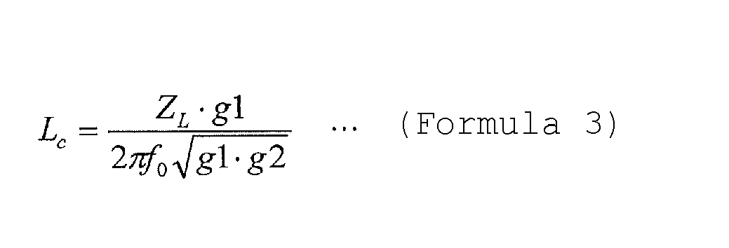
- the inductance L c of the third coil is expressed by (Formula 3).
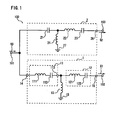
- Fig. 1 is a circuit diagram illustrating a branch circuit 100 according to the embodiment.
- the branch circuit 100 is provided with band-pass filters 1 and 2, an input terminal 101, output terminals 102 and 103.
- the band-pass filter 1 is connected between the input terminal 101 and the output terminal 102.
- the band-pass filter 2 is connected between the input terminal 101 and the output terminal 103.
- the branch circuit 100 inputs an input signal 50 from the input terminal 101.
- the band-pass filter 1 allows a first band signal 51 in the input signal 50 to pass through.
- the first band signal 51 that passes through the band-pass filter 1 is output from the output terminal 102.
- the band-pass filter 2 allows a second band signal 52 in the input signal 50 to pass through.
- the second band signal 52 that passes through the band-pass filter 2 is output from the output terminal 103.
- the first band is a frequency band (174 to 240 MHz) of DAB.
- the second band is a frequency band (76 to 108 MHz) of FM broadcasting.
- the first band and the second band are not limited to these frequency bands.
- the second band may be a frequency band higher than the first band or lower than the first band.
- the band-pass filter 1 is a resonator-coupling type band-pass filter.
- the band-pass filter 1 has a pre-resonance circuit 11, a post-resonance circuit 12, a coil 13, an input terminal 14, and an output terminal 15.
- the pre-resonance circuit 11 is a series resonance circuit that has a coil 111, and a capacitor 112 connected to the coil 111 in series.
- the pre-resonance circuit 11 is connected to the input terminal 14.
- the pre-resonance circuit 11 further has the output terminal 113.
- One end of the coil 111 is connected to the input terminal 14, and the other end of the coil 111 is connected to the capacitor 112.
- the capacitor 112 is connected between the coil 111 and the output terminal 113.
- the post-resonance circuit 12 is a series resonance circuit that has a coil 121, and a capacitor 122 connected to the coil 121 in series.
- the post-resonance circuit 12 is connected between the output terminal 15 of the pre-resonance circuit 11 and the output terminal 113 of the band-pass filter 1.
- One end of the coil 121 is connected to the output terminal 113, and the other end is connected to the capacitor 122.
- the capacitor 122 is connected between the coil 121 and the output terminal 15.
- the coil 13 is connected between the output terminal 113 and a ground 15.
- the band-pass filter 2 has capacitors 21 and 23, coils 22 and 24, and an output terminal 26.
- One end of the capacitor 21 is connected to the input terminal 101, and the other end of the capacitor 21 is connected to one end of the coil 22.
- the other end of the coil 22 is connected to one end of the capacitors 23.
- the other end of the capacitors 23 is connected to the output terminal 26.
- the coil 24 is connected between the other end of the capacitor 21 and a ground 27.
- the constitution of the band-pass filter 2 is not limited to the above constitution.
- the band-pass filter 1 is a resonator-coupling type band-pass filter that has two series resonance circuits (the pre-resonance circuit 11 and the post-resonance circuit 12).
- the band-pass filter 1 an input impedance in frequency bands other than the first band is higher than an input impedance in the first band.
- the branch circuit 100 can prevent loss of the second band signal 52 and can separate the first band signal 51 and the second band signal 52 from the input signal 50.
- a resonance frequency of the pre-resonance circuit 11 matches with a resonance frequency of the post-resonance circuit 12. As a result, a frequency characteristic of a steep gain can be obtained.
- an inductance of the coil 111 matches with an inductance of the coil 121.
- a capacitance of the capacitor 112 matches with a capacitance of the capacitor 122.
- a center frequency of the resonance circuit composed of the pre-resonance circuit 11 and the coil 13 deviates from a center frequency of the resonance circuit composed of the post-resonance circuit 12 and the coil 13.
- a bandwidth of the band-pass filter 1 is widened, the frequency characteristic of a steep gain cannot be obtained.
- Fig. 2 is a circuit diagram illustrating a normalization low-pass filter 60.
- the normalization low-pass filter 60 has a coil 61, a capacitor 62, an input terminal 63, and an output terminal 64.
- One end of the coil 61 is connected to the input terminal 63, and the other end of the coil 61 is connected to the output terminal 64.
- the capacitor 62 is connected between the other end of the coil 61 and a ground 65.
- an impedance is 1 ⁇ .
- a cutoff frequency is (1/2 ⁇ ) Hz. Therefore, an inductance of the coil 61 is 1.41421 H.
- a capacitance of the capacitor 62 is 1.41421 F.
- the center frequency, the bandwidth, and the impedance of the band-pass filter 1 are represented by f 0 , ⁇ f, and Z L .
- the values of the coils 13, 111 and 121, and the values of the capacitors 112 and 114 are calculated by using these parameters.
- K 12 is defined by using the normalization coupling constant k 12 according to the following (Formula 6).
- K 12 ⁇ ⁇ f f 0 ⁇ g ⁇ 1 ⁇ g ⁇ 2
- the constant K 12 is a numerical value such that the normalization coupling constant k 12 is changed according to the center frequency f 0 and the bandwidth ⁇ f.
- the constant K 12 is a characteristic value of a coupled circuit where the pre-resonance circuit 11 is coupled with the post-resonance circuit 12. In this embodiment, the coupled circuit corresponds to the coil 13.
- Provisional values (hereinafter, called provisional capacitances) of capacitances of the capacitors 112 and 122 are represented by C t1 .
- the provisional capacitances C t1 may be any values.
- Provisional values of the inductances of the coils 111 and 121 (hereinafter, "provisional inductance") L t1 are calculated by using the following (Formula 7).
- the provisional inductances L t1 are calculated as the inductances of the coils resonating with the provisional capacitances C t1 .
- L t ⁇ 1 1 2 ⁇ ⁇ ⁇ f 0 2 ⁇ C t ⁇ 1
- a provisional value of the inductance of the coupled circuit (the coil 13) (hereinafter, “provisional coupled inductance”) L ct is calculated according to the following (Formula 8).
- L ct K 12 ⁇
- L t ⁇ 1 ⁇ ⁇ f 2 ⁇ ⁇ ⁇ f 0 3 ⁇ C t ⁇ 1 ⁇ g ⁇ 1 ⁇ g ⁇ 2
- the inductance L ct of the coil 13 is subtracted from the provisional inductance L t1 of the coils 111 and 121.
- the coupled circuit (the coil 13) as well as the coil 111 resonates with the capacitor 112. Further, the coupled circuit (the coil 13) as well as the coil 121 resonates with the capacitor 122. For this reason, when the coils 111 and 121 of the provisional inductances L t1 are used directly, the center frequency of the band-pass filter 1 deviates from f 0 .
- the provisional inductances L t1 are adjusted by using the following (Formula 9) so that the deviation does not occur.
- the provisional capacitances C t1 , the provisional inductances L t2 , and the provisional coupled inductances L ct are changed according to the input impedance R L of the band-pass filter 1.
- An input impedance Z1 and an output impedance Z2 of the band-pass filter 1 are calculated by using the following (Formula 10) and (Formula 11).
- Z ⁇ 1 ⁇ ⁇ f 2 ⁇ ⁇ ⁇ f 0 2 ⁇ C t ⁇ 1 ⁇ g ⁇ 1
- Z ⁇ 2 ⁇ ⁇ f 2 ⁇ ⁇ ⁇ f 0 2 ⁇ C t ⁇ 1 ⁇ g ⁇ 2
- the input impedance Z1 and the output impedance Z2 have the same value. Further, since the input impedance Z1 and the output impedance Z2 include the provisional capacitance C t1 , they correspond to a provisional value of the impedance of the band-pass filter 1.
- a ratio R between the impedance R L of the band-pass filter 1 and the impedance Z1 is calculated by using the following (Formula 12).
- the provisional capacitance C t1 is multiplied by an inverse of the ratio R, so that a capacitance C s1 of the capacitor 112 and a capacitance C s2 of the capacitor 122 are obtained.
- the coupled circuit is composed of the coil 13. Therefore, an inductance L c of the coil 13 is calculated by multiplying the provisional coupled inductance L ct by the ratio R as expressed in the following (Formula 15).
- g1 and g2 are constants. Therefore, it is found that the inductances L c , L s1 and L s2 of the coils 13, 111 and 121, and the capacitances C s1 and C s2 of the capacitors 112 and 122 are determined by the impedance R L , the center frequency f 0 and the bandwidth ⁇ f of the band-pass filter 1.
- the frequency characteristic of the band-pass filter 1 will be described below. Parameters of the band-pass filter 1 were set, and the frequency characteristic of the band-pass filter 1 was simulated.
- the center frequency f 0 , the bandwidth ⁇ f and the impedance Z L of the band-pass filter 1 were set to 207 MHz, 105 MHz and 75 ⁇ .
- the inductances L s1 and L s2 of the coils 111 and 121 were set to 103.1 nH, and the capacitances C s1 and C s2 of the capacitors 112 and 122 were set to 3.667 pF.
- the inductance L c of the coil 13 was set to 57.66 nH.
- Fig. 3 is a Bode diagram illustrating a simulated result of the frequency characteristic (cutoff characteristic) of the gain in the band-pass filter 1.
- Fig. 4 is a graph illustrating a simulation result of the frequency characteristic of the input impedance in the band-pass filter 1.
- the gain of the band-pass filter 1 has a peak in the first band (174 to 240 MHz).
- the input impedance of the band-pass filter 1 reduces from the center frequency f 0 (207 MHz). That is to say, the input impedance in the first band is lower than the input impedances in bands other than the first band.
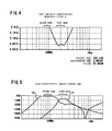
- FIG. 5 is a Bode diagram illustrating a simulated result of the frequency characteristic (cutoff characteristic) of the gain of the branch circuit 100.
- Fig. 6 is a graph illustrating a simulated result of a frequency characteristic of the input impedance of the branch circuit 100.
- the values of the respective elements of the band-pass filter 1 are the same as the values set at the time of the simulation of the band-pass filter 1.
- the capacitance of the capacitor 21 was set to 18 pF
- the capacitance of the capacitors 23 was set to 5.6 pF.
- a reactance of the coil 22 was set to 560 mH
- a reactance of the coil 24 was set to 270 mH.
- a curved line 71 corresponds to the frequency characteristic of the gain of the band-pass filter 1
- a curved line 72 corresponds to the frequency characteristic of the gain of the band-pass filter 2. Since the peak is present in the first band and the second band, it is found that the branch circuit 100 can separate the first band signal 51 and the second band signal 52 from the input signal 50.
- a curved line 81 corresponds to the frequency characteristic of the input impedance of the band-pass filter 1.
- a curved line 82 corresponds to the frequency characteristic of the input impedance of the band-pass filter 2.
- the input impedance of the band-pass filter 1 is lower than the input impedance of the band-pass filter 2. Therefore, the first band signal 51 is input into the band-pass filter 1.
- the second band the input impedance of the band-pass filter 2 is lower than the input impedance of the band-pass filter 1. Therefore, the second band signal 52 is input into the band-pass filter 2.
- the second band signal 52 is prevented from being output to the ground 15 via the band-pass filter 1. Therefore, a loss of the second band signal 52 to be caused from the band-pass filter 1 can be prevented.
- FIG. 7 is a circuit diagram illustrating the conventional resonator-coupling type band-pass filter.
- a band-pass filter 3 shown in Fig. 7 is provided with capacitors 31, 33 and 35, coils 32 and 34, an input terminal 36, and an output terminal 37.
- One end of the capacitor 31 is connected to the input terminal 36, and the other end of the capacitor 31 is connected to the output terminal 37.
- One end of the coil 32 is connected to the input terminal 36, and the other end of the coil 32 is grounded.
- One end of the capacitor 33 is connected to the input terminal 36, and the other end of the capacitor 33 is grounded. That is to say, the capacitor 33 is connected to the coil 32 in parallel.
- One end of the coil 34 is connected to the other end of the capacitor 31, and the other end of the coil 34 is grounded.
- One end of the capacitor 35 is connected to the other end of the capacitor 31, and the other end of the capacitor 35 is grounded. That is to say, the capacitor 35 is connected to the coil 34 in parallel.
- Fig. 8 is a Bode diagram illustrating a simulation result of a frequency characteristic (cutoff characteristic) of a gain of the band-pass filter 3.
- Fig. 9 is a graph illustrating a simulation result of a frequency characteristic of an input impedance of the band-pass filter 3.
- the center frequency f 0 , the bandwidth ⁇ f and the impedance Z L of the band-pass filter 3 were set to the same values of the band-pass filter 1.
- a capacitance of the capacitor 31 was set to 10.25 pF, and capacitances of the capacitors 33 and 35 were set to 18.32 pF.
- Inductances of the coils 32 and 34 were set to 20.68 mH.
- the frequency characteristic of the gain of the band-pass filter 1 matches with the frequency characteristic of the gain of the band-pass filter 2.
- the frequency characteristic of the input impedance of the band-pass filter 3 is opposite to the frequency characteristic of the input impedance of the band-pass filter 1. That is to say, in the band-pass filter 3, the input impedance in the first band is higher than input impedances in bands other than the first band.
- the branch circuit 100 when the band-pass filter 1 is replaced by the band-pass filter 3, the following problem arises.
- the second band signal is output to the ground via the band-pass filter 3. Since the second band signal is not input into the band-pass filter 2, a loss of the second band signal increases.
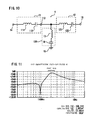
- Fig. 10 is a circuit diagram illustrating a band-pass filter 4 that is a modified example of the band-pass filter 1.
- the band-pass filter 4 is provided with a capacitor 16.
- the capacitor 16 is connected between the coil 13 and the ground 15.
- the coil 13 and the capacitor 16 compose a series resonance circuit 130.
- Fig. 11 is a Bode diagram illustrating a simulation result of a frequency characteristic (cutoff characteristic) of a gain of the band-pass filter 4.
- Fig. 12 is a graph illustrating a frequency characteristic of an input impedance of the band-pass filter 4.
- the values of the respective elements of the band-pass filter 1 are the same as the values set at the time of the simulation of the band-pass filter 1.
- a capacitance of the capacitor 16 is set to 56 pF.
- a resonant frequency of the series resonance circuit 130 (about 92 MHz) is included in the second band. That is to say, the series resonance circuit 130 functions as a notch filter.
- the resonant frequency of the series resonance circuit 130 is represented by f n
- the inductance of the coil 13 is represented by L 13
- the capacitance of the capacitor 16 is represented by C 16
- the resonant frequency f n is expressed by the following (Formula 16).
- the frequency characteristic of the gain of the band-pass filter 4 is steeper than the frequency characteristic of the gain of the band-pass filter 1.
Landscapes
- Engineering & Computer Science (AREA)
- Power Engineering (AREA)
- Filters And Equalizers (AREA)
Abstract
In a branch circuit (100), a first band-pass filter (1) allows a first band signal in an input signal to pass therethrough.
A second band-pass filter (2) allows a second band signal in the input signal to pass therethrough. The first band-pass filter has a pre-resonance (11) circuit, a post-resonance (12) circuit, and a coil (13). The pre-resonance circuit has a coil (111), and a capacitor (112) connected to the coil in series and is connected to an input terminal (14) of the first band-pass filter. The post-resonance circuit (12) has a coil (121), and a capacitor (122) connected to the coil in series, and is connected between the pre-resonance circuit and an output terminal (15) of the first band-pass filter. The coil (13) is connected between an output terminal (113) of the pre-resonance circuit and a ground.
A second band-pass filter (2) allows a second band signal in the input signal to pass therethrough. The first band-pass filter has a pre-resonance (11) circuit, a post-resonance (12) circuit, and a coil (13). The pre-resonance circuit has a coil (111), and a capacitor (112) connected to the coil in series and is connected to an input terminal (14) of the first band-pass filter. The post-resonance circuit (12) has a coil (121), and a capacitor (122) connected to the coil in series, and is connected between the pre-resonance circuit and an output terminal (15) of the first band-pass filter. The coil (13) is connected between an output terminal (113) of the pre-resonance circuit and a ground.
Description
- The present invention relates to a branch circuit, and more particularly to the branch circuit for separating a first band signal, and a second band signal different from the first band signal from an input signal.
- Branch circuits are circuits that separate signals in a plurality of frequency bands from an input signal. Use of the branch circuits enables a signal in a frequency band (174 to 240 MHz) of DAB (Digital Audio Broadcast) and a signal in a frequency band (76 to 108 MHz) of FM (Frequency Modulation) broadcasting to be separated from an input signal. The branch circuits have a band-pass filter for allowing signals in the frequency band of DAB to pass through, and a band-pass filter for allowing the signals in the frequency band of FM broadcasting to pass through. The band-pass filters are circuits for allowing signals in a desired band to pass through and attenuating signals other than ones in the desired band.
- Conventionally, band-pass filters using an operational amplifier are known. Further, resonator-coupling type band-pass filters using a parallel resonance circuit having a coil and a capacitor connected to the coil in parallel are known.
JP Patent publication 11-298202 - One of characteristics of the resonator-coupling type band-pass filters is a steep frequency characteristic. Use of the resonator-coupling type band-pass filter enables a narrow-band signal to be separated from an input signal.
- However, in the conventional resonator-coupling type band-pass filters, an input impedance in a pass band is higher than an input impedance in bands other than the pass band. In the resonator-coupling type band-pass filters, since the parallel resonance circuits are grounded, signals other than the pass band signal pass through the parallel resonance circuits so as to output to the ground. Therefore, when a first band signal and a second band signal are separated from an input signal, the use of the resonator-coupling type band-pass filters for passing of the first band signal causes an increase in loss of the second band signal.
- It is an object of the present invention to provide a branch circuit that can suppress an increase in loss of signals in respective bands when signals in a plurality of bands are separated from an input signal.
- A branch circuit of the present invention for separating a first band signal and a second band signal different from the first band signal from an input signal, comprises: a first band-pass filter for allowing the first band signal in the input signal to pass through; and a second band-pass filter for allowing the second band signal in the input signal to pass through. The first band-pass filter includes; a pre-resonance circuit having a first coil and a first capacitor connected to the first coil in series, the pre-resonance circuit being connected to an input terminal of the first band-pass filter, a post-resonance circuit having a second coil and a second capacitor connected to the second coil in series, and the post-resonance circuit being connected between the pre-resonance circuit and an output terminal of the first band-pass filter, and a third coil connected between the output terminal of the pre-resonance circuit and a ground.
- According to the present invention, an input impedance of a first band-pass filter in a first band becomes lower than an input impedance in bands other than the first band. Since the second band signal is prevented from being output to the ground via the first band-pass filter, the loss of the second band signal can be prevented.
- Preferably the first band-pass filter further includes a third capacitor connected between the third coil and the ground.
- As a result, a cutoff characteristic of the first band-pass filter in the first band can be made to be steep.
- Preferably when an impedance of the first band-pass filter is represented by ZL, a center frequency of the first band-pass filter is represented by f0, a bandwidth of the first band-pass filter is represented by Δf, and constants are represented by g1 and g2, an inductance Ls1 of the first coil and an inductance Ls2 of the second coil is expressed by the following (Formula 1), a capacitance Cs1 of the first capacitor and a capacitance Cs2 of the second capacitor are expressed by (Formula 2), and the inductance Lc of the third coil is expressed by (Formula 3).


- Use of the above (Formula 1), (Formula 2) and (Formula 3) enables parameters of respective elements composing the first band-pass filter to be determined.
-
-
Fig. 1 a circuit diagram illustrating a branch circuit according to an embodiment of the present invention; -
Fig. 2 is a circuit diagram illustrating a conventional low-pass filter; -
Fig. 3 is a Bode diagram illustrating a frequency characteristic of a gain of a resonator-coupling type band-pass filter shown inFig. 1 ; -
Fig. 4 is a graph illustrating a frequency characteristic of an input impedance of the resonator-coupling type band-pass filter shown inFig. 1 ; -
Fig. 5 is a Bode diagram illustrating a frequency characteristic of a gain of the branch circuit shown inFig. 1 ; -
Fig. 6 is a graph illustrating a frequency characteristic of an input impedance of the branch circuit shown inFig. 1 ; -
Fig. 7 is a circuit diagram illustrating a conventional resonator-coupling type band-pass filter; -
Fig. 8 is a Bode diagram illustrating a frequency characteristic of a gain of the resonator-coupling type band-pass filter shown inFig. 7 ; -
Fig. 9 is a graph illustrating a frequency characteristic of an input impedance of the resonator-coupling type band-pass filter shown inFig. 7 ; -
Fig. 10 is a circuit diagram illustrating a modified example of the resonator-coupling type band-pass filter shown inFig. 1 ; -
Fig. 11 is a Bode diagram illustrating a frequency characteristic of a gain of the band-pass filter shown inFig. 10 ; and -
Fig. 12 is a graph illustrating a frequency characteristic of an input impedance of the band-pass filter shown inFig. 10 . - An embodiment of the present invention will be described in detail below with reference to the drawings. Like members are denoted by like reference symbols in the drawings, and description thereof is not repeated. {Constitution of Branch Circuit}
-
Fig. 1 is a circuit diagram illustrating abranch circuit 100 according to the embodiment. With reference toFig. 1 , thebranch circuit 100 is provided with band-pass filters input terminal 101,output terminals pass filter 1 is connected between theinput terminal 101 and theoutput terminal 102. The band-pass filter 2 is connected between theinput terminal 101 and theoutput terminal 103. - The
branch circuit 100 inputs aninput signal 50 from theinput terminal 101. The band-pass filter 1 allows afirst band signal 51 in theinput signal 50 to pass through. Thefirst band signal 51 that passes through the band-pass filter 1 is output from theoutput terminal 102. The band-pass filter 2 allows asecond band signal 52 in theinput signal 50 to pass through. Thesecond band signal 52 that passes through the band-pass filter 2 is output from theoutput terminal 103. - For example, the first band is a frequency band (174 to 240 MHz) of DAB. The second band is a frequency band (76 to 108 MHz) of FM broadcasting. The first band and the second band are not limited to these frequency bands. The second band may be a frequency band higher than the first band or lower than the first band.
- A constitution of the
band pass filter 1 will be described. The band-pass filter 1 is a resonator-coupling type band-pass filter. The band-pass filter 1 has apre-resonance circuit 11, apost-resonance circuit 12, acoil 13, aninput terminal 14, and anoutput terminal 15. - The
pre-resonance circuit 11 is a series resonance circuit that has acoil 111, and acapacitor 112 connected to thecoil 111 in series. Thepre-resonance circuit 11 is connected to theinput terminal 14. Thepre-resonance circuit 11 further has theoutput terminal 113. One end of thecoil 111 is connected to theinput terminal 14, and the other end of thecoil 111 is connected to thecapacitor 112. Thecapacitor 112 is connected between thecoil 111 and theoutput terminal 113. - The
post-resonance circuit 12 is a series resonance circuit that has acoil 121, and acapacitor 122 connected to thecoil 121 in series. Thepost-resonance circuit 12 is connected between theoutput terminal 15 of thepre-resonance circuit 11 and theoutput terminal 113 of the band-pass filter 1. One end of thecoil 121 is connected to theoutput terminal 113, and the other end is connected to thecapacitor 122. Thecapacitor 122 is connected between thecoil 121 and theoutput terminal 15. - The
coil 13 is connected between theoutput terminal 113 and aground 15. - A constitution of the band-
pass filter 2 will be described. The band-pass filter 2 hascapacitors output terminal 26. - One end of the
capacitor 21 is connected to theinput terminal 101, and the other end of thecapacitor 21 is connected to one end of thecoil 22. The other end of thecoil 22 is connected to one end of thecapacitors 23. The other end of thecapacitors 23 is connected to theoutput terminal 26. Thecoil 24 is connected between the other end of thecapacitor 21 and aground 27. - The constitution of the band-
pass filter 2 is not limited to the above constitution. - The band-
pass filter 1 is a resonator-coupling type band-pass filter that has two series resonance circuits (thepre-resonance circuit 11 and the post-resonance circuit 12). In the band-pass filter 1, an input impedance in frequency bands other than the first band is higher than an input impedance in the first band. - For this reason, when the input impedance of the band-
pass filter 2 in the second band is lower than the input impedance of the band-pass filter 1 in the second band, thesecond band signal 52 included in theinput signal 50 is input into the band-pass filter 2. That is to say, thesecond band signal 52 can be prevented from passing through thepre-resonance circuit 11 and thecoil 13 and being output to theground 15. Therefore, thebranch circuit 100 can prevent loss of thesecond band signal 52 and can separate thefirst band signal 51 and thesecond band signal 52 from theinput signal 50. - A relationship among the elements composing the band-
pass filter 1 will be described. A resonance frequency of thepre-resonance circuit 11 matches with a resonance frequency of thepost-resonance circuit 12. As a result, a frequency characteristic of a steep gain can be obtained. - Further, an inductance of the
coil 111 matches with an inductance of thecoil 121. In this case, a capacitance of thecapacitor 112 matches with a capacitance of thecapacitor 122. When not match, a center frequency of the resonance circuit composed of thepre-resonance circuit 11 and thecoil 13 deviates from a center frequency of the resonance circuit composed of thepost-resonance circuit 12 and thecoil 13. As a result, since a bandwidth of the band-pass filter 1 is widened, the frequency characteristic of a steep gain cannot be obtained. - A method for calculating values of the respective elements composing the band-
pass filter 1 will be described. In the calculation of the values of the elements, values of the elements of a normalization low-pass filter having the Butterworth characteristic are used. -
Fig. 2 is a circuit diagram illustrating a normalization low-pass filter 60. The normalization low-pass filter 60 has a coil 61, acapacitor 62, aninput terminal 63, and anoutput terminal 64. One end of the coil 61 is connected to theinput terminal 63, and the other end of the coil 61 is connected to theoutput terminal 64. Thecapacitor 62 is connected between the other end of the coil 61 and aground 65. - In the normalization low-
pass filter 60, an impedance is 1 Ω. A cutoff frequency is (1/2π) Hz. Therefore, an inductance of the coil 61 is 1.41421 H. A capacitance of thecapacitor 62 is 1.41421 F. - The center frequency, the bandwidth, and the impedance of the band-
pass filter 1 are represented by f0, Δf, and ZL. The values of thecoils capacitors 112 and 114 are calculated by using these parameters. - At first, constants g1 and g2 are defined based on the inductance of the coil 61 and the capacitance of the
capacitor 62 as expressed by the following (Formula 4).
- The constants g1 and g2 match with the value of the coil 61 or the
capacitor 62 of the normalization low-pass filter 60. A normalization coupling constant k12 is defined by using the constants g1 and g2 according to the following (Formula 5).
- A constant K12 is defined by using the normalization coupling constant k12 according to the following (Formula 6).

- The constant K12 is a numerical value such that the normalization coupling constant k12 is changed according to the center frequency f0 and the bandwidth Δf. The constant K12 is a characteristic value of a coupled circuit where the
pre-resonance circuit 11 is coupled with thepost-resonance circuit 12. In this embodiment, the coupled circuit corresponds to thecoil 13. - Provisional values (hereinafter, called provisional capacitances) of capacitances of the
capacitors coils 111 and 121 (hereinafter, "provisional inductance") Lt1 are calculated by using the following (Formula 7). The provisional inductances Lt1 are calculated as the inductances of the coils resonating with the provisional capacitances Ct1.
- A provisional value of the inductance of the coupled circuit (the coil 13) (hereinafter, "provisional coupled inductance") Lct is calculated according to the following (Formula 8).

- As expressed in the following (Formula 9), the inductance Lct of the
coil 13 is subtracted from the provisional inductance Lt1 of thecoils coil 111 resonates with thecapacitor 112. Further, the coupled circuit (the coil 13) as well as thecoil 121 resonates with thecapacitor 122. For this reason, when thecoils pass filter 1 deviates from f0. The provisional inductances Lt1 are adjusted by using the following (Formula 9) so that the deviation does not occur. As a result, the provisional inductances Lt2 of thecoils 
- Next, Impedance conversion is made. The provisional capacitances Ct1, the provisional inductances Lt2, and the provisional coupled inductances Lct are changed according to the input impedance RL of the band-
pass filter 1. - An input impedance Z1 and an output impedance Z2 of the band-
pass filter 1 are calculated by using the following (Formula 10) and (Formula 11).

- Since it is assumed that the normalization low-
pass filter 60 has the Butterworth characteristic, the input impedance Z1 and the output impedance Z2 have the same value. Further, since the input impedance Z1 and the output impedance Z2 include the provisional capacitance Ct1, they correspond to a provisional value of the impedance of the band-pass filter 1. - A ratio R between the impedance RL of the band-
pass filter 1 and the impedance Z1 is calculated by using the following (Formula 12).
- As expressed in the following (Formula 13), the provisional inductance Lt2 is multiplied by the ratio R, so that an inductance Ls1 of the
coil 111 and an inductances Ls2 of thecoil 121 are obtained.
- As expressed in the following (Formula 14), the provisional capacitance Ct1 is multiplied by an inverse of the ratio R, so that a capacitance Cs1 of the
capacitor 112 and a capacitance Cs2 of thecapacitor 122 are obtained.
- In the band-
pass filter 1, the coupled circuit is composed of thecoil 13. Therefore, an inductance Lc of thecoil 13 is calculated by multiplying the provisional coupled inductance Lct by the ratio R as expressed in the following (Formula 15).
- As described above, g1 and g2 are constants. Therefore, it is found that the inductances Lc, Ls1 and Ls2 of the
coils capacitors pass filter 1. - The frequency characteristic of the band-
pass filter 1 will be described below. Parameters of the band-pass filter 1 were set, and the frequency characteristic of the band-pass filter 1 was simulated. - Before the simulation, the center frequency f0, the bandwidth Δf and the impedance ZL of the band-
pass filter 1 were set to 207 MHz, 105 MHz and 75 Ω. The inductances Ls1 and Ls2 of thecoils capacitors coil 13 was set to 57.66 nH. -
Fig. 3 is a Bode diagram illustrating a simulated result of the frequency characteristic (cutoff characteristic) of the gain in the band-pass filter 1.Fig. 4 is a graph illustrating a simulation result of the frequency characteristic of the input impedance in the band-pass filter 1. - With reference to
Fig. 3 , the gain of the band-pass filter 1 has a peak in the first band (174 to 240 MHz). With reference toFig. 4 , the input impedance of the band-pass filter 1 reduces from the center frequency f0 (207 MHz). That is to say, the input impedance in the first band is lower than the input impedances in bands other than the first band. - A frequency characteristic of the
branch circuit 100 was simulated.Fig. 5 is a Bode diagram illustrating a simulated result of the frequency characteristic (cutoff characteristic) of the gain of thebranch circuit 100.Fig. 6 is a graph illustrating a simulated result of a frequency characteristic of the input impedance of thebranch circuit 100. - In the simulation of the
branch circuit 100, the values of the respective elements of the band-pass filter 1 are the same as the values set at the time of the simulation of the band-pass filter 1. In the band-pass filter 2, the capacitance of thecapacitor 21 was set to 18 pF, and the capacitance of thecapacitors 23 was set to 5.6 pF. A reactance of thecoil 22 was set to 560 mH, and a reactance of thecoil 24 was set to 270 mH. - With reference to
Fig. 5 , acurved line 71 corresponds to the frequency characteristic of the gain of the band-pass filter 1, and acurved line 72 corresponds to the frequency characteristic of the gain of the band-pass filter 2. Since the peak is present in the first band and the second band, it is found that thebranch circuit 100 can separate thefirst band signal 51 and thesecond band signal 52 from theinput signal 50. - With reference to
Fig. 6 , acurved line 81 corresponds to the frequency characteristic of the input impedance of the band-pass filter 1. Acurved line 82 corresponds to the frequency characteristic of the input impedance of the band-pass filter 2. In the first band, the input impedance of the band-pass filter 1 is lower than the input impedance of the band-pass filter 2. Therefore, thefirst band signal 51 is input into the band-pass filter 1. On the other hand, in the second band, the input impedance of the band-pass filter 2 is lower than the input impedance of the band-pass filter 1. Therefore, thesecond band signal 52 is input into the band-pass filter 2. - As a result, the
second band signal 52 is prevented from being output to theground 15 via the band-pass filter 1. Therefore, a loss of thesecond band signal 52 to be caused from the band-pass filter 1 can be prevented. - As a comparative example, a simulation result of a conventional resonator-coupling type band-pass filter will be described below.
Fig. 7 is a circuit diagram illustrating the conventional resonator-coupling type band-pass filter. A band-pass filter 3 shown inFig. 7 is provided withcapacitors input terminal 36, and anoutput terminal 37. - One end of the
capacitor 31 is connected to theinput terminal 36, and the other end of thecapacitor 31 is connected to theoutput terminal 37. One end of thecoil 32 is connected to theinput terminal 36, and the other end of thecoil 32 is grounded. One end of the capacitor 33 is connected to theinput terminal 36, and the other end of the capacitor 33 is grounded. That is to say, the capacitor 33 is connected to thecoil 32 in parallel. One end of thecoil 34 is connected to the other end of thecapacitor 31, and the other end of thecoil 34 is grounded. One end of thecapacitor 35 is connected to the other end of thecapacitor 31, and the other end of thecapacitor 35 is grounded. That is to say, thecapacitor 35 is connected to thecoil 34 in parallel. -
Fig. 8 is a Bode diagram illustrating a simulation result of a frequency characteristic (cutoff characteristic) of a gain of the band-pass filter 3.Fig. 9 is a graph illustrating a simulation result of a frequency characteristic of an input impedance of the band-pass filter 3. The center frequency f0, the bandwidth Δf and the impedance ZL of the band-pass filter 3 were set to the same values of the band-pass filter 1. A capacitance of thecapacitor 31 was set to 10.25 pF, and capacitances of thecapacitors 33 and 35 were set to 18.32 pF. Inductances of thecoils - With reference to
Fig. 3 andFig. 8 , the frequency characteristic of the gain of the band-pass filter 1 matches with the frequency characteristic of the gain of the band-pass filter 2. - With reference to
Fig. 4 andFig. 9 , the frequency characteristic of the input impedance of the band-pass filter 3 is opposite to the frequency characteristic of the input impedance of the band-pass filter 1. That is to say, in the band-pass filter 3, the input impedance in the first band is higher than input impedances in bands other than the first band. - Therefore, in the
branch circuit 100, when the band-pass filter 1 is replaced by the band-pass filter 3, the following problem arises. When the input impedance of the band-pass filter 2 in the second band is higher than the input impedance of the band-pass filter 3 in the second band, the second band signal is output to the ground via the band-pass filter 3. Since the second band signal is not input into the band-pass filter 2, a loss of the second band signal increases. -
Fig. 10 is a circuit diagram illustrating a band-pass filter 4 that is a modified example of the band-pass filter 1. With reference toFig. 10 , in addition to the constitution of the band-pass filter 1, the band-pass filter 4 is provided with a capacitor 16. The capacitor 16 is connected between thecoil 13 and theground 15. Thecoil 13 and the capacitor 16 compose aseries resonance circuit 130. -
Fig. 11 is a Bode diagram illustrating a simulation result of a frequency characteristic (cutoff characteristic) of a gain of the band-pass filter 4.Fig. 12 is a graph illustrating a frequency characteristic of an input impedance of the band-pass filter 4. The values of the respective elements of the band-pass filter 1 are the same as the values set at the time of the simulation of the band-pass filter 1. A capacitance of the capacitor 16 is set to 56 pF. - With reference to
Fig. 11 , attenuation in the second band noticeably increases. This is because a resonant frequency of the series resonance circuit 130 (about 92 MHz) is included in the second band. That is to say, theseries resonance circuit 130 functions as a notch filter. When the resonant frequency of theseries resonance circuit 130 is represented by fn, the inductance of thecoil 13 is represented by L13, and the capacitance of the capacitor 16 is represented by C16, the resonant frequency fn is expressed by the following (Formula 16).
- With reference to
Fig. 3 andFig. 11 , the frequency characteristic of the gain of the band-pass filter 4 is steeper than the frequency characteristic of the gain of the band-pass filter 1. - With reference to
Fig. 4 andFig. 12 , there is no great difference between the frequency characteristic of the input impedance of the band-pass filter 1 and the frequency characteristic of the input impedance of the band-pass filter 4. Therefore, also in thebranch circuit 100, even when the band-pass filter 1 is replaced by the band-pass filter 4, the loss of the second band signal due to the band-pass filter 4 can be prevented, and thefirst band signal 51 and thesecond band signal 52 can be separated from theinput signal 50. - The above described the embodiment of the present invention, but the above embodiment is only example for carrying out the present invention. Therefore, the present invention is not limited to the above embodiment, and can be carried out by suitably modifying the above embodiment within the scope that does not deviate from the gist.
Claims (3)
- A branch circuit for separating a first band signal and a second band signal different from the first band signal from an input signal, comprising:a first band-pass filter for allowing the first band signal in the input signal to pass through; anda second band-pass filter for allowing the second band signal in the input signal to pass through,wherein the first band-pass filter includes;
a pre-resonance circuit having a first coil and a first capacitor connected to the first coil in series, the pre-resonance circuit being connected to an input terminal of the first band-pass filter,
a post-resonance circuit having a second coil and a second capacitor connected to the second coil in series, and the post-resonance circuit being connected between the pre-resonance circuit and an output terminal of the first band-pass filter, and
a third coil connected between the output terminal of the pre-resonance circuit and a ground. - The branch circuit according to claim 1, wherein the first band-pass filter further includes a third capacitor connected between the third coil and the ground.
- The branch circuit according to claim 1 or 2, wherein
when an impedance of the first band-pass filter is represented by ZL, a center frequency of the first band-pass filter is represented by f0, a bandwidth of the first band-pass filter is represented by Δf, and constants are represented by g1 and g2, an inductance Ls1 of the first coil and an inductance Ls2 of the second coil is expressed by the following (Formula 1),
a capacitance Cs1 of the first capacitor and a capacitance Cs2 of the second capacitor are expressed by (Formula 2), and
the inductance Lc of the third coil is expressed by (Formula 3).

Applications Claiming Priority (1)
| Application Number | Priority Date | Filing Date | Title |
|---|---|---|---|
| JP2011212677A JP2013074496A (en) | 2011-09-28 | 2011-09-28 | Branch circuit |
Publications (1)
| Publication Number | Publication Date |
|---|---|
| EP2575253A1 true EP2575253A1 (en) | 2013-04-03 |
Family
ID=46022007
Family Applications (1)
| Application Number | Title | Priority Date | Filing Date |
|---|---|---|---|
| EP12162033A Withdrawn EP2575253A1 (en) | 2011-09-28 | 2012-03-29 | Branch ciruit |
Country Status (2)
| Country | Link |
|---|---|
| EP (1) | EP2575253A1 (en) |
| JP (1) | JP2013074496A (en) |
Cited By (6)
| Publication number | Priority date | Publication date | Assignee | Title |
|---|---|---|---|---|
| CN104348441A (en) * | 2013-07-23 | 2015-02-11 | Tdk株式会社 | Diplexer including two bandpass filters |
| CN105959029A (en) * | 2016-06-22 | 2016-09-21 | 东南大学 | Signal separation circuit based on time-varying aliasing filter and auxiliary circuits |
| CN106712517A (en) * | 2015-11-12 | 2017-05-24 | 华为技术有限公司 | Resonant bidirectional conversion circuit and converter |
| CN107017856A (en) * | 2016-01-25 | 2017-08-04 | Tdk株式会社 | Bandpass filter and channel-splitting filter |
| CN107888158A (en) * | 2017-11-07 | 2018-04-06 | 福建北峰通信科技股份有限公司 | A kind of electric tuning radio frequency band filter circuit |
| CN111464140A (en) * | 2020-05-26 | 2020-07-28 | 深圳市前海派速科技有限公司 | Power amplifier with filtering function, 5G communication device and 5G communication system |
Families Citing this family (1)
| Publication number | Priority date | Publication date | Assignee | Title |
|---|---|---|---|---|
| WO2022196642A1 (en) * | 2021-03-16 | 2022-09-22 | 株式会社村田製作所 | Transient voltage absorbing circuit |
Citations (7)
| Publication number | Priority date | Publication date | Assignee | Title |
|---|---|---|---|---|
| US2358520A (en) * | 1939-10-28 | 1944-09-19 | Rca Corp | Coupling transformer |
| US2762018A (en) * | 1950-10-09 | 1956-09-04 | John Hays Hammond Jr | Reactance networks with structural symmetry |
| DE1003823B (en) * | 1955-06-21 | 1957-03-07 | Deutsche Bundespost | Switching arrangement for radio stations equipped with antenna switches for two-way communication on different frequencies |
| DE1084783B (en) * | 1959-04-24 | 1960-07-07 | Siemens Ag | Distribution or antenna switch for the reception of several television channels |
| JPS6113706A (en) * | 1984-06-28 | 1986-01-22 | Matsushita Electric Ind Co Ltd | band pass filter |
| EP0921642A2 (en) * | 1997-12-03 | 1999-06-09 | Hitachi Metals, Ltd. | Multiband high-frequency switching module |
| JPH11298202A (en) | 1998-04-09 | 1999-10-29 | Murata Mfg Co Ltd | Band pass filter and double multiplication circuit |
Family Cites Families (7)
| Publication number | Priority date | Publication date | Assignee | Title |
|---|---|---|---|---|
| JPS5015339B1 (en) * | 1969-10-24 | 1975-06-04 | ||
| JPS5016447A (en) * | 1973-06-08 | 1975-02-21 | ||
| JPS6490601A (en) * | 1987-09-30 | 1989-04-07 | Sumitomo Electric Industries | Frequency channel branching filter |
| DE9205615U1 (en) * | 1992-04-25 | 1992-07-02 | Robert Bosch Gmbh, 7000 Stuttgart | Vehicle antenna splitter |
| US6101371A (en) * | 1998-09-12 | 2000-08-08 | Lucent Technologies, Inc. | Article comprising an inductor |
| JP2002280862A (en) * | 2001-03-19 | 2002-09-27 | Murata Mfg Co Ltd | Composite lc filter circuit and composite lc filter component |
| JP4105726B2 (en) * | 2006-01-31 | 2008-06-25 | 日本電業工作株式会社 | Band stop filter |
-
2011
- 2011-09-28 JP JP2011212677A patent/JP2013074496A/en active Pending
-
2012
- 2012-03-29 EP EP12162033A patent/EP2575253A1/en not_active Withdrawn
Patent Citations (7)
| Publication number | Priority date | Publication date | Assignee | Title |
|---|---|---|---|---|
| US2358520A (en) * | 1939-10-28 | 1944-09-19 | Rca Corp | Coupling transformer |
| US2762018A (en) * | 1950-10-09 | 1956-09-04 | John Hays Hammond Jr | Reactance networks with structural symmetry |
| DE1003823B (en) * | 1955-06-21 | 1957-03-07 | Deutsche Bundespost | Switching arrangement for radio stations equipped with antenna switches for two-way communication on different frequencies |
| DE1084783B (en) * | 1959-04-24 | 1960-07-07 | Siemens Ag | Distribution or antenna switch for the reception of several television channels |
| JPS6113706A (en) * | 1984-06-28 | 1986-01-22 | Matsushita Electric Ind Co Ltd | band pass filter |
| EP0921642A2 (en) * | 1997-12-03 | 1999-06-09 | Hitachi Metals, Ltd. | Multiband high-frequency switching module |
| JPH11298202A (en) | 1998-04-09 | 1999-10-29 | Murata Mfg Co Ltd | Band pass filter and double multiplication circuit |
Non-Patent Citations (1)
| Title |
|---|
| CHIU C T ET AL: "Bandpass Filters Design in the Organic Substrate without Using Large-Value Capacitors", MICROSYSTEMS, PACKAGING, ASSEMBLY CONFERENCE TAIWAN, 2006 INTERNATIONA L, IEEE, PI, 1 October 2006 (2006-10-01), pages 1 - 4, XP031049544, ISBN: 978-1-4244-0734-7 * |
Cited By (9)
| Publication number | Priority date | Publication date | Assignee | Title |
|---|---|---|---|---|
| CN104348441A (en) * | 2013-07-23 | 2015-02-11 | Tdk株式会社 | Diplexer including two bandpass filters |
| US9413328B2 (en) | 2013-07-23 | 2016-08-09 | Tdk Corporation | Diplexer including two bandpass filters |
| CN104348441B (en) * | 2013-07-23 | 2017-06-13 | Tdk株式会社 | Duplexer |
| CN106712517A (en) * | 2015-11-12 | 2017-05-24 | 华为技术有限公司 | Resonant bidirectional conversion circuit and converter |
| CN107017856A (en) * | 2016-01-25 | 2017-08-04 | Tdk株式会社 | Bandpass filter and channel-splitting filter |
| CN107017856B (en) * | 2016-01-25 | 2020-07-10 | Tdk株式会社 | Band-pass filter and branching filter |
| CN105959029A (en) * | 2016-06-22 | 2016-09-21 | 东南大学 | Signal separation circuit based on time-varying aliasing filter and auxiliary circuits |
| CN107888158A (en) * | 2017-11-07 | 2018-04-06 | 福建北峰通信科技股份有限公司 | A kind of electric tuning radio frequency band filter circuit |
| CN111464140A (en) * | 2020-05-26 | 2020-07-28 | 深圳市前海派速科技有限公司 | Power amplifier with filtering function, 5G communication device and 5G communication system |
Also Published As
| Publication number | Publication date |
|---|---|
| JP2013074496A (en) | 2013-04-22 |
Similar Documents
| Publication | Publication Date | Title |
|---|---|---|
| KR101321772B1 (en) | Resonator and filter using thereof in a communication system | |
| US20160218695A1 (en) | Ladder filter | |
| US10554195B2 (en) | Band-pass filter and branching filter | |
| US10439582B2 (en) | Variable-frequency LC filter, high-frequency frontend module, and communication apparatus | |
| JP5673818B2 (en) | Duplexer | |
| US10651821B2 (en) | Multiplexer, high-frequency front-end circuit, and communication apparatus | |
| JP6308221B2 (en) | Variable frequency filter | |
| US20180241368A1 (en) | Multi-harmonic matching networks | |
| DE20222017U1 (en) | Two-channel passband filter system using acoustic resonators in grating topology | |
| US12567855B2 (en) | System and method for coupled resonator filtering | |
| JP2013074496A (en) | Branch circuit | |
| US12273089B2 (en) | Integrated circuit comprising an adaptation and filtering network and corresponding adaptation and filtering process | |
| JP2021500838A5 (en) | ||
| US20210099159A1 (en) | Multiplexer | |
| US10090824B2 (en) | Filter apparatus | |
| CN108028641B (en) | Frequency variable filter, high frequency front-end circuit | |
| EP0203343B1 (en) | Trap circuit with two variable inductors | |
| US20210152155A1 (en) | Composite filter device | |
| KR20210081257A (en) | Composite filter device and band pass filter | |
| JPH08274504A (en) | Filter device for high frequency | |
| JP6703852B2 (en) | Variable bandpass filter | |
| JP4813984B2 (en) | Low pass filter | |
| JP6994988B2 (en) | Filters and electronic devices | |
| RU168664U1 (en) | BANDFILTER LC FILTER SUPPRESSED WITH FOCUSED INTERFERENCE IN THE FREQUENCY WORKBAND | |
| CN108920762A (en) | A kind of filter circuit |
Legal Events
| Date | Code | Title | Description |
|---|---|---|---|
| PUAI | Public reference made under article 153(3) epc to a published international application that has entered the european phase |
Free format text: ORIGINAL CODE: 0009012 |
|
| AK | Designated contracting states |
Kind code of ref document: A1 Designated state(s): AL AT BE BG CH CY CZ DE DK EE ES FI FR GB GR HR HU IE IS IT LI LT LU LV MC MK MT NL NO PL PT RO RS SE SI SK SM TR |
|
| AX | Request for extension of the european patent |
Extension state: BA ME |
|
| STAA | Information on the status of an ep patent application or granted ep patent |
Free format text: STATUS: THE APPLICATION IS DEEMED TO BE WITHDRAWN |
|
| 18D | Application deemed to be withdrawn |
Effective date: 20131005 |