EP2575416B1 - A device having wirelessly enabled functional blocks - Google Patents
A device having wirelessly enabled functional blocks Download PDFInfo
- Publication number
- EP2575416B1 EP2575416B1 EP12005675.9A EP12005675A EP2575416B1 EP 2575416 B1 EP2575416 B1 EP 2575416B1 EP 12005675 A EP12005675 A EP 12005675A EP 2575416 B1 EP2575416 B1 EP 2575416B1
- Authority
- EP
- European Patent Office
- Prior art keywords
- substrate
- wirelessly enabled
- enabled functional
- ground ring
- pcb
- Prior art date
- Legal status (The legal status is an assumption and is not a legal conclusion. Google has not performed a legal analysis and makes no representation as to the accuracy of the status listed.)
- Active
Links
Images


Classifications
-
- H—ELECTRICITY
- H05—ELECTRIC TECHNIQUES NOT OTHERWISE PROVIDED FOR
- H05K—PRINTED CIRCUITS; CASINGS OR CONSTRUCTIONAL DETAILS OF ELECTRIC APPARATUS; MANUFACTURE OF ASSEMBLAGES OF ELECTRICAL COMPONENTS
- H05K1/00—Printed circuits
-
- H—ELECTRICITY
- H10—SEMICONDUCTOR DEVICES; ELECTRIC SOLID-STATE DEVICES NOT OTHERWISE PROVIDED FOR
- H10W—GENERIC PACKAGES, INTERCONNECTIONS, CONNECTORS OR OTHER CONSTRUCTIONAL DETAILS OF DEVICES COVERED BY CLASS H10
- H10W42/00—Arrangements for protection of devices
- H10W42/20—Arrangements for protection of devices protecting against electromagnetic or particle radiation, e.g. light, X-rays, gamma-rays or electrons
-
- H—ELECTRICITY
- H10—SEMICONDUCTOR DEVICES; ELECTRIC SOLID-STATE DEVICES NOT OTHERWISE PROVIDED FOR
- H10W—GENERIC PACKAGES, INTERCONNECTIONS, CONNECTORS OR OTHER CONSTRUCTIONAL DETAILS OF DEVICES COVERED BY CLASS H10
- H10W44/00—Electrical arrangements for controlling or matching impedance
- H10W44/20—Electrical arrangements for controlling or matching impedance at high-frequency [HF] or radio frequency [RF]
-
- H—ELECTRICITY
- H10—SEMICONDUCTOR DEVICES; ELECTRIC SOLID-STATE DEVICES NOT OTHERWISE PROVIDED FOR
- H10W—GENERIC PACKAGES, INTERCONNECTIONS, CONNECTORS OR OTHER CONSTRUCTIONAL DETAILS OF DEVICES COVERED BY CLASS H10
- H10W70/00—Package substrates; Interposers; Redistribution layers [RDL]
- H10W70/60—Insulating or insulated package substrates; Interposers; Redistribution layers
- H10W70/62—Insulating or insulated package substrates; Interposers; Redistribution layers characterised by their interconnections
- H10W70/65—Shapes or dispositions of interconnections
- H10W70/657—Shapes or dispositions of interconnections on sidewalls or bottom surfaces of the package substrates, interposers or redistribution layers
-
- H—ELECTRICITY
- H10—SEMICONDUCTOR DEVICES; ELECTRIC SOLID-STATE DEVICES NOT OTHERWISE PROVIDED FOR
- H10W—GENERIC PACKAGES, INTERCONNECTIONS, CONNECTORS OR OTHER CONSTRUCTIONAL DETAILS OF DEVICES COVERED BY CLASS H10
- H10W72/00—Interconnections or connectors in packages
-
- H—ELECTRICITY
- H10—SEMICONDUCTOR DEVICES; ELECTRIC SOLID-STATE DEVICES NOT OTHERWISE PROVIDED FOR
- H10W—GENERIC PACKAGES, INTERCONNECTIONS, CONNECTORS OR OTHER CONSTRUCTIONAL DETAILS OF DEVICES COVERED BY CLASS H10
- H10W90/00—Package configurations
-
- H—ELECTRICITY
- H10—SEMICONDUCTOR DEVICES; ELECTRIC SOLID-STATE DEVICES NOT OTHERWISE PROVIDED FOR
- H10W—GENERIC PACKAGES, INTERCONNECTIONS, CONNECTORS OR OTHER CONSTRUCTIONAL DETAILS OF DEVICES COVERED BY CLASS H10
- H10W90/00—Package configurations
- H10W90/20—Configurations of stacked chips
- H10W90/293—Configurations of stacked chips characterised by non-galvanic coupling between the chips, e.g. capacitive coupling
-
- H—ELECTRICITY
- H10—SEMICONDUCTOR DEVICES; ELECTRIC SOLID-STATE DEVICES NOT OTHERWISE PROVIDED FOR
- H10W—GENERIC PACKAGES, INTERCONNECTIONS, CONNECTORS OR OTHER CONSTRUCTIONAL DETAILS OF DEVICES COVERED BY CLASS H10
- H10W44/00—Electrical arrangements for controlling or matching impedance
- H10W44/20—Electrical arrangements for controlling or matching impedance at high-frequency [HF] or radio frequency [RF]
- H10W44/241—Electrical arrangements for controlling or matching impedance at high-frequency [HF] or radio frequency [RF] for passive devices or passive elements
- H10W44/248—Electrical arrangements for controlling or matching impedance at high-frequency [HF] or radio frequency [RF] for passive devices or passive elements for antennas
-
- H—ELECTRICITY
- H10—SEMICONDUCTOR DEVICES; ELECTRIC SOLID-STATE DEVICES NOT OTHERWISE PROVIDED FOR
- H10W—GENERIC PACKAGES, INTERCONNECTIONS, CONNECTORS OR OTHER CONSTRUCTIONAL DETAILS OF DEVICES COVERED BY CLASS H10
- H10W72/00—Interconnections or connectors in packages
- H10W72/20—Bump connectors, e.g. solder bumps or copper pillars; Dummy bumps; Thermal bumps
- H10W72/251—Materials
- H10W72/252—Materials comprising solid metals or solid metalloids, e.g. PbSn, Ag or Cu
-
- H—ELECTRICITY
- H10—SEMICONDUCTOR DEVICES; ELECTRIC SOLID-STATE DEVICES NOT OTHERWISE PROVIDED FOR
- H10W—GENERIC PACKAGES, INTERCONNECTIONS, CONNECTORS OR OTHER CONSTRUCTIONAL DETAILS OF DEVICES COVERED BY CLASS H10
- H10W72/00—Interconnections or connectors in packages
- H10W72/20—Bump connectors, e.g. solder bumps or copper pillars; Dummy bumps; Thermal bumps
- H10W72/29—Bond pads specially adapted therefor
-
- H—ELECTRICITY
- H10—SEMICONDUCTOR DEVICES; ELECTRIC SOLID-STATE DEVICES NOT OTHERWISE PROVIDED FOR
- H10W—GENERIC PACKAGES, INTERCONNECTIONS, CONNECTORS OR OTHER CONSTRUCTIONAL DETAILS OF DEVICES COVERED BY CLASS H10
- H10W72/00—Interconnections or connectors in packages
- H10W72/30—Die-attach connectors
- H10W72/351—Materials of die-attach connectors
- H10W72/353—Materials of die-attach connectors not comprising solid metals or solid metalloids, e.g. ceramics
- H10W72/354—Materials of die-attach connectors not comprising solid metals or solid metalloids, e.g. ceramics comprising polymers
-
- H—ELECTRICITY
- H10—SEMICONDUCTOR DEVICES; ELECTRIC SOLID-STATE DEVICES NOT OTHERWISE PROVIDED FOR
- H10W—GENERIC PACKAGES, INTERCONNECTIONS, CONNECTORS OR OTHER CONSTRUCTIONAL DETAILS OF DEVICES COVERED BY CLASS H10
- H10W72/00—Interconnections or connectors in packages
- H10W72/90—Bond pads, in general
- H10W72/941—Dispositions of bond pads
- H10W72/9415—Dispositions of bond pads relative to the surface, e.g. recessed, protruding
-
- H—ELECTRICITY
- H10—SEMICONDUCTOR DEVICES; ELECTRIC SOLID-STATE DEVICES NOT OTHERWISE PROVIDED FOR
- H10W—GENERIC PACKAGES, INTERCONNECTIONS, CONNECTORS OR OTHER CONSTRUCTIONAL DETAILS OF DEVICES COVERED BY CLASS H10
- H10W74/00—Encapsulations, e.g. protective coatings
- H10W74/10—Encapsulations, e.g. protective coatings characterised by their shape or disposition
- H10W74/15—Encapsulations, e.g. protective coatings characterised by their shape or disposition on active surfaces of flip-chip devices, e.g. underfills
-
- H—ELECTRICITY
- H10—SEMICONDUCTOR DEVICES; ELECTRIC SOLID-STATE DEVICES NOT OTHERWISE PROVIDED FOR
- H10W—GENERIC PACKAGES, INTERCONNECTIONS, CONNECTORS OR OTHER CONSTRUCTIONAL DETAILS OF DEVICES COVERED BY CLASS H10
- H10W90/00—Package configurations
- H10W90/701—Package configurations characterised by the relative positions of pads or connectors relative to package parts
- H10W90/721—Package configurations characterised by the relative positions of pads or connectors relative to package parts of bump connectors
- H10W90/724—Package configurations characterised by the relative positions of pads or connectors relative to package parts of bump connectors between a chip and a stacked insulating package substrate, interposer or RDL
-
- H—ELECTRICITY
- H10—SEMICONDUCTOR DEVICES; ELECTRIC SOLID-STATE DEVICES NOT OTHERWISE PROVIDED FOR
- H10W—GENERIC PACKAGES, INTERCONNECTIONS, CONNECTORS OR OTHER CONSTRUCTIONAL DETAILS OF DEVICES COVERED BY CLASS H10
- H10W90/00—Package configurations
- H10W90/701—Package configurations characterised by the relative positions of pads or connectors relative to package parts
- H10W90/731—Package configurations characterised by the relative positions of pads or connectors relative to package parts of die-attach connectors
- H10W90/734—Package configurations characterised by the relative positions of pads or connectors relative to package parts of die-attach connectors between a chip and a stacked insulating package substrate, interposer or RDL
Definitions
- the present invention generally relates to integrated circuit (IC) devices, and more particularly to communications involving IC devices.
- IC integrated circuit
- Integrated circuit (IC) devices typically include an IC die housed in a package.
- the IC device can be coupled to a printed circuit board (PCB) to enable communication between the IC device and other devices coupled to the PCB.
- PCB printed circuit board
- an IC die is often coupled to a substrate, which is coupled to an array of connection elements, e.g., an array of solder balls. The array of connections elements is then physically coupled to the PCB.
- An IC die can be coupled to a substrate in a variety of ways. For example, in die-down flip-chip packages, solder bumps can be used to couple contact pads on a surface of the IC die to contact pads located on the substrate. In another example, wirebonds can be used to couple bond pads on a surface of the IC die to bond fingers located on the substrate.
- US 2009/0266900 A1 discloses a wireless IC device with a wireless IC that processes transmission and reception signals, wherein a feeder circuit incorporates an inductance element connected to the wireless IC in a galvanically conductive state and in which a feeder electrode coupled to the inductance element is provided on a surface of the substrate or an inside of the substrate, and a radiation plate is electromagnetically coupled to the feeder electrode.
- an integrated circuit (IC) device is provided according to the attached independent claim 1.
- the ground ring comprises a metal trace formed on the surface of the substrate.
- the IC device further comprises:
- the IC device is configured to be coupled to a printed circuit board (PCB) and wherein the ground ring is coupled to the PCB.
- PCB printed circuit board
- the ground ring comprises a flexible material.
- the IC device further comprises a coupling member configured to couple the ground ring to the substrate.
- the coupling member is configured to allow for the substrate to move independently of the ground ring.
- the IC device further comprises a second ground ring located on the surface of the substrate.
- the IC device is configured to be coupled to a surface of a printed circuit board (PCB), the IC device further comprising:
- the ground ring is configured to provide electromagnetic shielding for the third and fourth wirelessly enabled functional blocks.
- the IC device further comprises a solder ball coupled to the second surface of the substrate that is configured to be coupled to the surface of the PCB.
- a method of assembling an integrated circuit (IC) device is provided according to the attached independent claim 15.
- the method further comprises:
- the method further comprises:
- references in the specification to "one embodiment”, “an embodiment”, “an example embodiment”, etc., indicate that the embodiment described may include a particular feature, structure, or characteristic, but every embodiment may not necessarily include the particular feature, structure, or characteristic. Moreover, such phrases are not necessarily referring to the same embodiment. Further, when a particular feature, structure, or characteristic is described in connection with an embodiment, it is submitted that it is within the knowledge of one skilled in the art to effect such feature, structure, or characteristic in connection with other embodiments whether or not explicitly described.
- FIG. 1 shows a cross-sectional view of a conventional die down ball grid array (BGA) package 100.
- BGA package 100 includes an IC die 110 coupled to a top surface 125 of a substrate 120 via solder bumps 130.
- BGA package 100 is a die down package in which an active surface 115 of die 110 faces substrate 120. On the other hand, in die up packages, the active surface of the die faces away from the substrate.
- Active surface 115 often includes power and ground distribution rails and input/output contact pads.
- a plurality of solder bumps 130 can be distributed across active surface 115 of flip chip die 110 to respectively connect flip chip die 110 to substrate 120.
- a solder mask 190 surrounds the area where solder bumps 130 are located.
- vias 140 connect solder bumps 130, traces, and/or via pads 150 at top surface 125 of substrate 120 to solder balls 180 at a bottom surface of substrate 120.
- substrate 120 can include bump pads 160 and ball pads 170.
- Bump pads 160 are connected to solder bumps 130 at top surface 125 of substrate 120.
- Ball pads 170 are connected to solder balls 180 at the bottom surface of substrate 120.
- Solder balls 180 can electrically connect flip chip BGA package 100 to any suitable surface having electrically conductive connections, such as a PCB.
- IC devices are provided that include wirelessly enabled functional blocks.
- the wirelessly enabled functional blocks can be used to communicate signals between an IC die and a substrate. Additionally or alternatively, wirelessly enabled functional blocks can be used to communicate signals between the substrate and a printed circuit board (PCB).
- PCB printed circuit board
- a ground ring can also be provided that provides electromagnetic shielding for the wirelessly enabled functional blocks. Because the wireless communications between wirelessly enabled functional blocks are especially susceptible to electromagnetic interference, the ground ring providing for fidelity of communication between the wirelessly enabled functional blocks can be especially useful.
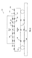
- FIG. 2 shows a cross-sectional diagram of an IC device 200 coupled to a printed circuit board (PCB) 250, according to an embodiment of the present invention.
- IC device 200 includes an IC die 202 coupled to a substrate 204 through an adhesive 206.
- IC die 202 has a first plurality of wirelessly enabled functional blocks 220 and contact pads 207 formed on a surface 208.
- Substrate 204 has a second and third pluralities of wirelessly enabled functional blocks 230 and 240 formed on surfaces 210 and 212, respectively.
- Substrate 204 also has solder bumps 209 and solder balls 211 formed on surfaces 210 and 212, respectively.
- PCB 250 has a fourth plurality of wirelessly enabled functional blocks 260 and solder balls 218 formed thereon.
- First and second ground rings 214 and 216 are formed on surface 210 of substrate 204.
- Adhesive 206 attaches IC die 202 to substrate 204.
- adhesive 206 is an electrically non-conductive epoxy.
- IC die 202 is both ohmically and wirelessly coupled to substrate 204.
- contact pads 207 of IC die 202 are physically coupled to solder bumps 209 of substrate 204.
- ones of first plurality of wirelessly enabled functional blocks 220 are configured to wirelessly communicate with respective ones of second plurality of wirelessly enabled functional blocks 230.
- substrate 204 is both ohmically and wirelessly coupled to PCB 250.
- surface 212 of substrate 204 is physically connected to solder balls 218 through which substrate 204 is coupled to PCB 250.
- ones of third plurality of wirelessly enabled functional blocks 240 are configured to wirelessly communicate with respective ones of fourth plurality of wirelessly enabled functional blocks 260 located on PCB 250.
- multiple access techniques such as FDMA, TDMA, or CDMA can be used by the wirelessly enabled functional blocks so that different ones of first, second, third, and fourth pluralities of wirelessly enabled functional blocks 220, 230, 240, and 260 do not interfere with each other.
- the structure of first, second, third, and fourth pluralities of wirelessly enabled functional blocks 220, 230, 240, and 260 will be described in greater detail with respect to FIG. 3 below.
- communications between first, second, third, and fourth pluralities of wirelessly enabled functional blocks 220, 230, 240, and 260 are susceptible to electromagnetic interference originating outside of IC device 200.
- the communications between first, second, third, and fourth pluralities of wirelessly enabled functional blocks 220, 230, 240, and 260 are especially susceptible to interference because these communications occur wirelessly. As such, electromagnetic interference can seriously jeopardize the fidelity of the communications between the different pluralities of wirelessly enabled functional blocks.
- ground rings 214 and 216 are provided in IC device 200, shown in FIG. 2 .
- Ground rings 214 and 216 can be formed as metal traces on surface 210 of substrate 204 and can be coupled to ground potential through substrate 204, e.g., through a ground plane of substrate 204.
- ground rings 214 and 216 can be formed out of conductive metals such as copper, gold, a through substrate 204, e.g., through a ground plane of substrate 204.
- ground rings 214 and 216 can be formed out of conductive metals such as copper, gold, a nickel-gold alloy, silver, or other metal.
- ground rings 214 and 216 act as Faraday cages that prevent electromagnetic waves from entering the spaces between one or more of first, second, third, and fourth pluralities of wirelessly enabled functional blocks 220, 230, 240, and 260.
- ground rings 214 and 216 can also be used as a common ground for the components of IC device 200.
- ground rings 214 and 216 can be used as a common ground for ones of first, second, third, and fourth pluralities of wirelessly enabled functional blocks 220, 230, 240, and 260.
- ground rings 214 and 216 can be configured to be flexible.
- ground rings 214 and 216 can be formed to be relatively thin, e.g., about the same or less than the thickness of typical traces formed on substrate 204 and can be made out of flexible or malleable materials, such as a metal. In doing so, ground rings 214 and 216 do not exert additional stress on substrate 204 when IC device 200 is bent or otherwise stressed, thus reducing the likelihood that substrate 204 will break or otherwise be damaged.
- IC device 200 includes two ground rings, namely ground rings 214 and 216. As would be apparent to those skilled in the relevant arts based on the description herein, IC device 200 can include any number of ground rings similar to ground rings 214 and 216 (e.g., one, three, or more than three) without departing from the scope of the present invention.
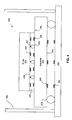
- FIG. 3 shows diagram of a wirelessly enabled functional block 300, according to an embodiment of the present invention.
- Wirelessly enabled functional block 300 includes an antenna 302 and vias 304a and 304b (collectively "304"), which feed antenna 302.
- first, second, third, and fourth pluralities of wirelessly enabled functional blocks 220, 230, 240, and 260 can be implemented in a manner substantially similar to wirelessly enabled functional block 300.
- at least one of vias 304 is a through silicon via (e.g., in the embodiment in which wirelessly enabled functional block 300 is formed on surface 208 of IC die 202).
- antenna 302 is a dipole antenna.
- antenna 302 can be formed out of metal traces or planes.
- dipole antenna 302 can be formed using embodiments, antenna 302 can be another type of antenna.
- antenna 302 can be a patch antenna having a square or rectangular shape.
- Vias 304 can be used to drive antenna with or received from antenna a single ended signal or a differential signal.
- via 304a can be coupled to a signal plane (e.g., a ground plane through one or more of ground rings 214 and 216) and via 304b can be coupled to a circuit block or other element that provides a single-ended signal.
- each of vias 304 can be coupled to circuit blocks or other elements that provide components of a differential signal.
- wirelessly enabled functional block 300 optionally includes a transceiver 306.
- antenna 302 is fed by transceiver 306.
- Transceiver 306 can be coupled to a signal plane using vias of a die, a substrate, or a PCB.
- transceiver 306 is also coupled to a circuit block or a portion of a PCB (e.g., through a substrate).
- Transceiver 306 can be configured to transmit signals received from the circuit block or the PCB and/or convey received signals to the circuit block or the PCB.
- transceiver 306 can have additional functionality.
- transceiver 306 may be capable of performing signal processing tasks such as modulation and demodulation and to allow for the use of the multiple access noted above.
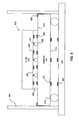
- FIG. 4 shows a cross-sectional diagram of an IC device 400 coupled to PCB 250, according to an embodiment of the present invention.
- IC device 400 is substantially similar to IC device 200, except that IC device 400 does not include ground rings 214 and 216. Instead, a ground ring 402 is provided on PCB 250.
- Ground ring 402 like ground rings 214 and 216, can maintain a ground potential and thereby operate as a Faraday cage, thereby providing electromagnetic shielding.
- ground ring 402 provides substantial electromagnetic shielding for third and fourth pluralities of wirelessly enabled functional blocks 240 and 260, as well as for first and second pluralities of wirelessly enabled functional blocks 220 and 230.
- ground ring 402 can acquire ground potential through one or more traces formed on PCB 250 (not shown).
- ground ring 402 is physically separated from substrate 204. As such, ground ring 402 does not exert additional stresses on substrate 204 when substrate 204 is bent or otherwise stressed. In an embodiment, ground ring 402 can be
- ground ring 402 is physically separated from substrate 204. As such, ground ring 402 does not exert additional stresses on substrate 204 when substrate 204 is bent or otherwise stressed.
- ground ring 402 can be formed out of flexible materials to prevent cracking or damage to ground ring 402 when stresses are imposed.
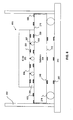
- FIG. 5 shows a cross-sectional diagram of an IC device 500 coupled to PCB 250, according to an embodiment of the present invention.
- IC device 500 is substantially similar to IC device 400, except that IC device 500 additionally includes a coupling member 502.
- Coupling member 502 couples substrate 204 to ground ring 402.
- coupling member 502 can be formed out of an electrically conductive material, e.g., copper.
- coupling member 502 electrically couples ground ring 402 to substrate 204.
- ground ring 402 can acquire a ground potential from substrate 204.
- coupling member 502 can be configured so as to allow for independent movement of substrate 204 and ground ring 402.
- coupling member 502 can be formed out of a metal or other material that allows substrate 204 to slide with respect to ground ring 402.
- ground ring 402 can be made out of a flexible or malleable material to further reduce any stress it would impose on substrate 204.
- FIG. 6 shows a cross-sectional diagram of an IC device 600 coupled to PCB 250, according to an embodiment of the present invention.
- IC device 600 is substantially similar to IC device 500, except that IC device 600 additionally includes a second ground ring 602.
- Second ground 602 can be substantially similar to ground rings 214 and 216, described with reference to FIG. 2 .
- Second ground ring 602 can provide additional shielding from electromagnetic interference.
- IC device 600 can include any number of ground rings similar to ground ring 602 without departing from the scope of the present invention.
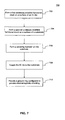
- FIG. 7 shows a flowchart 700 providing example steps for assembling an IC device, according to an embodiment of the present invention.
- FIG. 7 shows a flowchart 700 providing example steps for assembling an IC device, according to an embodiment of the present invention.
- Other structural and operational embodiments will be apparent to persons skilled in the relevant art(s) based on
- a first plurality of wirelessly enabled functional block is formed on a surface of an IC die.
- first wirelessly enabled functional blocks 220 can be formed on surface 208 of IC die 202.
- a second wirelessly enabled functional block is formed on a surface of a substrate.
- second plurality of wirelessly enabled functional blocks 230 can be formed on surface 210 of substrate 204.
- a third wirelessly enabled functional block can be formed on another surface of the substrate.
- third plurality of wirelessly enabled functional blocks 240 can be formed on surface 212 of substrate 204.
- one or more of the first, second, and third wirelessly enabled functional blocks can be formed a combination of traces and vias as described with reference to FIG. 3 , above. Additional functionality can be provided by, for example, coupling the traces to a transceiver to form a wirelessly enabled functional block capable of performing signal processing among other tasks.
- a coupling member is formed on the substrate.
- coupling member 502 can be formed on substrate 204.
- Coupling member 502 can be configured to couple substrate 204 to ground ring 402.
- coupling member 502 can be configured to allow substrate 204 to move independently of ground ring 402 by allowing substrate 204 to slide relative to ground ring 402.
- step 708 the IC die is coupled to the substrate.
- IC die 202 is coupled to substrate 204 using adhesive 206.
- a ground ring configured to provide electromagnetic shielding is provided.
- ground rings 214 and 216 are provided on substrate 204.
- ground ring 402 is provided on PCB 250.
- ground rings 214, 216, and 402 are configured to provide electromagnetic shielding for ones of first, second, third, and fourth pluralities of wirelessly enabled functional blocks 220, 230, 240, and 260.
Landscapes
- Engineering & Computer Science (AREA)
- Microelectronics & Electronic Packaging (AREA)
- Shielding Devices Or Components To Electric Or Magnetic Fields (AREA)
- Near-Field Transmission Systems (AREA)
- Physics & Mathematics (AREA)
- Health & Medical Sciences (AREA)
- Electromagnetism (AREA)
- Toxicology (AREA)
- Semiconductor Integrated Circuits (AREA)
Description
- The present invention generally relates to integrated circuit (IC) devices, and more particularly to communications involving IC devices.
- Integrated circuit (IC) devices typically include an IC die housed in a package. The IC device can be coupled to a printed circuit board (PCB) to enable communication between the IC device and other devices coupled to the PCB. For example, in array-type packages, an IC die is often coupled to a substrate, which is coupled to an array of connection elements, e.g., an array of solder balls. The array of connections elements is then physically coupled to the PCB.
- An IC die can be coupled to a substrate in a variety of ways. For example, in die-down flip-chip packages, solder bumps can be used to couple contact pads on a surface of the IC die to contact pads located on the substrate. In another example, wirebonds can be used to couple bond pads on a surface of the IC die to bond fingers located on the substrate.
- Conventional ways of coupling an IC die to a substrate can, however, be costly. For example, the materials used to create wirebonds, e.g., gold, can be expensive, thus increasing the cost of the entire device. Furthermore, the conventional ways of coupling the IC die to the substrate can also be susceptible to manufacturing defects. For example, wirebonds and/or solder bumps can break or be damaged during the manufacturing and assembly processes, reducing the throughput for the IC device.
- Furthermore, conventional ways of coupling different IC devices can also have drawbacks. For example, when IC devices are coupled together using a PCB, the elements used to couple the IC devices to the PCB can break or be damaged during manufacturing or field application. Additionally, almost all communications within an IC device or between the IC device and other devices (e.g., through a PCB) are susceptible to electromagnetic interference. The presence of this interference can compromise the fidelity of communications, and thus significantly hamper the performance of the overall system.
-
US 2009/0266900 A1 discloses a wireless IC device with a wireless IC that processes transmission and reception signals, wherein a feeder circuit incorporates an inductance element connected to the wireless IC in a galvanically conductive state and in which a feeder electrode coupled to the inductance element is provided on a surface of the substrate or an inside of the substrate, and a radiation plate is electromagnetically coupled to the feeder electrode. - According to an aspect of the present invention, an integrated circuit (IC) device is provided according to the attached independent claim 1.
- Advantageously, the ground ring comprises a metal trace formed on the surface of the substrate.
- Advantageously, the IC device further comprises:
- a second ground ring formed on the surface of the substrate, wherein the second ground ring comprises a second trace formed on the surface of the substrate.
- Advantageously, the IC device is configured to be coupled to a printed circuit board (PCB) and wherein the ground ring is coupled to the PCB.
- Advantageously, the ground ring comprises a flexible material.
- Advantageously, the IC device further comprises a coupling member configured to couple the ground ring to the substrate.
- Advantageously, the coupling member is configured to allow for the substrate to move independently of the ground ring.
- Advantageously, the IC device further comprises a second ground ring located on the surface of the substrate.
- Advantageously, the IC device is configured to be coupled to a surface of a printed circuit board (PCB), the IC device further comprising:
- a third wirelessly enabled functional block located on a second surface of the substrate, the second surface of the substrate opposing the first surface of the substrate, wherein the third wirelessly enabled functional block is configured to wirelessly communicate with a fourth wirelessly enabled functional block located on the surface of the PCB.
- Advantageously, the ground ring is configured to provide electromagnetic shielding for the third and fourth wirelessly enabled functional blocks.
- Advantageously, the IC device further comprises a solder ball coupled to the second surface of the substrate that is configured to be coupled to the surface of the PCB.
- According to another aspectof the present invention, a method of assembling an integrated circuit (IC) device is provided according to the attached independent claim 15.
- Advantageously, the method further comprises:
- forming a metal trace on the surface of the substrate.
- Advantageously, the method further comprises:
- providing a second ground ring configured to provide electromagnetic shielding for the first and second wirelessly enabled functional blocks.
- The accompanying drawings, which are incorporated herein and form a part of the specification, illustrate the present invention and, together with the description, further serve to explain the principles of the invention and to enable a person skilled in the pertinent art to make and use the invention.
-
FIG. 1 is a cross-sectional view of a conventional die down ball grid array package. -
FIGS. 2 is a cross-sectional view of an IC device having a ground ring located on a substrate, according to an embodiment of the present invention. -
FIG. 3 is a diagram of a wirelessly enabled functional block, according to an embodiment of the invention. -
FIGS. 4-6 are cross-sectional diagrams of IC devices having a ground ring coupled to a printed circuit board, according to embodiments of the present invention. -
FIG. 7 is a flowchart of example steps for assembling an IC device, according to embodiments of the invention. - The present invention will now be described with reference to the accompanying drawings. In the drawings, like reference numbers indicate identical or functionally similar elements. Additionally, the left-most digit(s) of a reference number identifies the drawing in which the reference number first appears.
- References in the specification to "one embodiment", "an embodiment", "an example embodiment", etc., indicate that the embodiment described may include a particular feature, structure, or characteristic, but every embodiment may not necessarily include the particular feature, structure, or characteristic. Moreover, such phrases are not necessarily referring to the same embodiment. Further, when a particular feature, structure, or characteristic is described in connection with an embodiment, it is submitted that it is within the knowledge of one skilled in the art to effect such feature, structure, or characteristic in connection with other embodiments whether or not explicitly described.
- Furthermore, it should be understood that spatial descriptions (e.g., "above", "below", "left," "right," "up", "down", "top", "bottom", etc.) used herein are for purposes of illustration only, and that practical implementations of the structures described herein can be spatially arranged in any orientation or manner.
-
FIG. 1 shows a cross-sectional view of a conventional die down ball grid array (BGA)package 100. BGApackage 100 includes an IC die 110 coupled to atop surface 125 of asubstrate 120 viasolder bumps 130. BGApackage 100 is a die down package in which anactive surface 115 of die 110faces substrate 120. On the other hand, in die up packages, the active surface of the die faces away from the substrate. -
Active surface 115 often includes power and ground distribution rails and input/output contact pads. A plurality ofsolder bumps 130 can be distributed acrossactive surface 115 of flip chip die 110 to respectively connect flip chip die 110 tosubstrate 120. As shown inFIG. 1 , asolder mask 190 surrounds the area wheresolder bumps 130 are located. - In the conventional arrangement shown in
FIG. 1 ,vias 140 connectsolder bumps 130, traces, and/or viapads 150 attop surface 125 ofsubstrate 120 tosolder balls 180 at a bottom surface ofsubstrate 120. As shown inFIG. 1 ,substrate 120 can includebump pads 160 andball pads 170.Bump pads 160 are connected tosolder bumps 130 attop surface 125 ofsubstrate 120.Ball pads 170 are connected tosolder balls 180 at the bottom surface ofsubstrate 120.Solder balls 180 can electrically connect flipchip BGA package 100 to any suitable surface having electrically conductive connections, such as a PCB. - In embodiments described herein, IC devices are provided that include wirelessly enabled functional blocks. The wirelessly enabled functional blocks can be used to communicate signals between an IC die and a substrate. Additionally or alternatively, wirelessly enabled functional blocks can be used to communicate signals between the substrate and a printed circuit board (PCB). In an embodiment, a ground ring can also be provided that provides electromagnetic shielding for the wirelessly enabled functional blocks. Because the wireless communications between wirelessly enabled functional blocks are especially susceptible to electromagnetic interference, the ground ring providing for fidelity of communication between the wirelessly enabled functional blocks can be especially useful.
-
FIG. 2 shows a cross-sectional diagram of anIC device 200 coupled to a printed circuit board (PCB) 250, according to an embodiment of the present invention.IC device 200 includes an IC die 202 coupled to asubstrate 204 through an adhesive 206. IC die 202 has a first plurality of wirelessly enabledfunctional blocks 220 andcontact pads 207 formed on asurface 208.Substrate 204 has a second and third pluralities of wirelessly enabledfunctional blocks surfaces Substrate 204 also hassolder bumps 209 and solder balls 211 formed onsurfaces PCB 250 has a fourth plurality of wirelessly enabledfunctional blocks 260 andsolder balls 218 formed thereon. First and second ground rings 214 and 216 are formed onsurface 210 ofsubstrate 204. -
Adhesive 206 attaches IC die 202 tosubstrate 204. In an embodiment, adhesive 206 is an electrically non-conductive epoxy. - As shown in
FIG. 2 , IC die 202 is both ohmically and wirelessly coupled tosubstrate 204. In particular,contact pads 207 of IC die 202 are physically coupled tosolder bumps 209 ofsubstrate 204. Moreover, ones of first plurality of wirelessly enabledfunctional blocks 220 are configured to wirelessly communicate with respective ones of second plurality of wirelessly enabled functional blocks 230. Similarly,substrate 204 is both ohmically and wirelessly coupled toPCB 250. In particular,surface 212 ofsubstrate 204 is physically connected tosolder balls 218 through whichsubstrate 204 is coupled toPCB 250. Additionally, ones of third plurality of wirelessly enabledfunctional blocks 240 are configured to wirelessly communicate with respective ones of fourth plurality of wirelessly enabledfunctional blocks 260 located onPCB 250. In an embodiment, multiple access techniques such as FDMA, TDMA, or CDMA can be used by the wirelessly enabled functional blocks so that different ones of first, second, third, and fourth pluralities of wirelessly enabledfunctional blocks functional blocks FIG. 3 below. - Like all communications between IC die 202,
substrate 204, andPCB 250, communications between first, second, third, and fourth pluralities of wirelessly enabledfunctional blocks IC device 200. The communications between first, second, third, and fourth pluralities of wirelessly enabledfunctional blocks - To reduce the electromagnetic interference, ground rings 214 and 216 are provided in
IC device 200, shown inFIG. 2 . Ground rings 214 and 216 can be formed as metal traces onsurface 210 ofsubstrate 204 and can be coupled to ground potential throughsubstrate 204, e.g., through a ground plane ofsubstrate 204. In an embodiment, ground rings 214 and 216 can be formed out of conductive metals such as copper, gold, a throughsubstrate 204, e.g., through a ground plane ofsubstrate 204. In an embodiment, ground rings 214 and 216 can be formed out of conductive metals such as copper, gold, a nickel-gold alloy, silver, or other metal. In operation, ground rings 214 and 216 act as Faraday cages that prevent electromagnetic waves from entering the spaces between one or more of first, second, third, and fourth pluralities of wirelessly enabledfunctional blocks IC device 200. For example, ground rings 214 and 216 can be used as a common ground for ones of first, second, third, and fourth pluralities of wirelessly enabledfunctional blocks - In an embodiment, ground rings 214 and 216 can be configured to be flexible. For example, ground rings 214 and 216 can be formed to be relatively thin, e.g., about the same or less than the thickness of typical traces formed on
substrate 204 and can be made out of flexible or malleable materials, such as a metal. In doing so, ground rings 214 and 216 do not exert additional stress onsubstrate 204 whenIC device 200 is bent or otherwise stressed, thus reducing the likelihood thatsubstrate 204 will break or otherwise be damaged. - As shown in
FIG. 2 ,IC device 200 includes two ground rings, namely ground rings 214 and 216. As would be apparent to those skilled in the relevant arts based on the description herein,IC device 200 can include any number of ground rings similar to ground rings 214 and 216 (e.g., one, three, or more than three) without departing from the scope of the present invention. -
FIG. 3 shows diagram of a wirelessly enabledfunctional block 300, according to an embodiment of the present invention. Wirelessly enabledfunctional block 300 includes anantenna 302 andvias antenna 302. One or more of first, second, third, and fourth pluralities of wirelessly enabledfunctional blocks functional block 300. In an embodiment, at least one of vias 304 is a through silicon via (e.g., in the embodiment in which wirelessly enabledfunctional block 300 is formed onsurface 208 of IC die 202). - As shown in
FIG. 3 ,antenna 302 is a dipole antenna. Other antenna configurations can be used as appropriate. In an embodiment,antenna 302 can be formed out of metal traces or planes. For example,dipole antenna 302 can be formed using embodiments,antenna 302 can be another type of antenna. For example,antenna 302 can be a patch antenna having a square or rectangular shape. - Vias 304 can be used to drive antenna with or received from antenna a single ended signal or a differential signal. For example, via 304a can be coupled to a signal plane (e.g., a ground plane through one or more of ground rings 214 and 216) and via 304b can be coupled to a circuit block or other element that provides a single-ended signal. Alternatively, each of vias 304 can be coupled to circuit blocks or other elements that provide components of a differential signal.
- As shown in
FIG. 3 , wirelessly enabledfunctional block 300 optionally includes atransceiver 306. In such an embodiment,antenna 302 is fed bytransceiver 306.Transceiver 306 can be coupled to a signal plane using vias of a die, a substrate, or a PCB. In an embodiment,transceiver 306 is also coupled to a circuit block or a portion of a PCB (e.g., through a substrate).Transceiver 306 can be configured to transmit signals received from the circuit block or the PCB and/or convey received signals to the circuit block or the PCB. In a further embodiment,transceiver 306 can have additional functionality. For example,transceiver 306 may be capable of performing signal processing tasks such as modulation and demodulation and to allow for the use of the multiple access noted above. -
FIG. 4 shows a cross-sectional diagram of anIC device 400 coupled toPCB 250, according to an embodiment of the present invention.IC device 400 is substantially similar toIC device 200, except thatIC device 400 does not include ground rings 214 and 216. Instead, aground ring 402 is provided onPCB 250.Ground ring 402, like ground rings 214 and 216, can maintain a ground potential and thereby operate as a Faraday cage, thereby providing electromagnetic shielding. Unlike ground rings 214 and 216, however,ground ring 402 provides substantial electromagnetic shielding for third and fourth pluralities of wirelessly enabledfunctional blocks functional blocks ground ring 402 can acquire ground potential through one or more traces formed on PCB 250 (not shown). - As shown in
FIG. 4 ,ground ring 402 is physically separated fromsubstrate 204. As such,ground ring 402 does not exert additional stresses onsubstrate 204 whensubstrate 204 is bent or otherwise stressed. In an embodiment,ground ring 402 can be - As shown in
FIG. 4 ,ground ring 402 is physically separated fromsubstrate 204. As such,ground ring 402 does not exert additional stresses onsubstrate 204 whensubstrate 204 is bent or otherwise stressed. In an embodiment,ground ring 402 can be formed out of flexible materials to prevent cracking or damage toground ring 402 when stresses are imposed. -
FIG. 5 shows a cross-sectional diagram of anIC device 500 coupled toPCB 250, according to an embodiment of the present invention.IC device 500 is substantially similar toIC device 400, except thatIC device 500 additionally includes acoupling member 502. Couplingmember 502couples substrate 204 toground ring 402. In an embodiment,coupling member 502 can be formed out of an electrically conductive material, e.g., copper. In a further embodiment,coupling member 502 electrically couplesground ring 402 tosubstrate 204. Thus,ground ring 402 can acquire a ground potential fromsubstrate 204. - Moreover,
coupling member 502 can be configured so as to allow for independent movement ofsubstrate 204 andground ring 402. For example,coupling member 502 can be formed out of a metal or other material that allowssubstrate 204 to slide with respect toground ring 402. Thus, whenIC device 500 is bent or otherwise stressed,coupling member 502 can be used ensure thatground ring 402 does not impose additional stresses onsubstrate 204. In a further embodiment,ground ring 402 can be made out of a flexible or malleable material to further reduce any stress it would impose onsubstrate 204. -
FIG. 6 shows a cross-sectional diagram of anIC device 600 coupled toPCB 250, according to an embodiment of the present invention.IC device 600 is substantially similar toIC device 500, except thatIC device 600 additionally includes asecond ground ring 602.Second ground 602 can be substantially similar to ground rings 214 and 216, described with reference toFIG. 2 .Second ground ring 602 can provide additional shielding from electromagnetic interference. As would apparent to those skilled in the relevant arts,IC device 600 can include any number of ground rings similar toground ring 602 without departing from the scope of the present invention. -
FIG. 7 shows aflowchart 700 providing example steps for assembling an IC device, according to an embodiment of the present invention. Other structural and operational embodiments will be apparent to persons skilled in the relevant art(s) based - In
step 702, a first plurality of wirelessly enabled functional block is formed on a surface of an IC die. For example, inFIG. 2 , first wirelessly enabledfunctional blocks 220 can be formed onsurface 208 of IC die 202. - In
step 704, a second wirelessly enabled functional block is formed on a surface of a substrate. For example, inFIG. 2 , second plurality of wirelessly enabledfunctional blocks 230 can be formed onsurface 210 ofsubstrate 204. In a further embodiment, a third wirelessly enabled functional block can be formed on another surface of the substrate. For example, inFIG. 2 , third plurality of wirelessly enabledfunctional blocks 240 can be formed onsurface 212 ofsubstrate 204. In an embodiment, one or more of the first, second, and third wirelessly enabled functional blocks can be formed a combination of traces and vias as described with reference toFIG. 3 , above. Additional functionality can be provided by, for example, coupling the traces to a transceiver to form a wirelessly enabled functional block capable of performing signal processing among other tasks. - In
optional step 706, a coupling member is formed on the substrate. For example, inFIG. 5 ,coupling member 502 can be formed onsubstrate 204. Couplingmember 502 can be configured to couplesubstrate 204 toground ring 402. In a further embodiment,coupling member 502 can be configured to allowsubstrate 204 to move independently ofground ring 402 by allowingsubstrate 204 to slide relative toground ring 402. - In
step 708, the IC die is coupled to the substrate. For example, inFIG. 2 , IC die 202 is coupled tosubstrate 204 using adhesive 206. - In
step 710, a ground ring configured to provide electromagnetic shielding is provided. For example, inFIG. 2 , ground rings 214 and 216 are provided onsubstrate 204. In another embodiment, inFIG. 3 ,ground ring 402 is provided onPCB 250. As described above, ground rings 214, 216, and 402 are configured to provide electromagnetic shielding for ones of first, second, third, and fourth pluralities of wirelessly enabledfunctional blocks - The embodiments of the invention have been described above with the aid of functional building blocks illustrating the implementation of specified functions and relationships thereof. The boundaries of these functional building blocks have been arbitrarily defined herein for the convenience of the description. Alternate boundaries can be defined so long as the specified functions and relationships thereof are appropriately performed and fall within the scope of the present invention.
- The foregoing description of the specific embodiments will so fully reveal the general nature of the invention that others can, by applying knowledge within the skill of the art, adapt for various applications such specific embodiments, without undue experimentation, without departing from the general scope of the present invention. It is to be understood that the phraseology or terminology herein is for the purpose of description and not of limitation, such that the terminology or phraseology of the present specification is to be interpreted by the skilled artisan in light of the teachings and guidance.
- The breadth and scope of the present invention should not be limited by any of the above-described exemplary embodiments, but should be defined only in accordance with the following claims.
Claims (15)
- An integrated circuit (IC) device, comprising:a substrate (204);an IC die (202) coupled to a surface (210) of the substrate (204);a first wirelessly enabled functional block (220) located on the IC die (202), wherein the first wirelessly enabled functional block (220) is configured to wirelessly communicate with a second wirelessly enabled functional block (230) located on the substrate (204);a ground ring (214, 216, 402, 602) configured to provide electromagnetic shielding for the first and second wirelessly enabled functional blocks (220, 230), characterized in that the ground ring (214, 216, 602) is located on the surface (210) of the substrate (204) and/or the ground ring (402) is provided on the surface of the PCB (250).
- The IC device of claim 12, wherein the ground ring (214, 216, 402, 602) comprises a metal trace formed on the surface (210) of the substrate (204).
- The IC device of claim 3, wherein the ground ring (602) located on the surface (210) of the substrate (204) comprises a second trace formed on the surface (210) of the substrate (204).
- The IC device of claim 1, wherein the IC device is configured to be coupled to a printed circuit board, PCB, (250), the ground ring (402) is provided on the PCB (250), and coupled to the substrate (204).
- The IC device of claim 4, wherein the ground ring (214, 216, 402, 602) comprises a flexible material.
- The IC device of claim 4, further comprising a coupling member (502) configured to couple the ground ring (402) to the substrate (204).
- The IC device of claim 6, wherein the coupling member (502) is configured to allow for the substrate (204) to move independently of the ground ring (402) by allowing substrate (204) to slide relative to ground ring (402).
- The IC device of claim 1, wherein the IC device is configured to be coupled to a surface of a printed circuit board, PCB, (250), the IC device further comprising:a third wirelessly enabled functional block (240) located on a second surface (210) of the substrate (204), the second surface (212) of the substrate (204) opposing the first surface (210) of the substrate (204), wherein the third wirelessly enabled functional block (240) is configured to wirelessly communicate with a fourth wirelessly enabled functional block (260) located on the surface of the PCB (250).
- The IC device of claim 8, wherein the ground ring (214, 216) located on the surface (210) of the substrate (204) is configured to provide electromagnetic shielding for the third and fourth wirelessly enabled functional blocks (240, 260), and the ground ring (402) provided on the surface of the PCB (250) is configured to provide electromagnetic shielding for the first and second wirelessly enabled functional blocks (220, 230).
- The IC device of claim 8, further comprising a solder ball coupled to the second surface (212) of the substrate (204) that is configured to be coupled to the surface of the PCB (250).
- The IC device of claim 1, wherein each of the first plurality of wirelessly enabled functional blocks (220) is configured to wirelessly communicate with a respective one of a second plurality of wirelessly enabled functional blocks (230) located on the substrate (204).
- The IC device of claim 1, wherein each of the first plurality of wirelessly enabled functional blocks (220) is configured to use a multiple access technique so that different ones of first, second, third, and fourth pluralities of wirelessly enabled functional blocks (220, 230, 240, 260) do not interfere with each other.
- The IC device of claim 1, wherein the first wirelessly enabled functional block (220) comprises an antenna (302).
- The IC device of claim 1, wherein the first wirelessly enabled functional block (220) further comprises a transceiver (306).
- A method of assembling an integrated circuit (IC) device, comprising:forming a first wirelessly enabled functional block (220) on a surface (208) of an IC die (202);forming a second wirelessly enabled functional block (230) on a surface (210) of the substrate (204), wherein the second wirelessly enabled functional block (230) is configured to wirelessly communicate with the first wirelessly enabled functional block (220);coupling the IC die (202) to the substrate (204);providing a ground ring (214, 216, 402, 602) configured to provide electromagnetic shielding for the first and second wirelessly enabled functional blocks (220, 230) wherein the ground ring (214, 216, 602) is located on the surface (210) of the substrate (204) and/or the ground ring (402) is provided on the surface of the PCB (250).
Applications Claiming Priority (1)
| Application Number | Priority Date | Filing Date | Title |
|---|---|---|---|
| US13/249,885 US8928139B2 (en) | 2011-09-30 | 2011-09-30 | Device having wirelessly enabled functional blocks |
Publications (2)
| Publication Number | Publication Date |
|---|---|
| EP2575416A1 EP2575416A1 (en) | 2013-04-03 |
| EP2575416B1 true EP2575416B1 (en) | 2014-12-10 |
Family
ID=46796217
Family Applications (1)
| Application Number | Title | Priority Date | Filing Date |
|---|---|---|---|
| EP12005675.9A Active EP2575416B1 (en) | 2011-09-30 | 2012-08-03 | A device having wirelessly enabled functional blocks |
Country Status (5)
| Country | Link |
|---|---|
| US (1) | US8928139B2 (en) |
| EP (1) | EP2575416B1 (en) |
| KR (1) | KR101425460B1 (en) |
| CN (2) | CN103035628B (en) |
| TW (1) | TWI566371B (en) |
Families Citing this family (6)
| Publication number | Priority date | Publication date | Assignee | Title |
|---|---|---|---|---|
| US8901945B2 (en) | 2011-02-23 | 2014-12-02 | Broadcom Corporation | Test board for use with devices having wirelessly enabled functional blocks and method of using same |
| US8928139B2 (en) * | 2011-09-30 | 2015-01-06 | Broadcom Corporation | Device having wirelessly enabled functional blocks |
| CN214960295U (en) * | 2018-08-22 | 2021-11-30 | 株式会社村田制作所 | Transmission line substrate and connection structure of transmission line substrate |
| US11088108B2 (en) * | 2019-06-27 | 2021-08-10 | Taiwan Semiconductor Manufacturing Co., Ltd. | Chip package structure including ring-like structure and method for forming the same |
| US11791535B2 (en) | 2020-09-28 | 2023-10-17 | Samsung Electronics Co., Ltd. | Non-galvanic interconnect for planar RF devices |
| EP4293817A1 (en) * | 2022-06-13 | 2023-12-20 | Nxp B.V. | Rf package and method of manufacture of an rf package |
Family Cites Families (59)
| Publication number | Priority date | Publication date | Assignee | Title |
|---|---|---|---|---|
| US6728113B1 (en) * | 1993-06-24 | 2004-04-27 | Polychip, Inc. | Method and apparatus for non-conductively interconnecting integrated circuits |
| FR2727227B1 (en) | 1994-11-17 | 1996-12-20 | Schlumberger Ind Sa | ACTIVE SECURITY DEVICE WITH ELECTRONIC MEMORY |
| JP3378435B2 (en) | 1995-09-29 | 2003-02-17 | 株式会社東芝 | Ultra-high frequency band wireless communication device |
| FR2765399B1 (en) | 1997-06-27 | 2001-12-07 | Sgs Thomson Microelectronics | SEMICONDUCTOR DEVICE WITH REMOTE EXCHANGES |
| FR2769110B1 (en) | 1997-09-26 | 1999-12-03 | Gemplus Card Int | METHOD FOR MANUFACTURING AN ELECTRONIC MODULE OR LABEL, MODULE OR LABEL OBTAINED AND SUPPORT COMPRISING SUCH A MODULE OR LABEL |
| EP0932200A3 (en) | 1998-01-22 | 2000-08-23 | International Business Machines Corporation | Heat sink device for microprocessor |
| EP0978729A3 (en) | 1998-08-07 | 2002-03-20 | Hitachi, Ltd. | High-frequency transmitter-receiving apparatus for such an application as vehicle-onboard radar system |
| US6542720B1 (en) | 1999-03-01 | 2003-04-01 | Micron Technology, Inc. | Microelectronic devices, methods of operating microelectronic devices, and methods of providing microelectronic devices |
| JP3675688B2 (en) | 2000-01-27 | 2005-07-27 | 寛治 大塚 | Wiring board and manufacturing method thereof |
| EP1126522A1 (en) * | 2000-02-18 | 2001-08-22 | Alcatel | Packaged integrated circuit with radio frequency antenna |
| JP4848108B2 (en) | 2001-09-14 | 2011-12-28 | インターナショナル・ビジネス・マシーンズ・コーポレーション | Data processing system |
| US6885090B2 (en) | 2001-11-28 | 2005-04-26 | North Carolina State University | Inductively coupled electrical connectors |
| US6670692B1 (en) | 2002-10-09 | 2003-12-30 | Silicon Integrated Systems Corp. | Semiconductor chip with partially embedded decoupling capacitors |
| US7095620B2 (en) | 2002-11-27 | 2006-08-22 | International Business Machines Corp. | Optically connectable circuit board with optical component(s) mounted thereon |
| US20050075080A1 (en) | 2003-10-03 | 2005-04-07 | Nanyang Technological University | Inter-chip and intra-chip wireless communications systems |
| US20050225481A1 (en) | 2004-04-12 | 2005-10-13 | Bonthron Andrew J | Method and apparatus for automotive radar sensor |
| US7525199B1 (en) | 2004-05-21 | 2009-04-28 | Sun Microsystems, Inc | Packaging for proximity communication positioned integrated circuits |
| DE102004059333A1 (en) | 2004-12-09 | 2006-06-14 | Robert Bosch Gmbh | Antenna arrangement for a radar transceiver |
| DE102004063541A1 (en) | 2004-12-30 | 2006-07-13 | Robert Bosch Gmbh | Antenna arrangement for a radar transceiver |
| US7502965B2 (en) | 2005-02-07 | 2009-03-10 | Broadcom Corporation | Computer chip set having on board wireless interfaces to support test operations |
| US7479841B2 (en) | 2005-02-15 | 2009-01-20 | Northrop Grumman Corporation | Transmission line to waveguide interconnect and method of forming same including a heat spreader |
| US20060285480A1 (en) | 2005-06-21 | 2006-12-21 | Janofsky Eric B | Wireless local area network communications module and integrated chip package |
| US20090000815A1 (en) * | 2007-06-27 | 2009-01-01 | Rf Micro Devices, Inc. | Conformal shielding employing segment buildup |
| US20070065984A1 (en) | 2005-09-22 | 2007-03-22 | Lau Daniel K | Thermal enhanced package for block mold assembly |
| US7405477B1 (en) * | 2005-12-01 | 2008-07-29 | Altera Corporation | Ball grid array package-to-board interconnect co-design apparatus |
| EP1967876A4 (en) | 2005-12-27 | 2013-04-17 | Ibiden Co Ltd | Optical and electrical composite wiring board and method for fabricating same |
| WO2007101345A1 (en) | 2006-03-07 | 2007-09-13 | Scanimetrics Inc. | Method and apparatus for interrogating an electronic component |
| US7692295B2 (en) | 2006-03-31 | 2010-04-06 | Intel Corporation | Single package wireless communication device |
| EP2830006A1 (en) * | 2006-04-26 | 2015-01-28 | Murata Manufacturing Co., Ltd. | Article with an electromagnetic-coupling module |
| KR100691632B1 (en) | 2006-05-16 | 2007-03-12 | 삼성전기주식회사 | Semiconductor chip, manufacturing method of semiconductor chip and semiconductor chip package |
| US8008799B2 (en) | 2006-06-21 | 2011-08-30 | Broadcom Corporation | Integrated circuit with supply line intra-chip clock interface and methods for use therewith |
| US20080122726A1 (en) | 2006-11-27 | 2008-05-29 | Gil Levi | Low cost chip package with integrated RFantenna |
| US8032089B2 (en) | 2006-12-30 | 2011-10-04 | Broadcom Corporation | Integrated circuit/printed circuit board substrate structure and communications |
| US7974587B2 (en) | 2006-12-30 | 2011-07-05 | Broadcom Corporation | Local wireless communications within a device |
| WO2008094128A1 (en) | 2007-01-29 | 2008-08-07 | Agency For Science, Technology And Research | Antenna for underwater communications |
| US8116294B2 (en) | 2007-01-31 | 2012-02-14 | Broadcom Corporation | RF bus controller |
| US8164167B2 (en) | 2007-03-09 | 2012-04-24 | Nanyang Technological University | Integrated circuit structure and a method of forming the same |
| US20080237843A1 (en) | 2007-03-27 | 2008-10-02 | Ashish Gupta | Microelectronic package including thermally conductive sealant between heat spreader and substrate |
| JP5049039B2 (en) | 2007-03-30 | 2012-10-17 | 株式会社バッファロー | Module mounting system, module, motherboard and module control method |
| US7868841B2 (en) | 2007-04-11 | 2011-01-11 | Vubiq Incorporated | Full-wave di-patch antenna |
| JP4930586B2 (en) | 2007-04-26 | 2012-05-16 | 株式会社村田製作所 | Wireless IC device |
| US7899407B2 (en) | 2007-05-01 | 2011-03-01 | Broadcom Corporation | High frequency signal combining |
| CN101308950A (en) | 2007-05-18 | 2008-11-19 | 英资莱尔德无线通信技术(北京)有限公司 | Antenna device |
| US7863090B2 (en) | 2007-06-25 | 2011-01-04 | Epic Technologies, Inc. | Packaged electronic modules and fabrication methods thereof implementing a cell phone or other electronic system |
| US20090006675A1 (en) | 2007-06-28 | 2009-01-01 | Broadcom Corporation | Universal Serial Bus Dongle Device with Millimeter Wave Transceiver and System for use Therewith |
| CN101578616A (en) * | 2007-07-17 | 2009-11-11 | 株式会社村田制作所 | Wireless IC device and electronic apparatus |
| US7651889B2 (en) * | 2007-09-13 | 2010-01-26 | Freescale Semiconductor, Inc. | Electromagnetic shield formation for integrated circuit die package |
| US7911388B2 (en) | 2007-12-12 | 2011-03-22 | Broadcom Corporation | Method and system for configurable antenna in an integrated circuit package |
| US8363189B2 (en) | 2007-12-18 | 2013-01-29 | Rockwell Collins, Inc. | Alkali silicate glass for displays |
| US20090227205A1 (en) | 2008-03-04 | 2009-09-10 | Broadcom Corporation | Inductively coupled integrated circuit with multiple access protocol and methods for use therewith |
| TWI370530B (en) | 2008-05-21 | 2012-08-11 | Advanced Semiconductor Eng | Semiconductor package having an antenna |
| US8384596B2 (en) | 2008-06-19 | 2013-02-26 | Broadcom Corporation | Method and system for inter-chip communication via integrated circuit package antennas |
| US8274147B2 (en) | 2008-06-19 | 2012-09-25 | Broadcom Corporation | Method and system for intra-printed circuit board communication via waveguides |
| US7943404B2 (en) | 2008-08-07 | 2011-05-17 | International Business Machines Corporation | Integrated millimeter wave antenna and transceiver on a substrate |
| US8148813B2 (en) | 2009-07-31 | 2012-04-03 | Altera Corporation | Integrated circuit package architecture |
| US20110316139A1 (en) | 2010-06-23 | 2011-12-29 | Broadcom Corporation | Package for a wireless enabled integrated circuit |
| US20120086114A1 (en) | 2010-10-07 | 2012-04-12 | Broadcom Corporation | Millimeter devices on an integrated circuit |
| US8901945B2 (en) | 2011-02-23 | 2014-12-02 | Broadcom Corporation | Test board for use with devices having wirelessly enabled functional blocks and method of using same |
| US8928139B2 (en) | 2011-09-30 | 2015-01-06 | Broadcom Corporation | Device having wirelessly enabled functional blocks |
-
2011
- 2011-09-30 US US13/249,885 patent/US8928139B2/en active Active
-
2012
- 2012-08-03 EP EP12005675.9A patent/EP2575416B1/en active Active
- 2012-09-03 TW TW101131987A patent/TWI566371B/en not_active IP Right Cessation
- 2012-09-24 KR KR1020120105700A patent/KR101425460B1/en not_active Expired - Fee Related
- 2012-09-26 CN CN201210365294.9A patent/CN103035628B/en active Active
- 2012-09-26 CN CN2012204981949U patent/CN203071061U/en not_active Expired - Fee Related
Also Published As
| Publication number | Publication date |
|---|---|
| TW201318143A (en) | 2013-05-01 |
| US8928139B2 (en) | 2015-01-06 |
| CN203071061U (en) | 2013-07-17 |
| KR20130035893A (en) | 2013-04-09 |
| TWI566371B (en) | 2017-01-11 |
| CN103035628B (en) | 2015-10-07 |
| EP2575416A1 (en) | 2013-04-03 |
| KR101425460B1 (en) | 2014-08-01 |
| US20130082363A1 (en) | 2013-04-04 |
| HK1180109A1 (en) | 2013-10-11 |
| CN103035628A (en) | 2013-04-10 |
Similar Documents
| Publication | Publication Date | Title |
|---|---|---|
| US11195787B2 (en) | Semiconductor device including an antenna | |
| EP2626897B1 (en) | Transmission line transition having vertical structure and single chip package using land grid array joining | |
| CN102446906B (en) | IC-components and manufacture method thereof | |
| US8039930B2 (en) | Package structure for wireless communication module | |
| CN105762138B (en) | Integrated mmWave chip package structure | |
| US8928139B2 (en) | Device having wirelessly enabled functional blocks | |
| US8163596B2 (en) | Stackable electronic package and method of making same | |
| KR101218989B1 (en) | Semiconductor package and manufacturing method thereof | |
| KR20120104896A (en) | Ultra high frequency package modules | |
| US9786588B2 (en) | Circuit substrate and package structure | |
| JPWO2011001992A1 (en) | Semiconductor device, mounting substrate used in the device, and method for manufacturing the mounting substrate | |
| US20110316139A1 (en) | Package for a wireless enabled integrated circuit | |
| US20230260880A1 (en) | Electrical packages with non-linear interconnect members | |
| JP6586629B2 (en) | Semiconductor package and semiconductor device | |
| US20220157748A1 (en) | Radio frequency module | |
| US12412753B2 (en) | Semiconductor device and manufacturing method of the same | |
| HK1180109B (en) | Device having wirelessly enabled functional blocks | |
| CN121054575A (en) | Electronic devices | |
| US9105462B2 (en) | Semiconductor apparatus | |
| HK1173555B (en) | Integrated circuit device and method of manufacturing the integrated circuit device | |
| HK1167929A (en) | Integrated circuit device and method for manufacturing the same |
Legal Events
| Date | Code | Title | Description |
|---|---|---|---|
| PUAI | Public reference made under article 153(3) epc to a published international application that has entered the european phase |
Free format text: ORIGINAL CODE: 0009012 |
|
| 17P | Request for examination filed |
Effective date: 20120803 |
|
| AK | Designated contracting states |
Kind code of ref document: A1 Designated state(s): AL AT BE BG CH CY CZ DE DK EE ES FI FR GB GR HR HU IE IS IT LI LT LU LV MC MK MT NL NO PL PT RO RS SE SI SK SM TR |
|
| AX | Request for extension of the european patent |
Extension state: BA ME |
|
| RBV | Designated contracting states (corrected) |
Designated state(s): AL AT BE BG CH CY CZ DE DK EE ES FI FR GB GR HR HU IE IS IT LI LT LU LV MC MK MT NL NO PL PT RO RS SE SI SK SM TR |
|
| GRAP | Despatch of communication of intention to grant a patent |
Free format text: ORIGINAL CODE: EPIDOSNIGR1 |
|
| INTG | Intention to grant announced |
Effective date: 20140704 |
|
| GRAS | Grant fee paid |
Free format text: ORIGINAL CODE: EPIDOSNIGR3 |
|
| GRAA | (expected) grant |
Free format text: ORIGINAL CODE: 0009210 |
|
| AK | Designated contracting states |
Kind code of ref document: B1 Designated state(s): AL AT BE BG CH CY CZ DE DK EE ES FI FR GB GR HR HU IE IS IT LI LT LU LV MC MK MT NL NO PL PT RO RS SE SI SK SM TR |
|
| REG | Reference to a national code |
Ref country code: GB Ref legal event code: FG4D |
|
| REG | Reference to a national code |
Ref country code: CH Ref legal event code: EP |
|
| REG | Reference to a national code |
Ref country code: IE Ref legal event code: FG4D |
|
| REG | Reference to a national code |
Ref country code: AT Ref legal event code: REF Ref document number: 701185 Country of ref document: AT Kind code of ref document: T Effective date: 20150115 |
|
| REG | Reference to a national code |
Ref country code: DE Ref legal event code: R096 Ref document number: 602012004161 Country of ref document: DE Effective date: 20150122 |
|
| REG | Reference to a national code |
Ref country code: AT Ref legal event code: MK05 Ref document number: 701185 Country of ref document: AT Kind code of ref document: T Effective date: 20141210 Ref country code: NL Ref legal event code: VDEP Effective date: 20141210 |
|
| REG | Reference to a national code |
Ref country code: NL Ref legal event code: VDEP Effective date: 20141210 |
|
| PG25 | Lapsed in a contracting state [announced via postgrant information from national office to epo] |
Ref country code: FI Free format text: LAPSE BECAUSE OF FAILURE TO SUBMIT A TRANSLATION OF THE DESCRIPTION OR TO PAY THE FEE WITHIN THE PRESCRIBED TIME-LIMIT Effective date: 20141210 Ref country code: NO Free format text: LAPSE BECAUSE OF FAILURE TO SUBMIT A TRANSLATION OF THE DESCRIPTION OR TO PAY THE FEE WITHIN THE PRESCRIBED TIME-LIMIT Effective date: 20150310 Ref country code: ES Free format text: LAPSE BECAUSE OF FAILURE TO SUBMIT A TRANSLATION OF THE DESCRIPTION OR TO PAY THE FEE WITHIN THE PRESCRIBED TIME-LIMIT Effective date: 20141210 Ref country code: LT Free format text: LAPSE BECAUSE OF FAILURE TO SUBMIT A TRANSLATION OF THE DESCRIPTION OR TO PAY THE FEE WITHIN THE PRESCRIBED TIME-LIMIT Effective date: 20141210 |
|
| REG | Reference to a national code |
Ref country code: LT Ref legal event code: MG4D |
|
| PG25 | Lapsed in a contracting state [announced via postgrant information from national office to epo] |
Ref country code: SE Free format text: LAPSE BECAUSE OF FAILURE TO SUBMIT A TRANSLATION OF THE DESCRIPTION OR TO PAY THE FEE WITHIN THE PRESCRIBED TIME-LIMIT Effective date: 20141210 Ref country code: GR Free format text: LAPSE BECAUSE OF FAILURE TO SUBMIT A TRANSLATION OF THE DESCRIPTION OR TO PAY THE FEE WITHIN THE PRESCRIBED TIME-LIMIT Effective date: 20150311 Ref country code: RS Free format text: LAPSE BECAUSE OF FAILURE TO SUBMIT A TRANSLATION OF THE DESCRIPTION OR TO PAY THE FEE WITHIN THE PRESCRIBED TIME-LIMIT Effective date: 20141210 Ref country code: AT Free format text: LAPSE BECAUSE OF FAILURE TO SUBMIT A TRANSLATION OF THE DESCRIPTION OR TO PAY THE FEE WITHIN THE PRESCRIBED TIME-LIMIT Effective date: 20141210 Ref country code: HR Free format text: LAPSE BECAUSE OF FAILURE TO SUBMIT A TRANSLATION OF THE DESCRIPTION OR TO PAY THE FEE WITHIN THE PRESCRIBED TIME-LIMIT Effective date: 20141210 Ref country code: LV Free format text: LAPSE BECAUSE OF FAILURE TO SUBMIT A TRANSLATION OF THE DESCRIPTION OR TO PAY THE FEE WITHIN THE PRESCRIBED TIME-LIMIT Effective date: 20141210 |
|
| PG25 | Lapsed in a contracting state [announced via postgrant information from national office to epo] |
Ref country code: NL Free format text: LAPSE BECAUSE OF FAILURE TO SUBMIT A TRANSLATION OF THE DESCRIPTION OR TO PAY THE FEE WITHIN THE PRESCRIBED TIME-LIMIT Effective date: 20141210 |
|
| PG25 | Lapsed in a contracting state [announced via postgrant information from national office to epo] |
Ref country code: SK Free format text: LAPSE BECAUSE OF FAILURE TO SUBMIT A TRANSLATION OF THE DESCRIPTION OR TO PAY THE FEE WITHIN THE PRESCRIBED TIME-LIMIT Effective date: 20141210 Ref country code: PT Free format text: LAPSE BECAUSE OF FAILURE TO SUBMIT A TRANSLATION OF THE DESCRIPTION OR TO PAY THE FEE WITHIN THE PRESCRIBED TIME-LIMIT Effective date: 20150410 Ref country code: EE Free format text: LAPSE BECAUSE OF FAILURE TO SUBMIT A TRANSLATION OF THE DESCRIPTION OR TO PAY THE FEE WITHIN THE PRESCRIBED TIME-LIMIT Effective date: 20141210 Ref country code: CZ Free format text: LAPSE BECAUSE OF FAILURE TO SUBMIT A TRANSLATION OF THE DESCRIPTION OR TO PAY THE FEE WITHIN THE PRESCRIBED TIME-LIMIT Effective date: 20141210 Ref country code: RO Free format text: LAPSE BECAUSE OF FAILURE TO SUBMIT A TRANSLATION OF THE DESCRIPTION OR TO PAY THE FEE WITHIN THE PRESCRIBED TIME-LIMIT Effective date: 20141210 |
|
| REG | Reference to a national code |
Ref country code: FR Ref legal event code: PLFP Year of fee payment: 4 |
|
| PG25 | Lapsed in a contracting state [announced via postgrant information from national office to epo] |
Ref country code: IS Free format text: LAPSE BECAUSE OF FAILURE TO SUBMIT A TRANSLATION OF THE DESCRIPTION OR TO PAY THE FEE WITHIN THE PRESCRIBED TIME-LIMIT Effective date: 20150410 Ref country code: PL Free format text: LAPSE BECAUSE OF FAILURE TO SUBMIT A TRANSLATION OF THE DESCRIPTION OR TO PAY THE FEE WITHIN THE PRESCRIBED TIME-LIMIT Effective date: 20141210 |
|
| REG | Reference to a national code |
Ref country code: DE Ref legal event code: R097 Ref document number: 602012004161 Country of ref document: DE |
|
| PLBE | No opposition filed within time limit |
Free format text: ORIGINAL CODE: 0009261 |
|
| STAA | Information on the status of an ep patent application or granted ep patent |
Free format text: STATUS: NO OPPOSITION FILED WITHIN TIME LIMIT |
|
| PG25 | Lapsed in a contracting state [announced via postgrant information from national office to epo] |
Ref country code: DK Free format text: LAPSE BECAUSE OF FAILURE TO SUBMIT A TRANSLATION OF THE DESCRIPTION OR TO PAY THE FEE WITHIN THE PRESCRIBED TIME-LIMIT Effective date: 20141210 |
|
| 26N | No opposition filed |
Effective date: 20150911 |
|
| PG25 | Lapsed in a contracting state [announced via postgrant information from national office to epo] |
Ref country code: IT Free format text: LAPSE BECAUSE OF FAILURE TO SUBMIT A TRANSLATION OF THE DESCRIPTION OR TO PAY THE FEE WITHIN THE PRESCRIBED TIME-LIMIT Effective date: 20141210 |
|
| PG25 | Lapsed in a contracting state [announced via postgrant information from national office to epo] |
Ref country code: SI Free format text: LAPSE BECAUSE OF FAILURE TO SUBMIT A TRANSLATION OF THE DESCRIPTION OR TO PAY THE FEE WITHIN THE PRESCRIBED TIME-LIMIT Effective date: 20141210 |
|
| PG25 | Lapsed in a contracting state [announced via postgrant information from national office to epo] |
Ref country code: MC Free format text: LAPSE BECAUSE OF FAILURE TO SUBMIT A TRANSLATION OF THE DESCRIPTION OR TO PAY THE FEE WITHIN THE PRESCRIBED TIME-LIMIT Effective date: 20141210 Ref country code: LU Free format text: LAPSE BECAUSE OF FAILURE TO SUBMIT A TRANSLATION OF THE DESCRIPTION OR TO PAY THE FEE WITHIN THE PRESCRIBED TIME-LIMIT Effective date: 20150803 |
|
| REG | Reference to a national code |
Ref country code: CH Ref legal event code: PL |
|
| PG25 | Lapsed in a contracting state [announced via postgrant information from national office to epo] |
Ref country code: CH Free format text: LAPSE BECAUSE OF NON-PAYMENT OF DUE FEES Effective date: 20150831 Ref country code: LI Free format text: LAPSE BECAUSE OF NON-PAYMENT OF DUE FEES Effective date: 20150831 |
|
| PG25 | Lapsed in a contracting state [announced via postgrant information from national office to epo] |
Ref country code: BE Free format text: LAPSE BECAUSE OF FAILURE TO SUBMIT A TRANSLATION OF THE DESCRIPTION OR TO PAY THE FEE WITHIN THE PRESCRIBED TIME-LIMIT Effective date: 20141210 |
|
| REG | Reference to a national code |
Ref country code: IE Ref legal event code: MM4A |
|
| PG25 | Lapsed in a contracting state [announced via postgrant information from national office to epo] |
Ref country code: IE Free format text: LAPSE BECAUSE OF NON-PAYMENT OF DUE FEES Effective date: 20150803 |
|
| REG | Reference to a national code |
Ref country code: FR Ref legal event code: PLFP Year of fee payment: 5 |
|
| REG | Reference to a national code |
Ref country code: DE Ref legal event code: R082 Ref document number: 602012004161 Country of ref document: DE Representative=s name: BOSCH JEHLE PATENTANWALTSGESELLSCHAFT MBH, DE Ref country code: DE Ref legal event code: R081 Ref document number: 602012004161 Country of ref document: DE Owner name: AVAGO TECHNOLOGIES INTERNATIONAL SALES PTE. LT, SG Free format text: FORMER OWNER: BROADCOM CORPORATION, IRVINE, CALIF., US Ref country code: DE Ref legal event code: R081 Ref document number: 602012004161 Country of ref document: DE Owner name: AVAGO TECHNOLOGIES GENERAL IP (SINGAPORE) PTE., SG Free format text: FORMER OWNER: BROADCOM CORPORATION, IRVINE, CALIF., US |
|
| PG25 | Lapsed in a contracting state [announced via postgrant information from national office to epo] |
Ref country code: MT Free format text: LAPSE BECAUSE OF FAILURE TO SUBMIT A TRANSLATION OF THE DESCRIPTION OR TO PAY THE FEE WITHIN THE PRESCRIBED TIME-LIMIT Effective date: 20141210 |
|
| PG25 | Lapsed in a contracting state [announced via postgrant information from national office to epo] |
Ref country code: SM Free format text: LAPSE BECAUSE OF FAILURE TO SUBMIT A TRANSLATION OF THE DESCRIPTION OR TO PAY THE FEE WITHIN THE PRESCRIBED TIME-LIMIT Effective date: 20141210 Ref country code: BG Free format text: LAPSE BECAUSE OF FAILURE TO SUBMIT A TRANSLATION OF THE DESCRIPTION OR TO PAY THE FEE WITHIN THE PRESCRIBED TIME-LIMIT Effective date: 20141210 Ref country code: HU Free format text: LAPSE BECAUSE OF FAILURE TO SUBMIT A TRANSLATION OF THE DESCRIPTION OR TO PAY THE FEE WITHIN THE PRESCRIBED TIME-LIMIT; INVALID AB INITIO Effective date: 20120803 |
|
| PG25 | Lapsed in a contracting state [announced via postgrant information from national office to epo] |
Ref country code: CY Free format text: LAPSE BECAUSE OF FAILURE TO SUBMIT A TRANSLATION OF THE DESCRIPTION OR TO PAY THE FEE WITHIN THE PRESCRIBED TIME-LIMIT Effective date: 20141210 |
|
| REG | Reference to a national code |
Ref country code: FR Ref legal event code: PLFP Year of fee payment: 6 |
|
| PG25 | Lapsed in a contracting state [announced via postgrant information from national office to epo] |
Ref country code: TR Free format text: LAPSE BECAUSE OF FAILURE TO SUBMIT A TRANSLATION OF THE DESCRIPTION OR TO PAY THE FEE WITHIN THE PRESCRIBED TIME-LIMIT Effective date: 20141210 |
|
| REG | Reference to a national code |
Ref country code: GB Ref legal event code: 732E Free format text: REGISTERED BETWEEN 20171005 AND 20171011 |
|
| REG | Reference to a national code |
Ref country code: FR Ref legal event code: TP Owner name: AVAGO TECHNOLOGIES GENERAL IP PTE. LTD., SG Effective date: 20180228 |
|
| PG25 | Lapsed in a contracting state [announced via postgrant information from national office to epo] |
Ref country code: MK Free format text: LAPSE BECAUSE OF FAILURE TO SUBMIT A TRANSLATION OF THE DESCRIPTION OR TO PAY THE FEE WITHIN THE PRESCRIBED TIME-LIMIT Effective date: 20141210 |
|
| REG | Reference to a national code |
Ref country code: FR Ref legal event code: PLFP Year of fee payment: 7 |
|
| REG | Reference to a national code |
Ref country code: DE Ref legal event code: R082 Ref document number: 602012004161 Country of ref document: DE Representative=s name: BOSCH JEHLE PATENTANWALTSGESELLSCHAFT MBH, DE Ref country code: DE Ref legal event code: R081 Ref document number: 602012004161 Country of ref document: DE Owner name: AVAGO TECHNOLOGIES INTERNATIONAL SALES PTE. LT, SG Free format text: FORMER OWNER: AVAGO TECHNOLOGIES GENERAL IP (SINGAPORE) PTE. LTD., SINGAPORE, SG |
|
| PG25 | Lapsed in a contracting state [announced via postgrant information from national office to epo] |
Ref country code: AL Free format text: LAPSE BECAUSE OF FAILURE TO SUBMIT A TRANSLATION OF THE DESCRIPTION OR TO PAY THE FEE WITHIN THE PRESCRIBED TIME-LIMIT Effective date: 20141210 |
|
| REG | Reference to a national code |
Ref country code: GB Ref legal event code: 732E Free format text: REGISTERED BETWEEN 20190222 AND 20190227 |
|
| PGFP | Annual fee paid to national office [announced via postgrant information from national office to epo] |
Ref country code: FR Payment date: 20190826 Year of fee payment: 8 |
|
| PGFP | Annual fee paid to national office [announced via postgrant information from national office to epo] |
Ref country code: GB Payment date: 20190827 Year of fee payment: 8 |
|
| GBPC | Gb: european patent ceased through non-payment of renewal fee |
Effective date: 20200803 |
|
| PG25 | Lapsed in a contracting state [announced via postgrant information from national office to epo] |
Ref country code: FR Free format text: LAPSE BECAUSE OF NON-PAYMENT OF DUE FEES Effective date: 20200831 |
|
| PG25 | Lapsed in a contracting state [announced via postgrant information from national office to epo] |
Ref country code: GB Free format text: LAPSE BECAUSE OF NON-PAYMENT OF DUE FEES Effective date: 20200803 |
|
| PGFP | Annual fee paid to national office [announced via postgrant information from national office to epo] |
Ref country code: DE Payment date: 20250811 Year of fee payment: 14 |