EP2581945A2 - Photovoltaikpackung - Google Patents
Photovoltaikpackung Download PDFInfo
- Publication number
- EP2581945A2 EP2581945A2 EP12174855.2A EP12174855A EP2581945A2 EP 2581945 A2 EP2581945 A2 EP 2581945A2 EP 12174855 A EP12174855 A EP 12174855A EP 2581945 A2 EP2581945 A2 EP 2581945A2
- Authority
- EP
- European Patent Office
- Prior art keywords
- cover
- electric device
- photovoltaic cell
- photovoltaic
- substrate
- Prior art date
- Legal status (The legal status is an assumption and is not a legal conclusion. Google has not performed a legal analysis and makes no representation as to the accuracy of the status listed.)
- Withdrawn
Links
- 239000000758 substrate Substances 0.000 claims abstract description 83
- 239000000463 material Substances 0.000 claims abstract description 67
- 230000001070 adhesive effect Effects 0.000 description 40
- 239000000853 adhesive Substances 0.000 description 36
- 229920000139 polyethylene terephthalate Polymers 0.000 description 20
- 239000005020 polyethylene terephthalate Substances 0.000 description 20
- 229920002620 polyvinyl fluoride Polymers 0.000 description 18
- 238000000034 method Methods 0.000 description 17
- 239000005341 toughened glass Substances 0.000 description 12
- 229920003023 plastic Polymers 0.000 description 10
- 239000004033 plastic Substances 0.000 description 10
- 238000004519 manufacturing process Methods 0.000 description 9
- 239000011521 glass Substances 0.000 description 8
- 229920003229 poly(methyl methacrylate) Polymers 0.000 description 8
- 239000004926 polymethyl methacrylate Substances 0.000 description 8
- 239000011112 polyethylene naphthalate Substances 0.000 description 6
- 239000004831 Hot glue Substances 0.000 description 4
- 239000003822 epoxy resin Substances 0.000 description 4
- 238000000465 moulding Methods 0.000 description 4
- 229920000647 polyepoxide Polymers 0.000 description 4
- 229920001296 polysiloxane Polymers 0.000 description 4
- 229920002635 polyurethane Polymers 0.000 description 4
- 239000004814 polyurethane Substances 0.000 description 4
- 230000005611 electricity Effects 0.000 description 3
- 239000000047 product Substances 0.000 description 3
- 229920000049 Carbon (fiber) Polymers 0.000 description 2
- 239000004917 carbon fiber Substances 0.000 description 2
- 239000007795 chemical reaction product Substances 0.000 description 2
- 238000005520 cutting process Methods 0.000 description 2
- 230000000694 effects Effects 0.000 description 2
- 239000010985 leather Substances 0.000 description 2
- 239000002184 metal Substances 0.000 description 2
- 229910052751 metal Inorganic materials 0.000 description 2
- VNWKTOKETHGBQD-UHFFFAOYSA-N methane Chemical compound C VNWKTOKETHGBQD-UHFFFAOYSA-N 0.000 description 2
- 238000012986 modification Methods 0.000 description 2
- 230000004048 modification Effects 0.000 description 2
- 239000002023 wood Substances 0.000 description 2
- MARUHZGHZWCEQU-UHFFFAOYSA-N 5-phenyl-2h-tetrazole Chemical compound C1=CC=CC=C1C1=NNN=N1 MARUHZGHZWCEQU-UHFFFAOYSA-N 0.000 description 1
- JBRZTFJDHDCESZ-UHFFFAOYSA-N AsGa Chemical compound [As]#[Ga] JBRZTFJDHDCESZ-UHFFFAOYSA-N 0.000 description 1
- 239000004593 Epoxy Substances 0.000 description 1
- 229910001218 Gallium arsenide Inorganic materials 0.000 description 1
- KTSFMFGEAAANTF-UHFFFAOYSA-N [Cu].[Se].[Se].[In] Chemical compound [Cu].[Se].[Se].[In] KTSFMFGEAAANTF-UHFFFAOYSA-N 0.000 description 1
- 229910021417 amorphous silicon Inorganic materials 0.000 description 1
- QVGXLLKOCUKJST-UHFFFAOYSA-N atomic oxygen Chemical compound [O] QVGXLLKOCUKJST-UHFFFAOYSA-N 0.000 description 1
- 230000007547 defect Effects 0.000 description 1
- 238000005516 engineering process Methods 0.000 description 1
- 239000005038 ethylene vinyl acetate Substances 0.000 description 1
- 229910021421 monocrystalline silicon Inorganic materials 0.000 description 1
- 229910052760 oxygen Inorganic materials 0.000 description 1
- 239000001301 oxygen Substances 0.000 description 1
- 230000035515 penetration Effects 0.000 description 1
- 229910021420 polycrystalline silicon Inorganic materials 0.000 description 1
- 238000013087 polymer photovoltaic Methods 0.000 description 1
- 238000005476 soldering Methods 0.000 description 1
- 239000002982 water resistant material Substances 0.000 description 1
Images


Classifications
-
- H—ELECTRICITY
- H10—SEMICONDUCTOR DEVICES; ELECTRIC SOLID-STATE DEVICES NOT OTHERWISE PROVIDED FOR
- H10F—INORGANIC SEMICONDUCTOR DEVICES SENSITIVE TO INFRARED RADIATION, LIGHT, ELECTROMAGNETIC RADIATION OF SHORTER WAVELENGTH OR CORPUSCULAR RADIATION
- H10F19/00—Integrated devices, or assemblies of multiple devices, comprising at least one photovoltaic cell covered by group H10F10/00, e.g. photovoltaic modules
- H10F19/70—Integrated devices, or assemblies of multiple devices, comprising at least one photovoltaic cell covered by group H10F10/00, e.g. photovoltaic modules comprising bypass diodes
-
- H—ELECTRICITY
- H02—GENERATION; CONVERSION OR DISTRIBUTION OF ELECTRIC POWER
- H02S—GENERATION OF ELECTRIC POWER BY CONVERSION OF INFRARED RADIATION, VISIBLE LIGHT OR ULTRAVIOLET LIGHT, e.g. USING PHOTOVOLTAIC [PV] MODULES
- H02S30/00—Structural details of PV modules other than those related to light conversion
- H02S30/10—Frame structures
-
- H—ELECTRICITY
- H10—SEMICONDUCTOR DEVICES; ELECTRIC SOLID-STATE DEVICES NOT OTHERWISE PROVIDED FOR
- H10F—INORGANIC SEMICONDUCTOR DEVICES SENSITIVE TO INFRARED RADIATION, LIGHT, ELECTROMAGNETIC RADIATION OF SHORTER WAVELENGTH OR CORPUSCULAR RADIATION
- H10F19/00—Integrated devices, or assemblies of multiple devices, comprising at least one photovoltaic cell covered by group H10F10/00, e.g. photovoltaic modules
- H10F19/80—Encapsulations or containers for integrated devices, or assemblies of multiple devices, having photovoltaic cells
-
- Y—GENERAL TAGGING OF NEW TECHNOLOGICAL DEVELOPMENTS; GENERAL TAGGING OF CROSS-SECTIONAL TECHNOLOGIES SPANNING OVER SEVERAL SECTIONS OF THE IPC; TECHNICAL SUBJECTS COVERED BY FORMER USPC CROSS-REFERENCE ART COLLECTIONS [XRACs] AND DIGESTS
- Y02—TECHNOLOGIES OR APPLICATIONS FOR MITIGATION OR ADAPTATION AGAINST CLIMATE CHANGE
- Y02E—REDUCTION OF GREENHOUSE GAS [GHG] EMISSIONS, RELATED TO ENERGY GENERATION, TRANSMISSION OR DISTRIBUTION
- Y02E10/00—Energy generation through renewable energy sources
- Y02E10/50—Photovoltaic [PV] energy
Definitions
- the present disclosure relates to a photovoltaic package device.
- Photovoltaic packages are devices to transform light into electricity by photovoltaic effect.
- the technology related to photovoltaic packages has developed significantly and at a rapid pace.
- a photovoltaic package can be used not only for electricity generation outdoors, but also for electricity generation related to electric products used primarily indoors. Although the operating environment of a photovoltaic package application in an indoor electric product is not as extreme as that for an electric product used outdoors, the safety requirement is higher. The most frequently encountered problem with such a photovoltaic package is that related to the thermal effect caused by hot spots.
- the leading causes of hot spots can be defects of a photovoltaic cell itself, uneven soldering, partial shading, and individual differences of every photovoltaic cell. Among these causes, partial shading is the most difficult to control and prevent. If a photovoltaic cell is partially shaded during usage, the shaded part will cause extremely high resistance and raise the temperature of some areas rapidly.
- a photovoltaic package device is provided as an embodiment of the invention.
- the photovoltaic package device is used to solve the difficulties encountered in the related art.
- a photovoltaic package device includes a substrate, a photovoltaic cell, an electric device, a cover and an encapsulating material.
- the photovoltaic cell is disposed on the substrate.
- the electric device is disposed on the substrate and is electrically connected to the photovoltaic cell.
- the cover covers the substrate, the photovoltaic cell, and the electric device.
- the cover includes a first depression for receiving at least a portion of the electric device.
- the encapsulating material is located between the substrate and the cover and at least partially encapsulates the photovoltaic cell and the electric device.
- the electric device includes a diode.
- the cover includes a photovoltaic cell cover and an electric device cover.
- the photovoltaic cell cover covers the photovoltaic cell.
- the electric device cover extends from a side edge of the photovoltaic cell and covers the electric device.
- the photovoltaic cell cover is thicker than the electric device cover, and the first depression is formed by a side surface of the photovoltaic cell cover next to the electric device cover and an inner surface of the electric device cover facing the electric device.
- the photovoltaic package further includes a frame in which the assembly of the substrate, the photovoltaic cell, the electric device, the cover, and the encapsulating material is disposed is disposed.
- the edge of the frame covers the border between the photovoltaic cell cover and the electric device cover.
- the cover includes an outer cover covering the substrate, the photovoltaic cell and the electric device, and an inner cover.
- the inner cover is disposed between the outer cover and the photovoltaic cell.
- a surface area of the outer cover is larger than a surface area of the inner cover, and the first depression is formed by the space between the inner cover edge and the outer cover edge.
- the substrate includes a second depression.
- the electric device is at least partially disposed in the second depression.
- the substrate includes a photovoltaic cell base and an electric device base.
- the photovoltaic cell is disposed on and above the photovoltaic cell base.
- the electric device is disposed on and extends from a side edge of the photovoltaic cell base.
- the photovoltaic cell base is thicker than the electric device base therein, and the second depression is formed by a side surface of the photovoltaic cell base next to the electric device base and an inner surface of the electric device base facing the electric device.
- the substrate includes an inner plate and an outer plate.
- the photovoltaic cell is disposed on the inner plate.
- the outer plate is disposed on an outer surface of the inner plate facing away from the photovoltaic cell.
- a surface area of the outer plate is larger than the outer surface area of the inner plate therein, and the second depression is formed by a space between the edge of the inner plate and the edge of the outer plate.
- a photovoltaic package includes a substrate, a photovoltaic cell, an electric device, a cover and an encapsulating material.
- the substrate comprises a depression.
- the photovoltaic cell is disposed on the substrate.
- the electric device is at least partially disposed on the substrate and is electrically connected to the photovoltaic cell.
- the cover covers the substrate, the photovoltaic cell, and the electric device.
- the encapsulating material is disposed between the substrate and the cover and at least partially encapsulates the photovoltaic cell and the electric device.
- the electric device includes a diode.
- the substrate includes a photovoltaic cell base and an electric device base.
- the photovoltaic cell is disposed on the photovoltaic cell base.
- the electric device is disposed on and extends from a side edge of the photovoltaic cell base.
- the photovoltaic cell base is thicker than the electric device base therein, and the depression is formed by a side surface of the photovoltaic cell base next to the electric device base and an inner surface of the electric device base facing the electric device.
- the photovoltaic package further includes a frame in which is disposed the assembly of the substrate, the photovoltaic cell, the electric device, the cover, and the encapsulating material.
- the edge of the frame covers the border between the photovoltaic cell base and the electric device base.
- the substrate includes an inner plate and an outer plate.
- the photovoltaic cell is disposed on the inner plate.
- the outer plate is disposed on an outer surface of the inner plate facing away from the photovoltaic cell.
- a surface area of the outer plate is larger than the outer surface area of the inner plate therein, and the depression is formed by a space between the edge of the inner plate and the edge of the outer plate.
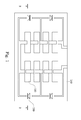
- Fig. 1 is a top view of a photovoltaic package device according to the first embodiment of the invention.
- Fig. 2 is a cross-sectional view of the photovoltaic package along the section line 2-2 of Fig. 1 .
- a photovoltaic package device includes a substrate 110, a plurality of photovoltaic cells 120, a plurality of electric devices 130, a cover 140 and an encapsulating material 150.
- the photovoltaic cells 120 are disposed on the substrate 110.
- the electric devices 130 are disposed on the substrate 110 and are electrically connected to the photovoltaic cells 120.
- the cover 140 covers the substrate 110, the photovoltaic cells 120, and the electric devices 130.
- the cover 140 includes a first depression 149 in which is received at least a portion of the electric devices 130.
- the electric devices 130 are disposed on the substrate 110 and around the photovoltaic cells 120 or at two opposite sides of the photovoltaic cells 120. Consequently, the first depression 149 corresponding to the electric devices 130 can be disposed around or at two opposite sides of the cover 140.
- the encapsulating material 150 is located between the substrate 110 and the cover 140 and at least partially encapsulates the photovoltaic cells 120 and the electric devices 130.
- the term "on” herein represents “on or above”. For example, if the photovoltaic cells 120 are described as being disposed on the substrate 110, this indicates that the photovoltaic cells 120 are disposed on or above the substrate 110. That is, the photovoltaic cells 120 can contact the substrate 110 or can be spaced apart from the substrate 110.
- the first depression 149 can receive at least a portion of the electrical devices 130, the height difference between such a portion of the electrical devices 130 and the photovoltaic cells 120 can be compensated for.
- This design can make an encapsulating process easier and also reduces the chance of breakage during manufacture.
- the first depression 149 can receive at least a portion of the electrical devices 130, the total thickness of the photovoltaic package will not increase even though the electrical devices 130 have a greater height than the photovoltaic cells 120.
- the material of the above substrate 110 can be glass, plastic or any combination thereof.
- tempered glass polyvinyl fluoride(PVF, e.g. tedlar® produced by Dupont), polyethylene terephthalate(PET), polyethylene naphthalate(PEN), or any combination thereof can be used for the material of the substrate 110.
- PVF polyvinyl fluoride
- PET polyethylene terephthalate
- PEN polyethylene naphthalate
- each of the photovoltaic cells 120 can be a monocrystalline silicon photovoltaic cell, a polycrystalline silicon photovoltaic cell, an amorphous silicon photovoltaic cell, a cadmium telluride photovoltaic cell, a copper Indium selenide photovoltaic cell, a gallium arsenide photovoltaic cell, a photochemical cell, a die-sensitized photovoltaic cell, a polymer photovoltaic cell, a nanocrystalline photovoltaic cell, or any combination thereof.
- the different types of photovoltaic cells that can be used for the photovoltaic cells 120 are mentioned by way of example, and do not limit the invention. Persons skilled in the art may select such aspects of the photovoltaic cells 120 in a flexible manner and depending on actual requirements.
- each of the electrical devices 130 can be a control circuit unit, a bypass circuit unit, a diode, a maximum power point tracking charge controller or any combination thereof.
- the electric devices 130 have a greater height than the photovoltaic cells 120.
- the height of the electric device 130 can be approximately 0.7 mm, while the height of each of the photovoltaic cells 120 can be approximately 0.2 mm.
- the material of the cover 140 can be glass, plastic or any combination thereof.
- tempered glass polyvinyl fluoride(PVF, e.g. tedlar® produced by Dupont), polyethylene terephthalate(PET), polyethylene naphthalate(PEN), or any combination thereof can be used for the material of the cover 140.
- PVF polyvinyl fluoride
- PET polyethylene terephthalate
- PEN polyethylene naphthalate
- the cover 140 can be a unibody glass or plastic. During manufacture, manufactures can choose to form the cover 140 and the first depression 149 together in a molding process or to manufacture the cover 140 in a molding process first and then the first depression 149 using a cutting process.
- the encapsulating material 150 can be any water-resistant material that is able to prevent oxygen penetration, and that also prevents breakage of the photovoltaic cells 120 and combines the cover 140 and the substrate 110.
- ethylene vinyl acetate(EVA), epoxy or any combination thereof may be used as the material for the encapsulating material 150.
- EVA ethylene vinyl acetate
- the materials used for the encapsulating material 150 are mentioned by way of example, and do not limit the invention. Persons skilled in the art may select such aspects of the encapsulating material 150 in a flexible manner and depending on actual requirements.
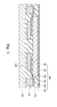
- Fig. 3 is a cross-sectional view of the photovoltaic package device according to the second embodiment of the invention. The location where the cross section is taken is the same as Fig. 2 .
- a cover 160 of this embodiment includes a photovoltaic cell cover 162 and an electric device cover 164.
- the photovoltaic cell cover 162 covers the photovoltaic cells 120.
- the electric device cover 164 extends from the side edge of the photovoltaic cell cover 162 and covers the electric devices 130.
- the electric device cover 164 is disposed around or at two opposite sides of the photovoltaic cell cover 162.
- the photovoltaic cell cover 162 is thicker than the electric device cover 164, and as a result, the edge of the photovoltaic cell cover 162 and the electric device cover 164 are on different levels (i.e., they have different heights).
- a side surface 163 of the photovoltaic cell cover 162 next to the electric device cover 164 and an inner surface 165 of the electric device cover 164 facing the electric device 130 form a first depression 169.
- the material of the photovoltaic cell cover 162 and the electric device cover 164 can be glass, plastic or any combination thereof.
- tempered glass, polyvinyl fluoride(PVF, e.g. tedlar® produced by Dupont), polyethylene terephthalate(PET), polyethylene naphthalate(PEN), or any combination thereof can be used for the material of the photovoltaic cell cover 162 and the electric device cover.
- PVF polyvinyl fluoride
- PET polyethylene terephthalate
- PEN polyethylene naphthalate
- the material of the photovoltaic cell cover 162 and that for the electric device cover 164 can be the same or different.
- the material of the photovoltaic cell cover 162 can be tempered glass and the material of the electric device cover 164 can be polyethylene terephthalate(PET).
- the cover 160 considering that manufacturing the cover 160 as a unibody is difficult, manufacturers can produce the photovoltaic cell cover 162 and the electric device cover 164 separately, then utilize an adhesive 166 to bond the photovoltaic cell cover 162 and the electric device cover 164.
- the particular type of the adhesive 166 used depends on the material of the photovoltaic cell cover 162 and that of the electric device cover 164, and it is necessary only that the adhesive 166 is able to bond the photovoltaic cell cover 162 and the electric device cover 164.
- the adhesive 166 can be, but is not limited to being, a double-sided tape, a tape (having an adhesive property on only one side thereof), a paper tape, silicone, epoxy resin, polyurethane adhesive, a polymethyl methacrylate (PMMA) adhesive, an encapsulating adhesive, a hot-melt adhesive, a UV adhesive, or any combination thereof.
- a double-sided tape a tape (having an adhesive property on only one side thereof)
- a paper tape silicone, epoxy resin, polyurethane adhesive, a polymethyl methacrylate (PMMA) adhesive, an encapsulating adhesive, a hot-melt adhesive, a UV adhesive, or any combination thereof.
- PMMA polymethyl methacrylate
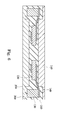
- Fig. 4 is a cross-sectional view of the photovoltaic package device according to the third embodiment of the invention. The location where the cross section is taken is the same as Fig. 2 .
- the photovoltaic package of this embodiment further includes a frame 170 an assembly of the substrate 110, the photovoltaic cells 120, the electric devices 130, the cover 160, and the encapsulating material 150 is disposed in the frame 170. Edges of the frame 170 cover the border between the photovoltaic cell cover 162 and the electric device cover 164.
- the frame 170 can be a part of the housing of the electric device.
- the material of the frame 17 can be, but is not limited to being, plastic, metal, wood, carbon fiber, leather, or any combination thereof.
- Fig. 5 is a cross-sectional view of the photovoltaic package device according to the fourth embodiment of the invention.
- the location where the cross section is taken is the same as Fig. 2 .
- the difference between this embodiment and the first embodiment in Fig. 1 and Fig. 2 is that a cover 180 of this embodiment includes an outer cover 182 and an inner cover 184.
- the outer cover 182 covers the substrate 110, the photovoltaic cells 120, and the electrical devices 130.
- the inner cover 184 is disposed between the outer cover 182 and the photovoltaic cells 120.
- a surface 183 area of the outer cover 182 is larger than a surface area 185 of the inner cover 184, and as a result, a bottom surface of the inner cover 184 and a bottom surface of the outer cover 182 are on different levels (i.e., they have different heights).
- a first depression 189 to receive a portion of the electrical devices 130 is formed by the outer and inner covers 182, 184.
- the material of the outer cover 182 and the inner cover 184 can be glass, plastic or any combination thereof.
- tempered glass, polyvinyl fluoride(PVF, e.g. tedlar® produced by Dupont), polyethylene terephthalate(PET), polyethylene naphthalate(PEN), or any combination thereof can be used for the material of the outer and inner covers 182, 184.
- PVF polyvinyl fluoride
- PET polyethylene terephthalate
- PEN polyethylene naphthalate
- Persons skilled in the art may select such aspects of the outer cover 182 and the inner cover 184 in a flexible manner and depending on actual requirements.
- the material of the outer cover 182 and that for the inner cover 184 can be the same or different.
- the material for each of the outer cover 182 and the inner cover 184 can be tempered glass.
- the inner cover 184 can be tempered glass, while the outer cover 182 can be polyethylene terephthalate(PET).
- the cover 180 considering that manufacturing the cover 180 as a unibody is difficult, manufacturers can produce the outer cover 182 and the inner cover 184 separately, then use an adhesive 186 to bond the outer cover 182 and the inner cover 184.
- the particular type of the adhesive 186 used depends on the material of the outer cover 182 and that of the inner cover 184, and it is necessary only that the adhesive 186 is able to bond the outer cover 182 and the inner cover 184.
- the adhesive 186 can be, but is not limited to being, a double-sided tape, a tape (having an adhesive property on only one side thereof), a paper tape, silicone, epoxy resin, polyurethane adhesive, a polymethyl methacrylate (PMMA) adhesive, an encapsulating adhesive, a hot-melt adhesive, a UV adhesive, or any combination thereof.
- a double-sided tape a tape (having an adhesive property on only one side thereof)
- a paper tape silicone, epoxy resin, polyurethane adhesive, a polymethyl methacrylate (PMMA) adhesive, an encapsulating adhesive, a hot-melt adhesive, a UV adhesive, or any combination thereof.
- PMMA polymethyl methacrylate
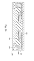
- Fig. 6 is a cross-sectional view of the photovoltaic package device according to the fifth embodiment of the invention.
- the location where the cross section is taken is the same as Fig. 2 .
- the difference between this embodiment and the first embodiment in Fig. 1 and Fig. 2 is that a substrate 200 of this embodiment includes a second depression 209.
- the electrical devices 130 are at least partially disposed in the second depression 209.
- the electric devices 130 are disposed around or at two opposite sides of a plurality of the photovoltaic cells 120 on the substrate 110. Therefore, the second depression 209, which corresponds to the electric devices 130, can be disposed around or at two opposite sides of the substrate 110.
- the first depression 149 may not be able to compensate for the height difference between the electric devices 130 and the photovoltaic cells 120.
- manufacturers can choose to further form the second depression 209 on the substrate 200 and therefore make for the inability of the first depression 149 to fully compensate for this height differential between the electric devices 130 and the photovoltaic cells 120.
- the substrate 200 can be a unibody made of glass or plastic. During manufacture, manufactures can choose to form the substrate 200 and the second depression 209 together in a molding process or manufacture the substrate 200 in a molding process first and then the second depression 209 using a cutting process.
- Fig. 7 is a cross-sectional view of the photovoltaic package device according to the sixth embodiment of the invention.
- the location where the cross section is taken is the same as Fig. 2 .
- the difference between this embodiment and the second embodiment is that a substrate 210 of this embodiment includes a photovoltaic cell base 212 and an electric device base 214.
- the photovoltaic cells 120 are disposed on and above the photovoltaic cell base 212.
- the electric device base 214 extends from the side edge of the photovoltaic cell base 212.
- the electric device base 214 can be disposed around or at opposite sides of the photovoltaic cell base 212.
- the photovoltaic cell base 212 is thicker than the electric device base 214, and as a result, the photovoltaic cell base 212 and the electric device base 214 are on different levels (i.e., they have different heights) and form a second depression 219.
- a side surface 213 of the photovoltaic cell base 212 next to the electric device base 214 and an inner surface 215 of the electric device base 214 facing the electric devices 130 form a second depression 219.
- the material of the photovoltaic cell base 212 and the electric device base 214 can be glass, plastic or any combination thereof.
- tempered glass, polyvinyl fluoride(PVF, e.g. tedlar® produced by Dupont), polyethylene terephthalate(PET), polyethylene naphthalate(PEN), or any combination thereof can be used for the material of the photovoltaic cell base 212 and the electric device base 214.
- PVF polyvinyl fluoride
- PET polyethylene terephthalate
- PEN polyethylene naphthalate
- Persons skilled in the art may select such aspects of the photovoltaic cell base 212 and the electric device base 214 in a flexible manner and depending on actual requirements.
- the material of the photovoltaic cell base 212 and the electric device base 214 can be the same or different.
- the material of the photovoltaic cell base 212 and the electric device base 214 can be tempered glass.
- the photovoltaic cell base 212 can be tempered glass, while the electric device base 214 can be polyethylene terephthalate(PET).
- the cover 180 considering that manufacturing the cover 180 as a unibody is difficult, manufacturers can produce the photovoltaic cell base 212 and the electric device base 214 separately, then use an adhesive 216 to bond the photovoltaic cell base 212 and the electric device base 214.
- the particular type of the adhesive 216 used depends on the material of the photovoltaic cell base 212 and that of the electric device base 214, and it is necessary only that the adhesive 216 is able to bond the photovoltaic cell base 212 and the electric device base 214.
- the adhesive 216 can be, but is not limited to being, a doubled-side tape, a tape (having an adhesive property on only one side thereof), a paper tape, silicone, epoxy resin, polyurethane adhesive, a polymethyl methacrylate (PMMA) adhesive, a encapsulating adhesive, a hot-melt adhesive, a UV adhesive, or any combination thereof.
- a doubled-side tape a tape (having an adhesive property on only one side thereof)
- a paper tape silicone, epoxy resin, polyurethane adhesive, a polymethyl methacrylate (PMMA) adhesive, a encapsulating adhesive, a hot-melt adhesive, a UV adhesive, or any combination thereof.
- PMMA polymethyl methacrylate
- Fig. 8 is a cross-sectional view of the photovoltaic package device according to the seventh embodiment of the invention.
- the location where the cross section is taken is the same as Fig. 2 .
- the photovoltaic package of the embodiment further includes the frame 170, and the assembly of the substrate 210, the photovoltaic cells 120, the electric devices 130, the cover 160, and the encapsulating material 150 is disposed in the frame 170.
- the edge of the frame 170 covers not only the border between the photovoltaic cell cover 162 and the electric device cover 164 but also the border between the photovoltaic cell base 212 and the electric device base 214.
- the frame 170 can be a part of the housing of the electric device.
- the material of the frame 170 can be, but is not limited to being, plastic, metal, wood, carbon fiber, leather, or any combination thereof.
- Fig. 9 is a cross-sectional view of the photovoltaic package device according to the eighth embodiment of the invention.
- the location where the cross section is taken is the same as Fig. 2 .
- the difference between this embodiment and the fourth embodiment is that a substrate 220 of this embodiment includes an inner plate 224 and an outer plate 222.
- the photovoltaic cells 120 are disposed on the inner plate 224.
- the outer plate 222 is disposed on an outer surface 225 of the inner plate 224 with a (rear) surface 223 of the outer plate 222 facing the photovoltaic cells 120.
- the area of the surface 223 of the outer plate 222 is larger than the area of an outer surface 225 of the inner plate 224, such that the edge of the inner plate 224 and the edge of the outer plate 222 are on different levels (i.e., they have different heights) and form a second depression 229.
- the material of the inner plate 224 and the outer plate 222 can be glass, plastic or any combination thereof.
- tempered glass, polyvinyl fluoride(PVF, e.g. tedlar® produced by Dupont), polyethylene terephthalate(PET), polyethylene naphthalate(PEN), or any combination thereof can be used for the material of the inner plate 224 and the outer plate 222.
- PVF polyvinyl fluoride
- PET polyethylene terephthalate
- PEN polyethylene naphthalate
- Persons skilled in the art may select such aspects of the inner plate 224 and the outer plate 222 in a flexible manner and depending on actual requirements.
- the material of the inner plate 224 and that for the outer plate 222 can be the same or different.
- the material of the inner plate 224 and the outer plate 222 can be tempered glass.
- the inner plate 224 and the outer plate 222 can be polyethylene terephthalate(PET).
- manufacturers can produce the inner plate 224 and the outer plate 222 separately, then use an adhesive 226 to bond the inner plate 224 and the outer plate 222.
- the particular type of the adhesive 226 used depends on the material of the inner plate 224 and that of the outer plate 222, and it is necessary only that the adhesive 226 is able to bond the inner plate 224 and the outer plate 222.
- the adhesive 226 can be, but is not limited to being, a double-sided tape, a tape (having an adhesive property on only one side thereof), a paper tape, silicone, epoxy resin, polyurethane adhesive, a polymethyl methacrylate (PMMA) adhesive, an encapsulating adhesive, a hot-melt adhesive, a UV adhesive, or any combination thereof.
- a double-sided tape a tape (having an adhesive property on only one side thereof)
- a paper tape silicone, epoxy resin, polyurethane adhesive, a polymethyl methacrylate (PMMA) adhesive, an encapsulating adhesive, a hot-melt adhesive, a UV adhesive, or any combination thereof.
- PMMA polymethyl methacrylate
- Fig. 10 is a cross-sectional view of the photovoltaic package device according to the ninth embodiment of the invention.
- the location where the cross section is taken is the same as Fig. 2 .
- the difference between this embodiment and the fifth embodiment is that the second depression 209 is disposed only on the substrate 200, and the cover 190 is not formed with any depression.
- a configuration can be used in which the substrate 200 in Fig. 6 and Fig. 10 is combined with the cover 140 in Fig. 6 or the cover 190 designed without a depression in Fig. 10 .
- a configuration can be used in which the substrate 200 in Fig. 6 and Fig. 10 is combined with the cover 160 in Fig. 7 or the cover 180 in Fig. 9 .
- Persons skilled in the art may select such aspects of the substrate and the cover in a flexible manner and depending on actual requirements.
- Fig. 11 is a cross-sectional view of the photovoltaic package device according to the tenth embodiment of the invention.
- the location where the cross section is taken is the same as Fig. 2 .
- the difference between this embodiment and the fifth embodiment is that the second depression 219 is disposed only on the substrate 210, and the cover 190 is not formed with any depression.
- a configuration can be used in which the substrate 210 in Fig. 7 and Fig. 11 is combined with the cover 160 in Fig. 7 or the cover 190 designed without a depression in Fig. 11 .
- a configuration can be used in which the substrate 210 in Fig. 7 and Fig. 11 is combined with the cover 140 in Fig. 6 or the cover 180 in Fig. 9 .
- Persons skilled in the art may select such aspects of the substrate and the cover in a flexible manner and depending on actual requirements.
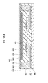
- Fig. 12 is a cross-sectional view of the photovoltaic package device according to the eleventh embodiment of the invention. The location where the cross section is taken is the same as Fig. 2 .
- the difference between this embodiment and the seventh embodiment is that the second depression 219 is disposed only on the substrate 210, and the cover 190 is not formed with a depression.
- Fig. 13 is a cross-sectional view of the photovoltaic package device according to the twelfth embodiment of the invention.
- the location where the cross section is taken is the same as Fig. 2 .
- the difference between this embodiment and the eighth embodiment is that the second depression 229 is disposed only on the substrate 220, and the cover 190 is not formed with a first depression.
- a configuration can be used in which the substrate 220 in Fig. 9 and Fig. 13 is combined with the cover 180 in Fig. 9 or the cover 190 designed without a depression in Fig. 13 .
- a configuration can be used in which the substrate 220 in Fig. 9 and Fig. 13 is combined with the cover 140 in Fig. 6 or the cover 160 in Fig. 7 .
- Persons skilled in the art may select such aspects of the substrate and the cover in a flexible manner and depending on actual requirements.
Landscapes
- Photovoltaic Devices (AREA)
Applications Claiming Priority (1)
| Application Number | Priority Date | Filing Date | Title |
|---|---|---|---|
| TW100137399A TWI563673B (en) | 2011-10-14 | 2011-10-14 | Photovoltaic package |
Publications (2)
| Publication Number | Publication Date |
|---|---|
| EP2581945A2 true EP2581945A2 (de) | 2013-04-17 |
| EP2581945A3 EP2581945A3 (de) | 2015-02-11 |
Family
ID=45985192
Family Applications (1)
| Application Number | Title | Priority Date | Filing Date |
|---|---|---|---|
| EP12174855.2A Withdrawn EP2581945A3 (de) | 2011-10-14 | 2012-07-03 | Photovoltaikpackung |
Country Status (4)
| Country | Link |
|---|---|
| US (1) | US20130092231A1 (de) |
| EP (1) | EP2581945A3 (de) |
| CN (1) | CN102437217A (de) |
| TW (1) | TWI563673B (de) |
Cited By (1)
| Publication number | Priority date | Publication date | Assignee | Title |
|---|---|---|---|---|
| CN109921096A (zh) * | 2019-03-07 | 2019-06-21 | 广东鸿宝科技有限公司 | 一种带保液量闭环控制的电池封口机及其控制方法 |
Families Citing this family (8)
| Publication number | Priority date | Publication date | Assignee | Title |
|---|---|---|---|---|
| DE102012224432A1 (de) * | 2012-12-27 | 2014-04-10 | Robert Bosch Gmbh | Elektrische Schaltung und Verfahren zum Herstellen einer elektrischen Schaltung |
| KR101534971B1 (ko) * | 2013-12-19 | 2015-07-07 | 현대자동차주식회사 | 자동차용 염료감응 태양전지의 곡면화 방법 |
| CN105811589A (zh) * | 2014-12-31 | 2016-07-27 | tealstone责任有限公司 | 一种可再生能源模块及其制备方法 |
| CN105846482A (zh) * | 2015-01-13 | 2016-08-10 | tealstone责任有限公司 | 一种基于可再生能源模块的充电装置 |
| WO2017210570A1 (en) * | 2016-06-03 | 2017-12-07 | Suncore Photovoltaics, Inc. | Solar receiver with cover glass |
| WO2020033371A1 (en) * | 2018-08-06 | 2020-02-13 | Solar Hardscapes Llc | Landscape pavers for ground installation of photovoltaic panels, landscape paver installations, and installation methods |
| CN111354813B (zh) * | 2020-04-20 | 2026-01-27 | 珠海格力电器股份有限公司 | 光伏组件及其制造方法 |
| EP4216285A4 (de) * | 2020-09-15 | 2024-07-03 | Kabushiki Kaisha Toshiba | Solarzelle |
Family Cites Families (7)
| Publication number | Priority date | Publication date | Assignee | Title |
|---|---|---|---|---|
| GB2247564B (en) * | 1990-08-16 | 1995-01-04 | Eev Ltd | A solar cell arrangement |
| JP3979829B2 (ja) * | 2001-11-28 | 2007-09-19 | 旭化成建材株式会社 | 瓦一体型太陽電池モジュール |
| JP5404987B2 (ja) * | 2005-09-13 | 2014-02-05 | 三洋電機株式会社 | 太陽電池モジュール |
| KR100680654B1 (ko) * | 2006-08-07 | 2007-02-08 | 해성쏠라(주) | 발광소자가 일체형으로 구비된 태양전지모듈 |
| WO2008154524A2 (en) * | 2007-06-08 | 2008-12-18 | Robert Stancel | Edge mountable electrical connection assembly |
| JP2009088406A (ja) * | 2007-10-02 | 2009-04-23 | Sanyo Electric Co Ltd | 太陽電池及びその製造方法 |
| EP2320471A4 (de) * | 2008-08-08 | 2015-11-04 | Sphelar Power Corp | Tageslicht-solarbatteriemodul |
-
2011
- 2011-10-14 TW TW100137399A patent/TWI563673B/zh not_active IP Right Cessation
- 2011-11-17 CN CN2011103749013A patent/CN102437217A/zh active Pending
-
2012
- 2012-06-14 US US13/523,078 patent/US20130092231A1/en not_active Abandoned
- 2012-07-03 EP EP12174855.2A patent/EP2581945A3/de not_active Withdrawn
Non-Patent Citations (1)
| Title |
|---|
| None |
Cited By (2)
| Publication number | Priority date | Publication date | Assignee | Title |
|---|---|---|---|---|
| CN109921096A (zh) * | 2019-03-07 | 2019-06-21 | 广东鸿宝科技有限公司 | 一种带保液量闭环控制的电池封口机及其控制方法 |
| CN109921096B (zh) * | 2019-03-07 | 2024-02-23 | 广东鸿宝科技有限公司 | 一种电池封口机的电解液保液量闭环控制方法 |
Also Published As
| Publication number | Publication date |
|---|---|
| EP2581945A3 (de) | 2015-02-11 |
| CN102437217A (zh) | 2012-05-02 |
| TW201316533A (zh) | 2013-04-16 |
| TWI563673B (en) | 2016-12-21 |
| US20130092231A1 (en) | 2013-04-18 |
Similar Documents
| Publication | Publication Date | Title |
|---|---|---|
| EP2581945A2 (de) | Photovoltaikpackung | |
| US9948232B2 (en) | Method for fabricating flexible solar panel module | |
| US20120152327A1 (en) | Method of manufacturing solar modules | |
| ZA200607745B (en) | Electric energy generating modules with a two-dimensional profile and method of fabricating the same | |
| CN110959198A (zh) | 稳定的叠瓦状太阳能电池串及其生产方法 | |
| JP6038883B2 (ja) | 分極を防止するための太陽電池モジュール構造及び製造方法 | |
| JP2007123725A (ja) | Cis系薄膜太陽電池モジュール及びその製造方法 | |
| US11424714B2 (en) | Angled polymer solar modules | |
| EP2360741A2 (de) | Photovoltaikmodul und Verfahren zu dessen Herstellung | |
| US20170117428A1 (en) | Flexible Solar Panel Module | |
| US20150288323A1 (en) | Flexible building-integrated photovoltaic structure | |
| KR101594841B1 (ko) | 태양전지 모듈 및 이의 제조방법 | |
| US20130298969A1 (en) | Solar module | |
| US20110155245A1 (en) | Solar module having a side insulating member | |
| CN204760395U (zh) | 可挠式太阳能板模块及其固定结构 | |
| US20160043249A1 (en) | Solar cell module and method of fabricating the same | |
| US20140318603A1 (en) | All Plastic Solar Panel | |
| US20140158200A1 (en) | Solar module | |
| CN105556683B (zh) | 太阳能电池模块 | |
| US20120024339A1 (en) | Photovoltaic Module Including Transparent Sheet With Channel | |
| KR20140121920A (ko) | 태양전지 모듈 및 그 제조방법 | |
| CN105849474A (zh) | 太阳能电池组件 | |
| KR20150049259A (ko) | 정션 박스 및 이를 구비한 태양광 모듈 | |
| US9685574B2 (en) | Solar cell module | |
| JP6156718B2 (ja) | 太陽電池パネル |
Legal Events
| Date | Code | Title | Description |
|---|---|---|---|
| PUAI | Public reference made under article 153(3) epc to a published international application that has entered the european phase |
Free format text: ORIGINAL CODE: 0009012 |
|
| 17P | Request for examination filed |
Effective date: 20120703 |
|
| AK | Designated contracting states |
Kind code of ref document: A2 Designated state(s): AL AT BE BG CH CY CZ DE DK EE ES FI FR GB GR HR HU IE IS IT LI LT LU LV MC MK MT NL NO PL PT RO RS SE SI SK SM TR |
|
| AX | Request for extension of the european patent |
Extension state: BA ME |
|
| PUAL | Search report despatched |
Free format text: ORIGINAL CODE: 0009013 |
|
| AK | Designated contracting states |
Kind code of ref document: A3 Designated state(s): AL AT BE BG CH CY CZ DE DK EE ES FI FR GB GR HR HU IE IS IT LI LT LU LV MC MK MT NL NO PL PT RO RS SE SI SK SM TR |
|
| AX | Request for extension of the european patent |
Extension state: BA ME |
|
| RIC1 | Information provided on ipc code assigned before grant |
Ipc: H01L 31/042 20140101AFI20150107BHEP |
|
| 17Q | First examination report despatched |
Effective date: 20160421 |
|
| STAA | Information on the status of an ep patent application or granted ep patent |
Free format text: STATUS: THE APPLICATION IS DEEMED TO BE WITHDRAWN |
|
| 18D | Application deemed to be withdrawn |
Effective date: 20160902 |