EP2582029A2 - Schaltender Umrichter mit Längsreglerschutz für Transienten - Google Patents
Schaltender Umrichter mit Längsreglerschutz für Transienten Download PDFInfo
- Publication number
- EP2582029A2 EP2582029A2 EP12188531.3A EP12188531A EP2582029A2 EP 2582029 A2 EP2582029 A2 EP 2582029A2 EP 12188531 A EP12188531 A EP 12188531A EP 2582029 A2 EP2582029 A2 EP 2582029A2
- Authority
- EP
- European Patent Office
- Prior art keywords
- current
- voltage
- over
- power
- supply modulator
- Prior art date
- Legal status (The legal status is an assumption and is not a legal conclusion. Google has not performed a legal analysis and makes no representation as to the accuracy of the status listed.)
- Granted
Links
Images






Classifications
-
- H—ELECTRICITY
- H02—GENERATION; CONVERSION OR DISTRIBUTION OF ELECTRIC POWER
- H02H—EMERGENCY PROTECTIVE CIRCUIT ARRANGEMENTS
- H02H7/00—Emergency protective circuit arrangements specially adapted for specific types of electric machines or apparatus or for sectionalised protection of cable or line systems, and effecting automatic switching in the event of an undesired change from normal working conditions
- H02H7/10—Emergency protective circuit arrangements specially adapted for specific types of electric machines or apparatus or for sectionalised protection of cable or line systems, and effecting automatic switching in the event of an undesired change from normal working conditions for converters; for rectifiers
- H02H7/12—Emergency protective circuit arrangements specially adapted for specific types of electric machines or apparatus or for sectionalised protection of cable or line systems, and effecting automatic switching in the event of an undesired change from normal working conditions for converters; for rectifiers for static converters or rectifiers
- H02H7/122—Emergency protective circuit arrangements specially adapted for specific types of electric machines or apparatus or for sectionalised protection of cable or line systems, and effecting automatic switching in the event of an undesired change from normal working conditions for converters; for rectifiers for static converters or rectifiers for inverters, i.e. DC/AC converters
-
- H—ELECTRICITY
- H02—GENERATION; CONVERSION OR DISTRIBUTION OF ELECTRIC POWER
- H02M—APPARATUS FOR CONVERSION BETWEEN AC AND AC, BETWEEN AC AND DC, OR BETWEEN DC AND DC, AND FOR USE WITH MAINS OR SIMILAR POWER SUPPLY SYSTEMS; CONVERSION OF DC OR AC INPUT POWER INTO SURGE OUTPUT POWER; CONTROL OR REGULATION THEREOF
- H02M3/00—Conversion of DC power input into DC power output
- H02M3/02—Conversion of DC power input into DC power output without intermediate conversion into AC
- H02M3/04—Conversion of DC power input into DC power output without intermediate conversion into AC by static converters
- H02M3/10—Conversion of DC power input into DC power output without intermediate conversion into AC by static converters using discharge tubes with control electrode or semiconductor devices with control electrode
- H02M3/145—Conversion of DC power input into DC power output without intermediate conversion into AC by static converters using discharge tubes with control electrode or semiconductor devices with control electrode using devices of a triode or transistor type requiring continuous application of a control signal
- H02M3/155—Conversion of DC power input into DC power output without intermediate conversion into AC by static converters using discharge tubes with control electrode or semiconductor devices with control electrode using devices of a triode or transistor type requiring continuous application of a control signal using semiconductor devices only
- H02M3/156—Conversion of DC power input into DC power output without intermediate conversion into AC by static converters using discharge tubes with control electrode or semiconductor devices with control electrode using devices of a triode or transistor type requiring continuous application of a control signal using semiconductor devices only with automatic control of output voltage or current, e.g. switching regulators
- H02M3/158—Conversion of DC power input into DC power output without intermediate conversion into AC by static converters using discharge tubes with control electrode or semiconductor devices with control electrode using devices of a triode or transistor type requiring continuous application of a control signal using semiconductor devices only with automatic control of output voltage or current, e.g. switching regulators including plural semiconductor devices as final control devices for a single load
-
- H—ELECTRICITY
- H02—GENERATION; CONVERSION OR DISTRIBUTION OF ELECTRIC POWER
- H02M—APPARATUS FOR CONVERSION BETWEEN AC AND AC, BETWEEN AC AND DC, OR BETWEEN DC AND DC, AND FOR USE WITH MAINS OR SIMILAR POWER SUPPLY SYSTEMS; CONVERSION OF DC OR AC INPUT POWER INTO SURGE OUTPUT POWER; CONTROL OR REGULATION THEREOF
- H02M1/00—Details of apparatus for conversion
- H02M1/32—Means for protecting converters other than automatic disconnection
-
- H—ELECTRICITY
- H02—GENERATION; CONVERSION OR DISTRIBUTION OF ELECTRIC POWER
- H02M—APPARATUS FOR CONVERSION BETWEEN AC AND AC, BETWEEN AC AND DC, OR BETWEEN DC AND DC, AND FOR USE WITH MAINS OR SIMILAR POWER SUPPLY SYSTEMS; CONVERSION OF DC OR AC INPUT POWER INTO SURGE OUTPUT POWER; CONTROL OR REGULATION THEREOF
- H02M1/00—Details of apparatus for conversion
- H02M1/0045—Converters combining the concepts of switch-mode regulation and linear regulation, e.g. linear pre-regulator to switching converter, linear and switching converter in parallel, same converter or same transistor operating either in linear or switching mode
-
- H—ELECTRICITY
- H02—GENERATION; CONVERSION OR DISTRIBUTION OF ELECTRIC POWER
- H02M—APPARATUS FOR CONVERSION BETWEEN AC AND AC, BETWEEN AC AND DC, OR BETWEEN DC AND DC, AND FOR USE WITH MAINS OR SIMILAR POWER SUPPLY SYSTEMS; CONVERSION OF DC OR AC INPUT POWER INTO SURGE OUTPUT POWER; CONTROL OR REGULATION THEREOF
- H02M3/00—Conversion of DC power input into DC power output
- H02M3/02—Conversion of DC power input into DC power output without intermediate conversion into AC
- H02M3/04—Conversion of DC power input into DC power output without intermediate conversion into AC by static converters
- H02M3/10—Conversion of DC power input into DC power output without intermediate conversion into AC by static converters using discharge tubes with control electrode or semiconductor devices with control electrode
- H02M3/145—Conversion of DC power input into DC power output without intermediate conversion into AC by static converters using discharge tubes with control electrode or semiconductor devices with control electrode using devices of a triode or transistor type requiring continuous application of a control signal
- H02M3/155—Conversion of DC power input into DC power output without intermediate conversion into AC by static converters using discharge tubes with control electrode or semiconductor devices with control electrode using devices of a triode or transistor type requiring continuous application of a control signal using semiconductor devices only
- H02M3/156—Conversion of DC power input into DC power output without intermediate conversion into AC by static converters using discharge tubes with control electrode or semiconductor devices with control electrode using devices of a triode or transistor type requiring continuous application of a control signal using semiconductor devices only with automatic control of output voltage or current, e.g. switching regulators
- H02M3/1566—Conversion of DC power input into DC power output without intermediate conversion into AC by static converters using discharge tubes with control electrode or semiconductor devices with control electrode using devices of a triode or transistor type requiring continuous application of a control signal using semiconductor devices only with automatic control of output voltage or current, e.g. switching regulators with means for compensating against rapid load changes, e.g. with auxiliary current source, with dual mode control or with inductance variation
Definitions
- the present invention relates to a supply modulator.
- a supply modulator is a device for modulating Direct Current (DC) power to supply Alternating Current (AC) power that changes in accordance with an input signal to a load.
- the supply modulator is primarily utilized in a mobile communication terminal for converting an input baseband signal to an output Radio Frequency (RF) signal at high efficiency using limited battery power.
- RF Radio Frequency
- PAPR Peak to Average Power Ratio
- a supply modulator that independently applies a linear regulator or a Switching Mode Power Supplier (SMPS) technology primarily utilized as a DC-DC converter in a power Integrated Circuit (IC) field has been realized.
- SMPS Switching Mode Power Supplier
- IC power Integrated Circuit
- an aspect of the present invention is to provide an apparatus and a method for recognizing an electric over-stress situation of a supply modulator.
- Another aspect of the present invention is to provide an apparatus and a method for protecting a network of a supply modulator.
- Still another aspect of the present invention is to provide an apparatus and a method for recognizing an electric over-stress situation of a hybrid supply modulator.
- Yet another aspect of the present invention is to provide an apparatus and a method for protecting a network of a hybrid supply modulator.
- a further aspect of the present invention is to provide an apparatus and a method for recognizing an in-current situation due to power unbalance in a hybrid supply modulator.
- a yet further aspect of the present invention is to provide an apparatus and a method for recognizing an over-current situation due to a load short in a hybrid supply modulator.
- a still further aspect of the present invention is to provide an apparatus and a method for recognizing an over-current situation due to a load open in a hybrid supply modulator.
- Still yet another aspect of the present invention is to provide an apparatus and a method for recognizing an over-voltage situation of an output in a hybrid supply modulator.
- a hybrid supply modulator apparatus including a Switching Mode Power Supplier (SMPS) for generating a current of a modulated power signal and a linear regulator for generating a sourcing current for supplementing a shortage amount of a current generated by the SMPS and generating a sinking current for removing an excessive amount of the current is provided.
- SMPS Switching Mode Power Supplier
- the apparatus includes at least one sensing unit for sensing at least one of a current and a voltage at one or more points defined in advance within a supply modulator network, and at least one actuator unit for performing a protection action corresponding to at least one electric over-stress situation represented by the sensing result
- the SMPS includes a driver for controlling at least one switch device depending on an input signal, at least one switch device for controlling an amount of a current under control of the driver, and a filter for filtering a signal passing through the switch device
- the linear regulator includes a first transistor for generating the sourcing current, a second transistor for generating the sinking current, and an amplifier for controlling an amount of a current generated by the first transistor and the second transistor.
- a method for operating a hybrid supply modulator including a SMPS for generating a current of a modulated power signal and a linear regulator for generating a sourcing current for supplementing a shortage amount of a current generated by the SMPS and generating a sinking current for removing an excessive amount of the current is provided.
- the method includes sensing at least one of a current and a voltage at one or more points defined in advance within a supply modulator circuit, and performing a protection action corresponding to at least one electric over-stress situation represented by the sensing result, wherein the SMPS includes a driver for controlling at least one switch device depending on an input signal, at least one switch device for controlling an amount of a current under control of the driver, and a filter for filtering a signal passing through the switch device, and wherein the linear regulator includes a first transistor for generating the sourcing current, a second transistor for generating the sinking current, and an amplifier for controlling an amount of a current generated by the first transistor and the second transistor.
- FIG. 1 is a block diagram illustrating a hybrid supply modulator according to an exemplary embodiment of the present invention
- FIG. 2 is a view illustrating an in-current generated by a hybrid supply modulator according to an exemplary embodiment of the present invention
- FIG. 3 is a graph illustrating measurement results of an in-current generated by a supply modulator according to an exemplary embodiment of the present invention
- FIG. 4 is a block diagram illustrating a supply modulator according to an exemplary embodiment of the present invention.
- FIG. 5 is a block diagram illustrating a first voltage sensor of a supply modulator according to an exemplary embodiment of the present invention
- FIG. 6 is a graph illustrating a current waveform of a supply modulator according to an exemplary embodiment of the present invention.
- FIG. 7 is a block diagram illustrating a first current sensor of a supply modulator according to an exemplary embodiment of the present invention.
- FIG. 8 is a block diagram illustrating a logic unit of a supply modulator according to an exemplary embodiment of the present invention.
- FIG. 9 is a block diagram illustrating a second current sensor and a bypass unit of a supply modulator according to an exemplary embodiment of the present invention.
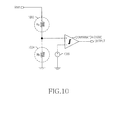
- FIG. 10 is a block diagram illustrating a second voltage sensor of a supply modulator according to an exemplary embodiment of the present invention.
- FIG. 11 is a flowchart illustrating a protection procedure from an in-current of a supply modulator according to an exemplary embodiment of the present invention
- FIG. 12 is a flowchart illustrating a protection procedure from an over-current by load short of a supply modulator according to an exemplary embodiment of the present invention
- FIG. 13 is a flowchart illustrating a protection procedure from an over-current by load open of a supply modulator according to an exemplary embodiment of the present invention
- FIG. 14 is a flowchart illustrating a protection procedure from an over-voltage output of a supply modulator according to an exemplary embodiment of the present invention
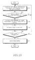
- FIG. 15 is a flowchart illustrating a protection procedure from an in-current, over-temperature, a battery low voltage/high voltage during an operation of a supply modulator according to an exemplary embodiment of the present invention.
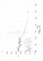
- FIG. 16 is a graph illustrating a current waveform of a hybrid supply modulator according to an exemplary embodiment of the present invention.
- the present invention relates to recognizing an electric over-stress situation of a supply modulator.
- Exemplary embodiments of the present invention relate to an apparatus and a method for recognizing an electric over-stress situation in a supply modulator and protecting a network of the supply modulator from the electric over-stress.
- Exemplary embodiments of the present invention provide a technology for recognizing an electric over-stress of a hybrid supply modulator configured by coupling of a linear regulator and a Switching Mode Power Supplier (SMPS), and protecting a circuit.
- SMPS Switching Mode Power Supplier
- FIG. 1 is a block diagram illustrating a hybrid supply modulator according to an exemplary embodiment of the present invention.
- the hybrid supply modulator includes a linear regulator core 110 and an SMPS core 120.
- Respective outputs of the linear regulator core 110 and the SMPS core 120 are coupled, so that one supply modulator output is generated.
- Information of a signal input, which is one source, is shared in various ways, so that control information may be configured to control the linear regulator core 110 and the SMPS core 120.
- the linear regulator core 110 includes an Operational Amplifier (OP AMP) 111, a first feedback network 112, a second feedback network 113, an upper pass transistor 114, and a lower pass transistor 115.
- the upper pass transistor 114 is a P-channel Metal-Oxide-Semiconductor (PMOS) transistor. A source is connected to power, a gate is connected to the OP AMP 111, and a drain is connected to an output terminal of the linear regulator core 110.
- the lower pass transistor 114 is an N-channel Metal-Oxide-Semiconductor (NMOS) transistor. A drain is connected to an output terminal of the linear regulator core 110, a gate is connected to the OP AMP 111, and a source is connected to a ground.
- NMOS N-channel Metal-Oxide-Semiconductor
- the linear regulator core 110 linearly converts an input voltage signal by regulating an output voltage of pass transistors 114 and 115 via a feedback loop configured with the feedback networks 112 and 113 depending on an input signal input to the OP AMP 111.
- the SMPS core 120 includes an upper switch transistor 121, a lower switch transistor 122, an inductor 123, a capacitor 124, a third feedback network 125, a comparator 126, and a switch driver 127.
- the upper switch transistor 121 is a PMOS transistor. A source is connected to power, a gate is connected to the switch driver 127, and a drain is connected to the inductor 123.
- the lower switch transistor 122 is an NMOS transistor. A drain is connected to the inductor 123, a gate is connected to the switch driver 127, and a source is connected to the ground.
- An output of the SMPS core 120 is scaled by the third feedback network 125, and then provided to the comparator 126.
- the comparator 126 compares an input signal with the scaled output signal.
- the switch driver 127 regulates an amount of a current supplied to a load 130 by controlling a switching frequency of the switch transistors 121 and 122 or an on-off duty ratio depending on a comparison result of the comparator 126. Specifically, when the output signal is greater than the input signal, the switch driver 127 turns off the upper switch transistor 121 and turns on the lower switch transistor 122 in order to reduce a current of the output signal.
- the switch driver 127 turns on the upper switch transistor 121 and turns off the lower switch transistor 122 in order to increase a current of the output signal. That is, the switch transistors 121 and 122 regulate a current amount of the output signal under the control of the switch driver 127.
- a Pulse Frequency Modulation (PFM) signal or a Pulse Width Modulation (PWM) signal is generated by the switch transistors 121 and 122.
- a signal supplied to the load 130 via the switch transistors 121 and 122 is filtered by a Low Pass Filter (LPF) configured with the inductor 123 and the capacitor 124 connected to an output terminal.
- a final output current of the SMPS core 120 is regulated via the filtering such that the final output current resembles an input voltage signal. That is, most of a current required by the load 130 is supplied in response to an output voltage waveform of the SMPS core 120.
- LPF Low Pass Filter
- the SMPS core 120 cannot swiftly supply a high frequency component due to a narrowband characteristic generated by a switching operation of the SMPS core 120 and the filtering. In other words, an output current of the SMPS core 120 slowly changes relatively. Therefore, a portion of a current for the load 130 may not be supplied.
- the high frequency component which is the unsupplied portion, is supplemented by an output of the linear regulator core 110. That is, a current supplement component output by the linear regulator core 110 is added to a low frequency bulk current output from the SMPS core 120, and as a result, the final output current of the supply modulator is generated.
- the low frequency bulk current output from the SMPS core 120 may be output in a form of exceeding a current for the load 130 as well as in a form of less than the current for the load 130. Therefore, an output of the linear regulator core 110 that supplements the bulk current may source a current supplementing a shortage amount of an output current of the SMPS core 120 and simultaneously sink an excessive portion of the output current of the SMPS core 120 in order to remove the excessive portion of the output current of the SMPS core 120.
- the linear regulator core 110 has a complementary push-pull structure by including the upper pass transistor 114 and a lower pass transistor 115.
- the sourcing is performed by a current flowing from the upper pass transistor 114 to an output terminal
- the sinking is performed by a current flowing from the lower pass transistor 115 to the ground. That is, the upper pass transistor 114 generates a sourcing current and the lower pass transistor 115 generates a sinking current. Since an amount of a current flowing through the upper pass transistor 114 and the lower pass transistor 115 is changed by a gate voltage, a current amount of the sourcing and the sinking is regulated by the OP AMP 111 that applies the gate voltage.
- the electric over-stress situations include 1) an in-rush current situation, 2) an over-current situation, 3) an over-voltage situation, 4) an over-temperature, and 5) an under low voltage/high voltage situation of a battery.
- the in-rush current situation is described below.
- the supply modulator outputs modulated AC power depending on a fast varying AC signal input. Therefore, unlike the conventional DC-DC converter, the supply modulator does not require a large-capacity capacitor for DC-voltage regulation of a load transient situation required by the DC-DC converter. Also, to improve a conversion bandwidth, a capacitor disposed at an output terminal is limited to a minimum value. Therefore, in a case of the supply modulator, a phenomenon of an in-rush current to a load capacitor by an equivalent short-circuit during a charge depletion state of a large-capacity load capacitor that frequently occurs in a DC-DC converter upon an initial system start-up is mitigated.
- FIG. 2 is a view illustrating an in-current generated by a hybrid supply modulator according to an exemplary embodiment of the present invention.
- a power A provided to a linear regulator core 210 is power supplied via a DC-DC converter 230
- a power B provided to the SMPS core 220 is an always available power such as a battery.
- the SMPS core 220 supplied with the always available power B becomes ready first.
- the linear regulator core 210 supplied with the power A provided from the DC-DC converter 230 is delayed by a predetermined time and then becomes ready due to a time consumed until the power A supplied from the DC-DC converter 230 reaches a normal voltage level, that is, a time required while the DC-DC converter 230 starts an operation and a capacitor positioned at the output terminal is completely charged and so an operation output voltage is reached.
- a normal voltage level that is, a time required while the DC-DC converter 230 starts an operation and a capacitor positioned at the output terminal is completely charged and so an operation output voltage is reached.
- an in-current situation occurs due to the output capacitor 240 of the DC-DC converter 230 providing the power A.
- the capacitor 240 disposed at an output terminal of the DC-DC converter 230 has a large capacity of a micro farad unit. Therefore, even though a maximum current that can be supplied by a core network of the DC-DC converter 230 is supplied together with turn-on of the capacitor 240, the capacitor 240 cannot be charged instantly.
- the load capacitor 240 is an equivalent short-circuit, that is, is equal to the ground.
- the SMPS core 220 since the SMPS core 220 is in a ready state already, it can output a current. In the case where the linear regulator core 210 is not yet a ready state, a current output from the SMPS core 220 is not supplied to the load but supplied toward the power A of the ground. An inverse current flowing through an output terminal of the linear regulator core 210 turns on the upper pass transistor 211 or a body diode of the upper pass transistor 211, and is supplied to the load capacitor 240 of the DC-DC converter 230.
- an in-rush current occurs from the SMPS core 220 and flows in an inverse direction inside the linear regulator core 210 that has not woken up yet, thereby turning on the transistor 211 in an inverse direction, and charging the load capacitor 240 of the DC-DC converter 230 providing power of the linear regulator core 210. That is, the in-rush current is generated from a switch device 221 of the SMPS core 220, passes through the upper pass transistor 211 of the linear regulator core 210, flows in an inverse direction, and is supplied to the load capacitor 240 of the DC-DC converter 230. In FIG. 2 , a path of the in-rush current is illustrated in a thick dashed line.
- FIG. 3 is a graph illustrating measurement results of an in-rush current generated by a supply modulator according to an exemplary embodiment of the present invention.
- FIG. 3 results are illustrated based on an assumption of a case where the hybrid supply modulator of FIG. 1 receives an amplitude signal of 10 MHz and modulates power. Also, FIG. 3 assumes that a power B is 3.4V corresponding to a battery voltage and a power A is 5V that can be obtained by an operation of the boost DC-DC converter. As illustrated in FIG. 3 , at an initial driving point, the power B immediately provides a voltage of 3.4V but the power A is delayed by a predetermined time until it reaches 5V. Accordingly, an in-current occurs in a timeframe of about 2 ⁇ s to 20 ⁇ s.
- the in-rush current phenomenon described with reference to FIGs. 2 and 3 is a situation that does not occur in a supply modulator such as the power Integrated Circuit (IC) of the related art, a single linear regulator, a single SMPS, etc. Therefore, in a case of a hybrid supply modulator driven by unbalanced power sources that supplies different powers to the linear regulator and the SMPS, a protection mechanism for protecting a network from the described in-rush current situation should be prepared.
- IC Integrated Circuit
- an over-current in a supply modulator may occur by variation of a driving load.
- an aspect of over-current occurrence in a case of the hybrid supply modulator is different from that in a case of the general power IC.
- the aspect of the over-current occurrence is described below with reference to FIG. 2 .
- the linear regulator core 210 that can react to the load change relatively fast may output an over-current first.
- the over-current is supplied via the upper pass transistor 211.
- the over-current exceeds an amount and time which the upper pass transistor 211 can endure, a permanent damage may be given to a chip of the upper pass transistor 211.
- power of the linear regulator core 210 is the power B that has passed through the DC-DC converter 230. Therefore, in case of the load short-circuit, an over-current flowing through the upper pass transistor 211 is provided from the DC-DC converter 230.
- the DC-DC converter 230 includes a built-in over-current protection network, when an over-current which the linear regulator core 210 generates from the power A exceeds a threshold of the protection network inside the DC-DC converter 230, the DC-DC converter 230 will stop supplying current.
- the supply modulator includes the SMPS core 220 as well as the linear regulator core 210, when the DC-DC converter 230 stops supplying current, the SMPS core 220 will start to output an over-current insufficient from an output of the linear regulator core 210. That is, the over-current output by the SMPS core 220 will be supplied via the switch device 221, and permanent damage may be caused to the switch device 221 as long as a protection unit is not implemented.
- the supply modulator should immediately stop supplying current for the load.
- the linear regulator core 210 of a relative broadband can stop supplying current relatively fast, but the SMPS core 220 of a narrowband cannot immediately stop a current that has been supplied. Therefore, instantaneously, the current whose supply has not been stopped by the SMPS core 220 does not flow through the load but flows through an output terminal of the linear regulator core 210 in an inverse direction. A current flowing in the inverse direction is directed to the ground via the lower pass transistor 212.
- the over-voltage occurs in the case where an output voltage of the supply modulator deviates from a limit of regulation due to malfunction of the supply modulator itself.
- a concept of monitoring an output voltage to sense an over-current occurrence is the same as a method applied to the general power IC.
- an object to protect and an action thereto are different from a case of the general power IC.
- An over-temperature situation and a battery low voltage/high voltage situation are descried below. Protection from the over-temperature situation and the battery low voltage/high voltage situation is the same as a case of the general power IC. That is, specific causes and symptoms under which the over-temperature situation and the battery low voltage/high voltage situation occur are different, respectively, but an action for shutting off current supply from the supply modulator to protect a chip is the same. That is, an object to monitor in order to sense the over-temperature situation and the battery low voltage/high voltage situation is the same as the case of the general power IC. However, a recognition method of an over-stress situation, an object to protect, and an action should be properly determined depending on special characteristics of the hybrid supply modulator.
- FIG. 4 is a block diagram illustrating a supply modulator according to an exemplary embodiment of the present invention.
- the supply modulator includes a linear regulator core 410, an SMPS core 420, sensing units 451 to 457, a logic unit 461, a buffer unit 471, and actuator units 481 to 484.
- the linear regulator core 410 linearly converts an input signal and supplements or sinks a current from an output of the SMPS core 420.
- the linear regulator core 410 includes an upper pass transistor 411, a lower pass transistor 412, an OP AMP 413, a first feedback network 414, and a second feedback network 415.
- the SMPS core 420 generates a current to be provided to a load.
- the SMPS core 420 includes an upper side switch device 421, a lower side switch device 422, a switch driver 423, a third feedback network 424, a comparator 425, an inductor 426, and a capacitor 427.
- the sensing units 451 to 457 sense a degree of the described electric over-stress situations, compare the degree of the sensed stress with a reference value, and then output a decision value depending on the comparison result.
- the sensing units 451 to 457 include a first current sensor 451, a second current sensor 452, a first voltage sensor 454, a second voltage sensor 455, a temperature sensor 456, and a battery sensor 457.
- the first current sensor 451 senses a sourcing current of the linear regulator core 410 supplied via the upper pass transistor 411, and when the sourcing current is an over-current, outputs a logic signal informing this to the logic unit 461.
- the second current sensor 452 senses a sinking current of the linear regulator core 410 flowing toward the ground via the lower pass transistor 412, and when this sinking current is an over-current, outputs a logic signal informing this to the logic unit 461.
- the first voltage sensor 454 senses a voltage of the power A of the linear regulator core 410, compares a voltage of the power A with a reference voltage value, and when the power A is greater than the reference voltage value, outputs a logic signal informing this to the logic unit 461.
- the second voltage sensor 455 senses an output voltage of the supply modulator, and when the voltage is an over-voltage, outputs a logic signal informing this to the logic unit 461.
- the temperature sensor 456 senses a temperature of a chip.
- the battery sensor 457 senses a voltage of a battery.
- the logic unit 461 receives decision values of the sensing units 451 to 457 to generate command logic signals for controlling operations of different blocks. Specifically, the logic unit 461 receives a logic signal from at least one of the sensing unit 451 to 457, and generates a command logic signal that operates at least one of the actuator units 481 to 484 corresponding to the provided logic signal.
- the buffer unit 471 converts the command logic signal to a signal of an electric level recognizable by a relevant block. Specifically, the buffer unit 471 receives a command logic signal from the logic unit 461, converts the command logic signal to an electric signal of a level recognizable by a relevant actuator unit so that at least one of the actuator units 481 to 484 may perform a protection action, and then provides the electric signal to the relevant actuator unit.
- the actuator units 481 to 484 apply an electric stimulus to a corresponding block inside the linear regulator core 410 and the SMPS core 420 depending on a signal provided from the buffer unit 471.
- the actuator units 481 to 484 include a first shut-off unit 481, a second shut-off unit 482, a bypass unit 483, and a shut-down unit 484.
- the first shut-off unit 481 shuts off a current which the linear regulator core 410 supplies to a load. For example, the first shut-off unit 481 pulls up a gate of the upper pass transistor 411.
- the pull-up denotes an operation for making a voltage difference between a gate terminal and a source terminal zero by raising a voltage of the gate.
- the second shut-off unit 482 shuts off a current which the SMPS core 420 supplies to the load. For example, the second shut-off unit 482 pulls up a gate of the upper side switch device 421.
- the pull-up denotes an operation for making a gate-source voltage difference zero.
- the bypass unit 483 provides a bypass current sinking path in order to safely sink a current to the ground.
- the shut-down unit 484 outputs a signal for shutting down the entire supply modulator. Also, in the case where the chip is over-heated or the battery voltage is a low voltage or an over-voltage, the shut-down unit 484 outputs a signal for shutting down the entire supply modulator.
- Network protection from an in-rush current is described below with reference to the configuration illustrated in FIG. 4 .
- protection from the in-rush current may be performed by shutting off a current supplied from the SMPS core 420. That is, after initial turn-on of the system, after the DC-DC converter starts an operation, until a load capacitor of the DC-DC converter is charged with charges and so the power A reaches a reference voltage value, at least one of the upper side switch device 421 of the SMPS core 420 and the upper pass transistor 411 of the linear regulator core 410 through which the in-rush current passes is maintained turned-off, so that the circuit may be protected from the in-rush current.
- a current flow of at least one transistor through which the in-rush current passes is shut-off, so that the network may be protected from the in-rush current.
- a state before a voltage of the power A reaches the reference voltage value is the same as a state of forcing the supply modulator to an off-state. Therefore, since a current flowing through the inductor 426 of the SMPS core 420 does not exist, the lower side switch device 422 for securing a free wheeling path may be safely in an off-state together. Also, the lower pass transistor 412 of the linear regulator core 410 for sinking an excessive current from the SMPS core 420 may be safely in an off-state together.
- the reference voltage value should be set as a specific value.
- a voltage level of current power may be defined as the reference voltage value.
- the power is a battery power
- the power A may be generated by a step-up DC-DC converter.
- the supply modulator maintains at least one of the upper side switch device 421 and the upper pass transistor 411 of the linear regulator core 410 at an off-state.
- the first voltage sensor 454 senses a voltage rise of the power A, and recognizes that the voltage of the power A gets greater than the reference voltage value. That is, after the initial turn-on, the first voltage sensor 454 senses the voltage rise of the power A, and when the voltage of the power A gets greater than the reference voltage value, the first voltage sensor 454 outputs a decision value to the logic unit 461.
- the first voltage sensor 454 may be configured as in FIG. 5 .
- FIG. 5 is a block diagram illustrating a first voltage sensor of a supply modulator according to an exemplary embodiment of the present invention.
- the first voltage sensor 454 includes a comparator 510 for comparing a voltage of power A with a voltage of a battery power, resistors 521 and 522 for generating an input to the comparator 510 corresponding to the voltage value of the power A, and resistors 531 and 532 for generating an input to the comparator 510 corresponding to the voltage value of the battery power.
- the battery power having a fixed voltage is linearly scaled by a resistance network including the resistors 531 and 532, and the linearly scaled value is supplied to a negative input of the comparator 510 as a reference voltage.
- the power A having a variable voltage is linearly scaled by a resistance network including the resistors 521 and 522, and compared with the reference voltage by the comparator 510.
- a voltage level of the power A is greater than a voltage level of the battery power, an output of the comparator 510 becomes high.
- FIG. 6 is a graph illustrating a current waveform of a supply modulator according to an exemplary embodiment of the present invention.
- FIG. 6 an example is illustrated of a waveform of the supply modulator in the case where the in-rush current has been removed by the above process.
- the reference voltage value is 3.4V.
- the linear regulator core 410 and the SMPS core 420 maintain an off-state. Accordingly, the linear regulator core 410 and the SMPS core 420 are activated after a point at which the power A exceeds 3.4V.
- Network protection from an over-current by a short-circuit of a load is described with reference to the configuration illustrated in FIG. 4 .
- Protection from an over-current by a short-circuit of a load that may occur during a normal operation of a supply modulator may be performed by shutting off current supply of the upper pass transistor 411 of the linear regulator core 410 that can react swiftly.
- the first current sensor 451 senses a current flowing through the upper pass transistor 411, and when the sensed current value exceeds the over-current reference value, the first current sensor 451 outputs a decision value informing of the occurrence of an over-current to the logic unit 461.
- the logic unit 461 generates a control command
- the buffer unit 471 converts the control command to an electric signal suitable for a relevant operation block, and then outputs the electric signal to the first shut-off unit 481, which is the relevant operation block.
- the first shut-off unit 481 shuts off the upper pass transistor 411 by pulling up a gate of the upper pass transistor 411 to a level of the power A.
- a current of the SMPS core 420 that reacts slowly compared to the linear regulator core 410 but has a greater current supply capability can be shut off.
- the current shut off of the SMPS core 420 is performed by turning off an upper side switch device 421 of the SMPS core 420. That is, the second shut-off unit 482 can shut off a current of the upper side switch device 421 by pulling up a gate of the upper side switch device 421.
- a lower side switch device 422 of the SMPS core 420 should be maintained at an on-state so that a current that has flowed through the inductor 426 may spontaneously fade out via a free wheeling path since the current that has flowed through the inductor 426 of the SMPS core 420 cannot be shut off suddenly during an operation of the supply modulator.
- the load short-circuit situation may occur temporarily due to intermittent load change. Also, the load short-circuit situation may cause a consistent over-current due to a complete failure of the load. In a case of the complete failure, it may be more advantageous in aspects of safety of a chip and unnecessary power consumption prevention to completely shut down all cores and respective functional blocks included in the supply modulator as well as the upper side switch device 421 of the SMPS core 420 and the upper pass transistor 411 of the linear regulator core 410.
- repetitive occurrence of the short-circuit situation may be defined as a decision standard of the short-circuit situation by a permanent load failure.
- the supply modulator performs the described current limiting procedure, logs event occurrence, and then releases the limiting of current.
- the supply modulator determines the load short-circuit situation by a permanent failure, and the logic unit 461 generates a command logic output for shutting down the entire system.
- FIG. 7 is a block diagram illustrating a first current sensor of a supply modulator according to an exemplary embodiment of the present invention.
- a transistor Mps 702 scales a current flowing through the upper pass transistor Mp 411 by K:1 and senses the same. For the scaling of K:1, drain voltages of the transistor Mps 702 and the upper pass transistor Mp 411 are equalized by a voltage equalizer 704. An output current of the linear regulator scaled by 1/K times is converted to a voltage via a reference resistor Rref 706. A comparator 708 compares an internal reference voltage 710 corresponding to an over-current standard with the voltage. When the voltage is greater than the reference voltage 710, the comparator 708 outputs a high signal. A network 712 performs as a rectifier.
- the drain voltages of the transistor Mps 702 and the upper pass transistor Mp 411 are equalized by a voltage equalizer 704, a voltage of positive (+) port of the comparator 708 is maintained by the network 712. Therefore, the voltage of positive (+) port of the comparator 708 depends on a source-to-drain current of the transistor Mps 702.
- the network 712 may include a NMOS transistor where a drain is coupled with the drain of the transistor Mps 702 and a source is coupled with the positive (+) port of the comparator 708.
- FIG. 8 is a block diagram illustrating a logic unit of a supply modulator according to an exemplary embodiment of the present invention.
- a configuration example of the logic unit 461 illustrated in FIG. 8 has an over-current checking function, a current limiting function, an event logging function, and a limit releasing function.
- a state of a Q output is switched from low to high.
- a high state value of the Q output passes through a first buffer 804 and a first pull-up 806 to pull up a gate voltage of the upper pass transistor 411 of the linear regulator 410 to a voltage of the power A.
- the high state value of the Q output passes through a second buffer 808 and the first pull-up 810 to pull up a gate voltage of the upper side switch device 421 of the SMPS 420 to a voltage of the power B.
- the high state value of the Q output is switched to low via an inverter cell 812, and delayed by a predetermined time at a delay cell 814, and then fed back to an R input of the SR latch 802.
- the SR latch 802 switches a state of the Q output from high to low. Accordingly, an output that passes through the first buffer 804 and the first pull-up 806 is switched to open, and current supplied via the upper pass transistor 411 is resumed. Also, an output that passes through the second buffer 808 and the second pull-up 810 is switched to open, and current supplied via the upper side switch device 421 is resumed.
- a counter 816 detects and logs a rising edge of a Q output of the SR latch 802. When the logged number of times exceeds a set number of times, the counter 816 converts a logic output to high.
- the counter 816 commands shut-down of the entire chip by outputting the logic output as an input of lock-out logic that can command shut-down of the entire chip such as Undervoltage Lockout (UVLO). That is, when the number of times of over-current detection exceeds a set value due to repetition of the above-described procedure, the logic unit 461 stops repetition of the procedure and shuts down the entire chip.
- UVLO Undervoltage Lockout
- the buffers 804 and 808 may be realized using scaled stacks of inverters
- the pull-ups 806 and 810 may be realized using switch networks
- the counter 816 may be realized using memory devices such as a D-flip flop
- the delay cell 814 may be realized using cascaded inverters and an RC network.
- Network protection from an over-current by an open circuit of a load is described below with reference to the configuration illustrated in FIG. 4 .
- the linear regulator core 410 may reduce the supply of current relatively fast in response to the situation, but the SMPS core 420 cannot respond fast due to a narrowband characteristic. At this point, an output current of the SMPS core 420 that cannot be directed to the load flows toward an output terminal of the linear regulator core 410, flows into the inside of the linear regulator core 410, and will be discharged to the ground via the lower pass transistor 412. At this point, in the case where the magnitude of the current is less than a threshold acceptable by the lower pass transistor 412, damage is not caused to the chip, so that the current may be safely discharged to the ground.
- the magnitude of the current is greater than the threshold acceptable by the lower pass transistor 412, damage may be caused to the chip, so that the supply modulator should prevent an over-current from passing through the lower pass transistor 412. Therefore, the magnitude of the current dumped to the ground via the lower pass transistor 412 should be sensed, and whether the magnitude of the current exceeds a set reference value should be tested. When the magnitude of the current exceeds the set reference value, a corresponding protection action should be performed.
- the supply modulator may allow the over-current to be discharged to the ground via a different bypass path, not the lower pass transistor 412.
- the second current sensor 452 senses a current flowing through the lower pass transistor 412.
- the second current sensor 452 outputs a signal informing of the occurrence of the over-current to the logic unit 461.
- the bypass unit 483 is activated, and as a result, the over-current is discharged to the ground before reaching the lower pass transistor 412. That is, the output terminal of the linear regulator core 410 and the bypass unit 483 providing a bypass path that bypasses the ground are activated, so that the network may be protected from the over-current.
- the supply modulator may determine a permanent open circuit depending on whether the situation repetitively occurs, and completely shut down the chip.
- FIG. 9 is a block diagram illustrating a second current sensor and a bypass unit of a supply modulator according to an exemplary embodiment of the present invention.
- the second current sensor 452 is described first and then the bypass unit 483 is described.
- a transistor Mns 902 scales a current flowing through the lower pass transistor 412 by K':1 and senses the same. For the scaling of K';1, drain voltages of the lower pass transistor 412 and the transistor Mns 902 are equalized by a voltage equalizer 904.
- An output current of the linear regulator 410 scaled by 1/K' times is converted to a voltage of a ground reference by a transistor Mps 1 906, a transistor Mps2 908, which are p-channel metal-oxide-semiconductor or field-effect transistor (PMOSFET) mirror turn-arounds, and a resistor Rref' 910.
- a comparator 912 compares an internal reference voltage 914 corresponding to an over-current reference with a voltage of the ground reference. When the voltage of the ground reference is greater than the internal reference voltage, the comparator 912 switches an output voltage state to high.
- a network 916 performs as a rectifier.
- the drain voltages of the lower pass transistor 412 and the transistor Mns 902 are equalized by a voltage equalizer 904, a voltage of a drain of the transistor Mps1 906 is maintained by the network 916. Therefore, the voltage of the drain of the transistor Mps1 906 depends on a source-to-drain current of the transistor Mns 902.
- the network 916 may include a NMOS transistor where a drain is coupled with the drain of the transistor Mns 902 and a source is coupled with the drain of the transistor Mps1 906.
- the bypass unit 483 is now described with reference to FIG. 9 .
- an output of the comparator 912 is switched from low to high, an output of the comparator 912 passes through an inverter 918 and a first buffer 920 and is applied to a gate of the lower pass transistor Mn 412.
- the gate voltage is pulled down to low, and accordingly, the lower pass transistor Mn 412 is turned off.
- a high signal which is an output of the comparator 912, passes through a second buffer 922 and is applied to a gate of a transistor Mns1 924.
- the gate voltage is pulled up, and the transistor Mns1 924 is turned on, so that an over-current is discharged to the ground.
- Network protection from an over-voltage is described below with reference to the configuration illustrated in FIG. 4 .
- the second voltage sensor 455 senses an over-voltage.
- the supply modulator doesn't supply a current any more, similarly to the case of the load short-circuit, when the voltage sensed by the second voltage sensor 455 exceeds an over-voltage reference value, the supply modulator turns off the upper pass transistor 411 of the linear regulator core 410 and maintains the upper side switch device 421 of the SMPS core 420 at an off-state.
- the protection from the over-voltage aims to provide reliability of a device in preparation for a failure of a transistor. However, for free wheeling of a remnant inductor 426 current of the SMPS core 420, it is preferable that the lower pass transistor 412 and the lower side switch device 422 maintain an on-state.
- the supply modulator may determine a successive over-voltage by a permanent failure of the supply modulator depending on whether a situation repetitively occurs and completely shuts down the system.
- FIG. 10 is a block diagram illustrating a second voltage sensor of a supply modulator according to an exemplary embodiment of the present invention.
- Vout which is an output voltage of the supply modulator
- Vout is level-shifted by a resistor network configured with a resistor Ra 1002 and a resistor Rb 1004.
- a comparator 1008 compares an internal reference voltage 1006, which is an over-voltage reference, with the level-shifted voltage. When the level-shifted voltage is greater than the internal reference voltage, the comparator 1008 switches an output voltage state to high.
- Network protection from over-temperature and low voltage/high voltage of a battery is described below with reference to the configuration illustrated in FIG. 4 .
- Over-temperature and low voltage/high voltage of a battery that should be monitored over an entire operation section of the supply modulator may be sensed by the temperature sensor 456 and the battery sensor 457.
- the supply modulator turns off the upper pass transistor 411 of the linear regulator core 410 and maintains the upper side switch device 421 of the SMPS core 420 at an off-state.
- the lower pass transistor 412 and the lower side switch device 422 should maintain an on-state.
- a supply modulator according to the present exemplary embodiment may be configured as described above.
- an operation of the supply modulator according to an exemplary embodiment of the present invention is described with reference to FIGs. 11 to 15 .
- the operation of the supply modulator according to an exemplary embodiment of the present invention to be described below can be implemented in a system realized in a Central Processing Unit (CPU) and a Digital Signal Processing (DSP) program and having a supply modulator.
- CPU Central Processing Unit
- DSP Digital Signal Processing
- the present exemplary embodiments define a subject of electric over-stress recognition and protection operations as a 'system'.
- FIG. 11 is a flowchart illustrating a protection procedure from an in-current of a supply modulator according to an exemplary embodiment of the present invention.
- step 1101 it is determined whether power is applied to the system in step 1101. In other words, the system determines whether the system is powered up.
- step 1103 When the power is applied to the system, the system proceeds to step 1103 to activate a supply modulator after power of a linear regulator core of the supply modulator reaches a reference voltage value.
- the system controls the supply modulator to an inactive state until the power of the linear regulator core of the supply modulator reaches the reference voltage value.
- the supply modulator may have a voltage sensor connected to the power of the linear regulator core.
- the linear regulator core and the SMPS core inside the supply modulator enter an inactive state.
- the system may control the supply modulator to be in an inactive state by maintaining at least one of the upper side switch device of the SMPS core and the upper pass transistor of the linear regulator core through which an in-rush current passes at an off-state.
- a load capacitor of the DC-DC converter is charged due to an operation of the DC-DC converter and a voltage of the power of the linear regulator core exceeds a reference voltage value, the linear regulator core and the SMPS core are simultaneously turned on to start a supply modulation operation.
- the reference voltage value may be defined as a battery voltage provided to the SMPS core.
- FIG. 12 is a flowchart illustrating a protection procedure from an over-current by load short of a supply modulator according to an exemplary embodiment of the present invention.
- a system senses at least one of a current and a voltage at one or more points defined in advance during a normal operation of the supply modulator in step 1201.
- the supply modulator of the system may have at least one of a current sensor and a voltage sensor.
- the system proceeds to step 1203 to determine whether an over-current by a load short-circuit occurs using the sensing result.
- the over-current by the load short-circuit denotes a phenomenon where a load connected to an output terminal of the supply modulator becomes an equivalent short-circuit, so that an over-current flows inside the linear regulator core and the SMPS core. For example, in the case where a current flowing through the upper pass transistor inside the linear regulator core exceeds a reference value, the system determines whether an over-current by the load short-circuit occurs.
- step 1205 When an over-current by the load short-circuit occurs, the system proceeds to step 1205 to shut off the upper pass transistor of the linear regulator core, and turn off the upper side switch device of the SMPS core.
- the system may pull up a gate of the upper pass transistor. Accordingly, an over-current supplied to the load from the linear regulator core and the SMPS core is shut off.
- step 1207 the system proceeds to step 1207 to increase an event counter corresponding to the over-current by the load short-circuit by 1.
- the event counter is for counting the number of times by which an over-current phenomenon by the load short-circuit has occurred.
- the event counter is used for determining a permanent load short-circuit situation.
- step 1209 the system proceeds to step 1209 to determine whether an event counter value exceeds a threshold. In other words, the system determines whether the event counter value exceeds a predetermined number of times and so the over-current situation by the load short-circuit occurs.
- the system When the event counter value is equal to or less than the threshold, the system returns to step 1201. On the contrary, when the event counter value exceeds the threshold, the system proceeds to step 1211 to shut down the system. According to another exemplary embodiment of the present invention, the system may shut down only the supply modulator.
- FIG. 13 is a flowchart illustrating a protection procedure from an over-current by load open of a supply modulator according to an exemplary embodiment of the present invention.
- a system senses at least one of a current and a voltage at one or more points defined in advance during a normal operation of the supply modulator in step 1301.
- the supply modulator of the system may have at least one of a current sensor and a voltage sensor.
- the system proceeds to step 1303 to determine whether an over-current by load open occurs using the sensing result.
- the over-current by the load open denotes a phenomenon where a load connected to an output terminal of the supply modulator becomes an equivalent open circuit, so that an over-current flows inside the linear regulator core and the SMPS core. For example, in the case where a current flowing through the lower pass transistor inside the linear regulator core exceeds a limit value, the system determines whether an over-current by the load open occurs.
- step 1305 When an over-current by the load open occurs, the system proceeds to step 1305 to allow an output terminal of the linear regulator core to be connected to the ground.
- the system controls the over-current to be discharged to the ground via a different bypass path, not the lower pass transistor.
- the supply modulator may have a bypass network whose one end is connected to the output terminal of the linear regulator core and whose other end is connected to the ground. Accordingly, the over-current flowing toward the lower pass transistor of the linear regulator core is discharged to the ground.
- step 1307 the system proceeds to step 1307 to increase an event counter value corresponding to the over-current by the load open by 1.
- the event counter is for counting the number of times by which an over-current phenomenon by the load open has occurred.
- the event counter is used for determining a permanent load open situation.
- step 1309 the system proceeds to step 1309 to determine whether the event counter exceeds a threshold. In other words, the system determines whether the event counter exceeds a predetermined number of times and an over-current situation by the load open has occurred.
- the system When the event counter is equal to or less than the threshold, the system returns to step 1301. On the contrary, when the event counter exceeds the threshold, the system proceeds to step 1311 to shut down the system. According to an exemplary embodiment of the present invention, the system may shut down only the supply modulator.
- FIG. 14 is a flowchart illustrating a protection procedure from an over-voltage output of a supply modulator according to an exemplary embodiment of the present invention.
- a system senses at least one of a current and a voltage at one or more points defined in advance during a normal operation of the supply modulator in step 1401.
- the supply modulator of the system may have at least one of a current sensor and a voltage sensor.
- the system proceeds to step 1403 to determine whether an over-voltage of the output of the supply modulator occurs using the sensing result.
- the over-voltage of the output denotes a phenomenon where the voltage of the output terminal of the supply modulator exceeds a regulation range of an output voltage. For example, in the case where the voltage of the output terminal of the supply modulator exceeds a reference value, the system determines whether the over-voltage of the output occurs.
- step 1405 the system may pull up a gate of the upper pass transistor. Accordingly, an over-current supplied to a load from the linear regulator core and the SMPS core is shut off, and an output voltage drops down.
- the system may maintain the lower pass transistor of the linear regulator core and the lower side switch device of the SMPS core in an on-state.
- step 1407 the system proceeds to step 1407 to increase an event counter corresponding to an over-voltage of the output by 1.
- the event counter is for counting the number of times by which an over-voltage phenomenon of the output has occurred.
- the event counter is used for determining a permanent failure of the supply modulator.
- step 1409 the system proceeds to step 1409 to determine whether the event counter exceeds a threshold. In other words, the system determines whether the event counter exceeds a predetermined number of times and an over-voltage situation of the output has occurred.
- the system When the event counter is equal to or less than the threshold, the system returns to step 1401. On the contrary, when the event counter exceeds the threshold, the system proceeds to step 1411 to shut down the system. According to an exemplary embodiment of the present invention, the system may shut down only the supply modulator.
- FIG. 15 is a flowchart illustrating a protection procedure from an in-current, over-temperature, a battery low voltage/high voltage during an operation of a supply modulator according to an exemplary embodiment of the present invention.
- a system senses at least one of a current and a voltage at one or more points defined in advance during a normal operation of the supply modulator in step 1501.
- the supply modulator of the system may have at least one of a current sensor and a voltage sensor.
- step 1503 determines whether at least one of over-temperature, battery low voltage/high voltage, droppage of power of the linear regulator core to a reference voltage value or less occurs using the sensing result.
- the supply modulator may have a temperature sensor.
- the supply modulator may have a battery sensor.
- the supply modulator may have a voltage sensor connected to the power of the linear regulator core.
- the system proceeds to step 1505 to shut down the system.
- the system may shut down only the supply modulator.
- the system may provide a free wheeling path for free wheeling of a remnant current inside the supply modulator for a predetermined time.
- the operations for recognizing over-stress of the supply modulator and protecting the supply modulator described with reference to FIGs. 11 to 15 may be implemented separately, and at least two procedures may be implemented simultaneously. In the case where all of the procedures of FIGs. 11 to 15 are performed, the procedure of FIG. 11 is performed when system power is initially applied. After that, the procedures of FIGs. 12 to 15 are performed in parallel, respectively, while the supply modulator operates.
- FIG. 16 is a graph illustrating a current waveform of a hybrid supply modulator according to an exemplary embodiment of the present invention.
- results obtained by simulating the supply modulator of the structure of FIG. 4 are illustrated.
- LTE Long Term Evolution
- a black waveform represents an amount supplied by the SMPS core among a current supplied to a load
- a gray waveform represents an amount supplied by the linear regulator core among a current supplied to the load.
- a current of the linear regulator core reacts fastest to a load short-circuit that has occurred at a point of about 300 ⁇ s and outputs an over-current of a magnitude of about 1A, and an over-current from the linear regulator core has been shut off by pull-up of the gate of the upper pass transistor Mp.
- the upper side switch device is also maintained at an off-state, so that a current supply from the SMPS core has been shut off.
- a remnant SMPS current gradually reduces due to free wheeling of the lower side switch device.
- the exemplary embodiments of the present invention propose a structure for recognizing electric over-stress situations originated from special characteristics of a hybrid supply modulator, and protecting a network from the electric over-stress, thereby providing a basis of a safety apparatus indispensably required when the supply modulator is mass-produced.
- damage that can be given to the supply modulator can be shut off or minimized with respect to most of the abnormal situations that can occur during an operation of a mobile terminal.
- Embodiments of the present invention according to the claims and description in the specification can be realized in the form of hardware, software or a combination of hardware and software.
- Such software may be stored in a computer readable storage medium.
- the computer readable storage medium stores one or more programs (software modules), the one or more programs comprising instructions, which when executed by one or more processors in an electronic device, cause the electronic device to perform methods of the present invention.
- Such software may be stored in the form of volatile or non-volatile storage such as, for example, a storage device like a Read Only Memory (ROM), whether erasable or rewritable or not, or in the form of memory such as, for example, Random Access Memory (RAM), memory chips, device or integrated circuits or on an optically or magnetically readable medium such as, for example, a Compact Disc (CD), Digital Video Disc (DVD), magnetic disk or magnetic tape or the like.
- ROM Read Only Memory
- RAM Random Access Memory
- CD Compact Disc
- DVD Digital Video Disc
- magnetic disk or magnetic tape or the like an optically or magnetically readable medium
- the storage devices and storage media are embodiments of machine-readable storage that are suitable for storing a program or programs comprising instructions that, when executed, implement embodiments of the present invention.
- Embodiments provide a program comprising code for implementing apparatus or a method as claimed in any one of the claims of this specification and a machine-readable storage storing such a program. Still further, such programs may be conveyed electronically via any medium such as a communication signal carried over a wired or wireless connection and embodiments suitably encompass the same.
Landscapes
- Engineering & Computer Science (AREA)
- Power Engineering (AREA)
- Dc-Dc Converters (AREA)
- Emergency Protection Circuit Devices (AREA)
Applications Claiming Priority (1)
| Application Number | Priority Date | Filing Date | Title |
|---|---|---|---|
| KR1020110105565A KR101877371B1 (ko) | 2011-10-14 | 2011-10-14 | 전원 변조기를 보호하기 위한 장치 및 방법 |
Publications (3)
| Publication Number | Publication Date |
|---|---|
| EP2582029A2 true EP2582029A2 (de) | 2013-04-17 |
| EP2582029A3 EP2582029A3 (de) | 2014-08-06 |
| EP2582029B1 EP2582029B1 (de) | 2019-08-28 |
Family
ID=47146177
Family Applications (1)
| Application Number | Title | Priority Date | Filing Date |
|---|---|---|---|
| EP12188531.3A Not-in-force EP2582029B1 (de) | 2011-10-14 | 2012-10-15 | Schaltender Umrichter mit Längsreglerschutz für Transienten |
Country Status (3)
| Country | Link |
|---|---|
| US (1) | US9059631B2 (de) |
| EP (1) | EP2582029B1 (de) |
| KR (1) | KR101877371B1 (de) |
Families Citing this family (13)
| Publication number | Priority date | Publication date | Assignee | Title |
|---|---|---|---|---|
| US9276475B2 (en) * | 2012-08-10 | 2016-03-01 | Texas Instruments Incorporated | Switched mode assisted linear regulator with decoupled output impedance and signal path bandwidth |
| CN104679090A (zh) * | 2013-11-30 | 2015-06-03 | 鸿富锦精密工业(深圳)有限公司 | 浪涌电流保护电路 |
| EP2884645A1 (de) * | 2013-12-10 | 2015-06-17 | Dialog Semiconductor GmbH | System zur schnellen Laständerungsreaktion für Spannungsregler |
| JP6370191B2 (ja) * | 2013-12-11 | 2018-08-08 | エイブリック株式会社 | バッテリ状態監視回路及びバッテリ装置 |
| US9478977B2 (en) * | 2014-05-27 | 2016-10-25 | Skyworks Solutions, Inc. | Overcurrent protection device and overcurrent protection method for electronic modules |
| CN105226943B (zh) * | 2015-07-07 | 2018-07-31 | 深圳创维-Rgb电子有限公司 | 电源变换器及开关电源装置 |
| FR3039741B1 (fr) | 2015-07-31 | 2020-11-27 | Koito Mfg Co Ltd | Circuit d'eclairage et lampe de vehicule l'utilisant |
| US9983239B2 (en) * | 2016-05-13 | 2018-05-29 | Power Integrations, Inc. | Integrated linear current sense circuitry for semiconductor transistor devices |
| EP3529922B1 (de) * | 2016-10-21 | 2021-04-14 | Signify Holding B.V. | Strommodulationsschaltung, treiberschaltung und verfahren zum betreiben einer beleuchtungslast mit der strommodulation |
| CN110854802B (zh) * | 2018-08-20 | 2022-06-28 | 纬联电子科技(中山)有限公司 | 过电流保护电路以及其方法 |
| US10848060B1 (en) * | 2019-03-29 | 2020-11-24 | Dialog Semiconductor (Uk) Limited | Switching power converter with fast load transient response |
| KR102119405B1 (ko) * | 2019-04-10 | 2020-06-05 | 백종학 | 전원공급장치 및 구동 방식 |
| IT202200017814A1 (it) * | 2022-08-30 | 2024-03-01 | St Microelectronics Srl | Modulo di controllo per un convertitore a commutazione buck-boost con rilevazione di sovracorrente e di corrente nulla e metodo di controllo di un convertitore a commutazione buck-boost |
Family Cites Families (13)
| Publication number | Priority date | Publication date | Assignee | Title |
|---|---|---|---|---|
| US5191278A (en) * | 1991-10-23 | 1993-03-02 | International Business Machines Corporation | High bandwidth low dropout linear regulator |
| US5309082A (en) * | 1992-07-10 | 1994-05-03 | Hewlett-Packard Company | Hybrid linear-switching power supply |
| US5926384A (en) * | 1997-06-26 | 1999-07-20 | Harris Corporation | DC-dC converter having dynamic regulator with current sourcing and sinking means |
| JP3389524B2 (ja) * | 1999-02-23 | 2003-03-24 | 松下電器産業株式会社 | スイッチングレギュレータ、dc/dc変換器、およびスイッチングレギュレータを備えたlsiシステム |
| US6661210B2 (en) * | 2002-01-23 | 2003-12-09 | Telfonaktiebolaget L.M. Ericsson | Apparatus and method for DC-to-DC power conversion |
| US7602167B2 (en) * | 2003-01-06 | 2009-10-13 | Texas Instruments Incorporated | Reconfigurable topology for switching and linear voltage regulators |
| WO2005085969A1 (en) * | 2004-02-05 | 2005-09-15 | Monolithic Power Systems Inc. | A dc/dc voltage regulator with automatic current sensing selectability for linear and switch mode operation utilizing a single voltage reference |
| US7084612B2 (en) * | 2004-04-30 | 2006-08-01 | Micrel, Inc. | High efficiency linear regulator |
| US7701685B2 (en) | 2004-07-27 | 2010-04-20 | Silicon Laboratories Inc. | Digital pulse width modulator with built-in protection functions for over current, over voltage and temperature |
| JP4498851B2 (ja) * | 2004-08-11 | 2010-07-07 | ローム株式会社 | 電源装置 |
| JP4691404B2 (ja) | 2005-06-24 | 2011-06-01 | 三洋電機株式会社 | スイッチング制御回路、自励型dc−dcコンバータ |
| TWI314383B (en) | 2005-10-13 | 2009-09-01 | O2Micro Int Ltd | A dc to dc converter having linear mode and switch mode capabilities,a controller,a control method and an apparatus of said converter |
| US7560912B2 (en) * | 2006-04-25 | 2009-07-14 | Virginia Tech Intellectual Properties, Inc. | Hybrid filter for high slew rate output current application |
-
2011
- 2011-10-14 KR KR1020110105565A patent/KR101877371B1/ko not_active Expired - Fee Related
-
2012
- 2012-10-15 US US13/651,725 patent/US9059631B2/en not_active Expired - Fee Related
- 2012-10-15 EP EP12188531.3A patent/EP2582029B1/de not_active Not-in-force
Non-Patent Citations (1)
| Title |
|---|
| None |
Also Published As
| Publication number | Publication date |
|---|---|
| US9059631B2 (en) | 2015-06-16 |
| EP2582029B1 (de) | 2019-08-28 |
| KR20130040657A (ko) | 2013-04-24 |
| US20130093404A1 (en) | 2013-04-18 |
| KR101877371B1 (ko) | 2018-07-12 |
| EP2582029A3 (de) | 2014-08-06 |
Similar Documents
| Publication | Publication Date | Title |
|---|---|---|
| EP2582029B1 (de) | Schaltender Umrichter mit Längsreglerschutz für Transienten | |
| US9479060B2 (en) | Control circuit, battery power supply device and control method | |
| US10218265B2 (en) | State space-based multi-level voltage regulator system | |
| US10734817B2 (en) | Method for wireless power transfer using a power converter with a bypass mode | |
| US7592790B2 (en) | Start-up circuit with feedforward compensation for power converters | |
| US9327321B2 (en) | Method and apparatus for performing system power management | |
| US8669748B2 (en) | Device for synchronous DC-DC conversion and synchronous DC-DC converter | |
| CN102810993B (zh) | 一种电源转换器及其方法 | |
| JP7644084B2 (ja) | 電力コンバータに対するブーストバック保護 | |
| US9331587B2 (en) | Power converter controller with multiple power sources | |
| US9430008B2 (en) | Apparatus and method for optimizing use of NVDC chargers | |
| US10270354B1 (en) | Synchronous rectifier controller integrated circuits | |
| US20120139345A1 (en) | Control method of hybrid power battery charger | |
| JP6255577B2 (ja) | 直流電源回路 | |
| US20140145698A1 (en) | Dc-dc converter | |
| US20120268094A1 (en) | Analog current limit adjustment for linear and switching regulators | |
| CN102273056A (zh) | 直流直流转换器,直流直流转换器的控制方法以及电子设备 | |
| EP2517341B1 (de) | Spannungsversorgung zum hochfahren eines schaltwandlers | |
| US20040207378A1 (en) | Enabling circuit for avoiding negative voltage transients | |
| KR101152476B1 (ko) | 이차전지 충방전 장치 | |
| CN114161932A (zh) | 防倒灌检测电路及方法 | |
| CN102843120B (zh) | 断电延迟电路及电源供应系统 | |
| JP2007189771A (ja) | 電源装置 | |
| EP2717446A1 (de) | Reduzierung der Stromaufnahme eines Schaltreglers mithilfe einer ansteigenden Referenzspannung | |
| GB2501539A (en) | Switch mode power supply control system |
Legal Events
| Date | Code | Title | Description |
|---|---|---|---|
| PUAI | Public reference made under article 153(3) epc to a published international application that has entered the european phase |
Free format text: ORIGINAL CODE: 0009012 |
|
| 17P | Request for examination filed |
Effective date: 20121015 |
|
| AK | Designated contracting states |
Kind code of ref document: A2 Designated state(s): AL AT BE BG CH CY CZ DE DK EE ES FI FR GB GR HR HU IE IS IT LI LT LU LV MC MK MT NL NO PL PT RO RS SE SI SK SM TR |
|
| AX | Request for extension of the european patent |
Extension state: BA ME |
|
| PUAL | Search report despatched |
Free format text: ORIGINAL CODE: 0009013 |
|
| AK | Designated contracting states |
Kind code of ref document: A3 Designated state(s): AL AT BE BG CH CY CZ DE DK EE ES FI FR GB GR HR HU IE IS IT LI LT LU LV MC MK MT NL NO PL PT RO RS SE SI SK SM TR |
|
| AX | Request for extension of the european patent |
Extension state: BA ME |
|
| RIC1 | Information provided on ipc code assigned before grant |
Ipc: H02M 1/00 20070101ALN20140630BHEP Ipc: H02M 3/156 20060101ALN20140630BHEP Ipc: H02M 3/158 20060101AFI20140630BHEP Ipc: H02M 1/32 20070101ALI20140630BHEP |
|
| STAA | Information on the status of an ep patent application or granted ep patent |
Free format text: STATUS: EXAMINATION IS IN PROGRESS |
|
| 17Q | First examination report despatched |
Effective date: 20170420 |
|
| GRAP | Despatch of communication of intention to grant a patent |
Free format text: ORIGINAL CODE: EPIDOSNIGR1 |
|
| STAA | Information on the status of an ep patent application or granted ep patent |
Free format text: STATUS: GRANT OF PATENT IS INTENDED |
|
| INTG | Intention to grant announced |
Effective date: 20190409 |
|
| GRAS | Grant fee paid |
Free format text: ORIGINAL CODE: EPIDOSNIGR3 |
|
| GRAA | (expected) grant |
Free format text: ORIGINAL CODE: 0009210 |
|
| STAA | Information on the status of an ep patent application or granted ep patent |
Free format text: STATUS: THE PATENT HAS BEEN GRANTED |
|
| AK | Designated contracting states |
Kind code of ref document: B1 Designated state(s): AL AT BE BG CH CY CZ DE DK EE ES FI FR GB GR HR HU IE IS IT LI LT LU LV MC MK MT NL NO PL PT RO RS SE SI SK SM TR |
|
| REG | Reference to a national code |
Ref country code: GB Ref legal event code: FG4D |
|
| REG | Reference to a national code |
Ref country code: CH Ref legal event code: EP |
|
| REG | Reference to a national code |
Ref country code: AT Ref legal event code: REF Ref document number: 1173633 Country of ref document: AT Kind code of ref document: T Effective date: 20190915 |
|
| REG | Reference to a national code |
Ref country code: IE Ref legal event code: FG4D |
|
| REG | Reference to a national code |
Ref country code: DE Ref legal event code: R096 Ref document number: 602012063330 Country of ref document: DE |
|
| REG | Reference to a national code |
Ref country code: NL Ref legal event code: FP |
|
| REG | Reference to a national code |
Ref country code: LT Ref legal event code: MG4D |
|
| PG25 | Lapsed in a contracting state [announced via postgrant information from national office to epo] |
Ref country code: BG Free format text: LAPSE BECAUSE OF FAILURE TO SUBMIT A TRANSLATION OF THE DESCRIPTION OR TO PAY THE FEE WITHIN THE PRESCRIBED TIME-LIMIT Effective date: 20191128 Ref country code: NO Free format text: LAPSE BECAUSE OF FAILURE TO SUBMIT A TRANSLATION OF THE DESCRIPTION OR TO PAY THE FEE WITHIN THE PRESCRIBED TIME-LIMIT Effective date: 20191128 Ref country code: PT Free format text: LAPSE BECAUSE OF FAILURE TO SUBMIT A TRANSLATION OF THE DESCRIPTION OR TO PAY THE FEE WITHIN THE PRESCRIBED TIME-LIMIT Effective date: 20191230 Ref country code: FI Free format text: LAPSE BECAUSE OF FAILURE TO SUBMIT A TRANSLATION OF THE DESCRIPTION OR TO PAY THE FEE WITHIN THE PRESCRIBED TIME-LIMIT Effective date: 20190828 Ref country code: LT Free format text: LAPSE BECAUSE OF FAILURE TO SUBMIT A TRANSLATION OF THE DESCRIPTION OR TO PAY THE FEE WITHIN THE PRESCRIBED TIME-LIMIT Effective date: 20190828 Ref country code: SE Free format text: LAPSE BECAUSE OF FAILURE TO SUBMIT A TRANSLATION OF THE DESCRIPTION OR TO PAY THE FEE WITHIN THE PRESCRIBED TIME-LIMIT Effective date: 20190828 Ref country code: HR Free format text: LAPSE BECAUSE OF FAILURE TO SUBMIT A TRANSLATION OF THE DESCRIPTION OR TO PAY THE FEE WITHIN THE PRESCRIBED TIME-LIMIT Effective date: 20190828 |
|
| PG25 | Lapsed in a contracting state [announced via postgrant information from national office to epo] |
Ref country code: AL Free format text: LAPSE BECAUSE OF FAILURE TO SUBMIT A TRANSLATION OF THE DESCRIPTION OR TO PAY THE FEE WITHIN THE PRESCRIBED TIME-LIMIT Effective date: 20190828 Ref country code: GR Free format text: LAPSE BECAUSE OF FAILURE TO SUBMIT A TRANSLATION OF THE DESCRIPTION OR TO PAY THE FEE WITHIN THE PRESCRIBED TIME-LIMIT Effective date: 20191129 Ref country code: RS Free format text: LAPSE BECAUSE OF FAILURE TO SUBMIT A TRANSLATION OF THE DESCRIPTION OR TO PAY THE FEE WITHIN THE PRESCRIBED TIME-LIMIT Effective date: 20190828 Ref country code: IS Free format text: LAPSE BECAUSE OF FAILURE TO SUBMIT A TRANSLATION OF THE DESCRIPTION OR TO PAY THE FEE WITHIN THE PRESCRIBED TIME-LIMIT Effective date: 20191228 Ref country code: LV Free format text: LAPSE BECAUSE OF FAILURE TO SUBMIT A TRANSLATION OF THE DESCRIPTION OR TO PAY THE FEE WITHIN THE PRESCRIBED TIME-LIMIT Effective date: 20190828 Ref country code: ES Free format text: LAPSE BECAUSE OF FAILURE TO SUBMIT A TRANSLATION OF THE DESCRIPTION OR TO PAY THE FEE WITHIN THE PRESCRIBED TIME-LIMIT Effective date: 20190828 |
|
| REG | Reference to a national code |
Ref country code: AT Ref legal event code: MK05 Ref document number: 1173633 Country of ref document: AT Kind code of ref document: T Effective date: 20190828 |
|
| PG25 | Lapsed in a contracting state [announced via postgrant information from national office to epo] |
Ref country code: TR Free format text: LAPSE BECAUSE OF FAILURE TO SUBMIT A TRANSLATION OF THE DESCRIPTION OR TO PAY THE FEE WITHIN THE PRESCRIBED TIME-LIMIT Effective date: 20190828 |
|
| PG25 | Lapsed in a contracting state [announced via postgrant information from national office to epo] |
Ref country code: IT Free format text: LAPSE BECAUSE OF FAILURE TO SUBMIT A TRANSLATION OF THE DESCRIPTION OR TO PAY THE FEE WITHIN THE PRESCRIBED TIME-LIMIT Effective date: 20190828 Ref country code: DK Free format text: LAPSE BECAUSE OF FAILURE TO SUBMIT A TRANSLATION OF THE DESCRIPTION OR TO PAY THE FEE WITHIN THE PRESCRIBED TIME-LIMIT Effective date: 20190828 Ref country code: EE Free format text: LAPSE BECAUSE OF FAILURE TO SUBMIT A TRANSLATION OF THE DESCRIPTION OR TO PAY THE FEE WITHIN THE PRESCRIBED TIME-LIMIT Effective date: 20190828 Ref country code: PL Free format text: LAPSE BECAUSE OF FAILURE TO SUBMIT A TRANSLATION OF THE DESCRIPTION OR TO PAY THE FEE WITHIN THE PRESCRIBED TIME-LIMIT Effective date: 20190828 Ref country code: AT Free format text: LAPSE BECAUSE OF FAILURE TO SUBMIT A TRANSLATION OF THE DESCRIPTION OR TO PAY THE FEE WITHIN THE PRESCRIBED TIME-LIMIT Effective date: 20190828 Ref country code: RO Free format text: LAPSE BECAUSE OF FAILURE TO SUBMIT A TRANSLATION OF THE DESCRIPTION OR TO PAY THE FEE WITHIN THE PRESCRIBED TIME-LIMIT Effective date: 20190828 |
|
| PG25 | Lapsed in a contracting state [announced via postgrant information from national office to epo] |
Ref country code: CZ Free format text: LAPSE BECAUSE OF FAILURE TO SUBMIT A TRANSLATION OF THE DESCRIPTION OR TO PAY THE FEE WITHIN THE PRESCRIBED TIME-LIMIT Effective date: 20190828 Ref country code: MC Free format text: LAPSE BECAUSE OF FAILURE TO SUBMIT A TRANSLATION OF THE DESCRIPTION OR TO PAY THE FEE WITHIN THE PRESCRIBED TIME-LIMIT Effective date: 20190828 Ref country code: SM Free format text: LAPSE BECAUSE OF FAILURE TO SUBMIT A TRANSLATION OF THE DESCRIPTION OR TO PAY THE FEE WITHIN THE PRESCRIBED TIME-LIMIT Effective date: 20190828 Ref country code: SK Free format text: LAPSE BECAUSE OF FAILURE TO SUBMIT A TRANSLATION OF THE DESCRIPTION OR TO PAY THE FEE WITHIN THE PRESCRIBED TIME-LIMIT Effective date: 20190828 Ref country code: IS Free format text: LAPSE BECAUSE OF FAILURE TO SUBMIT A TRANSLATION OF THE DESCRIPTION OR TO PAY THE FEE WITHIN THE PRESCRIBED TIME-LIMIT Effective date: 20200224 |
|
| REG | Reference to a national code |
Ref country code: CH Ref legal event code: PL |
|
| REG | Reference to a national code |
Ref country code: DE Ref legal event code: R097 Ref document number: 602012063330 Country of ref document: DE |
|
| PLBE | No opposition filed within time limit |
Free format text: ORIGINAL CODE: 0009261 |
|
| STAA | Information on the status of an ep patent application or granted ep patent |
Free format text: STATUS: NO OPPOSITION FILED WITHIN TIME LIMIT |
|
| PG2D | Information on lapse in contracting state deleted |
Ref country code: IS |
|
| PG25 | Lapsed in a contracting state [announced via postgrant information from national office to epo] |
Ref country code: LI Free format text: LAPSE BECAUSE OF NON-PAYMENT OF DUE FEES Effective date: 20191031 Ref country code: LU Free format text: LAPSE BECAUSE OF NON-PAYMENT OF DUE FEES Effective date: 20191015 Ref country code: CH Free format text: LAPSE BECAUSE OF NON-PAYMENT OF DUE FEES Effective date: 20191031 |
|
| 26N | No opposition filed |
Effective date: 20200603 |
|
| REG | Reference to a national code |
Ref country code: BE Ref legal event code: MM Effective date: 20191031 |
|
| PG25 | Lapsed in a contracting state [announced via postgrant information from national office to epo] |
Ref country code: BE Free format text: LAPSE BECAUSE OF NON-PAYMENT OF DUE FEES Effective date: 20191031 Ref country code: SI Free format text: LAPSE BECAUSE OF FAILURE TO SUBMIT A TRANSLATION OF THE DESCRIPTION OR TO PAY THE FEE WITHIN THE PRESCRIBED TIME-LIMIT Effective date: 20190828 |
|
| GBPC | Gb: european patent ceased through non-payment of renewal fee |
Effective date: 20191128 |
|
| PG25 | Lapsed in a contracting state [announced via postgrant information from national office to epo] |
Ref country code: FR Free format text: LAPSE BECAUSE OF NON-PAYMENT OF DUE FEES Effective date: 20191028 Ref country code: GB Free format text: LAPSE BECAUSE OF NON-PAYMENT OF DUE FEES Effective date: 20191128 Ref country code: IE Free format text: LAPSE BECAUSE OF NON-PAYMENT OF DUE FEES Effective date: 20191015 |
|
| PGFP | Annual fee paid to national office [announced via postgrant information from national office to epo] |
Ref country code: NL Payment date: 20200928 Year of fee payment: 9 |
|
| PGFP | Annual fee paid to national office [announced via postgrant information from national office to epo] |
Ref country code: DE Payment date: 20200921 Year of fee payment: 9 |
|
| PG25 | Lapsed in a contracting state [announced via postgrant information from national office to epo] |
Ref country code: CY Free format text: LAPSE BECAUSE OF FAILURE TO SUBMIT A TRANSLATION OF THE DESCRIPTION OR TO PAY THE FEE WITHIN THE PRESCRIBED TIME-LIMIT Effective date: 20190828 |
|
| PG25 | Lapsed in a contracting state [announced via postgrant information from national office to epo] |
Ref country code: MT Free format text: LAPSE BECAUSE OF FAILURE TO SUBMIT A TRANSLATION OF THE DESCRIPTION OR TO PAY THE FEE WITHIN THE PRESCRIBED TIME-LIMIT Effective date: 20190828 Ref country code: HU Free format text: LAPSE BECAUSE OF FAILURE TO SUBMIT A TRANSLATION OF THE DESCRIPTION OR TO PAY THE FEE WITHIN THE PRESCRIBED TIME-LIMIT; INVALID AB INITIO Effective date: 20121015 |
|
| REG | Reference to a national code |
Ref country code: DE Ref legal event code: R119 Ref document number: 602012063330 Country of ref document: DE |
|
| REG | Reference to a national code |
Ref country code: NL Ref legal event code: MM Effective date: 20211101 |
|
| PG25 | Lapsed in a contracting state [announced via postgrant information from national office to epo] |
Ref country code: MK Free format text: LAPSE BECAUSE OF FAILURE TO SUBMIT A TRANSLATION OF THE DESCRIPTION OR TO PAY THE FEE WITHIN THE PRESCRIBED TIME-LIMIT Effective date: 20190828 |
|
| PG25 | Lapsed in a contracting state [announced via postgrant information from national office to epo] |
Ref country code: NL Free format text: LAPSE BECAUSE OF NON-PAYMENT OF DUE FEES Effective date: 20211101 Ref country code: DE Free format text: LAPSE BECAUSE OF NON-PAYMENT OF DUE FEES Effective date: 20220503 |