EP2582131A2 - Procédé et appareil destinés à un capteur intégré pour fournir une résolution supérieure, une fréquence d'image inférieure, une résolution inférieure et une fréquence d'image supérieure simultanément - Google Patents
Procédé et appareil destinés à un capteur intégré pour fournir une résolution supérieure, une fréquence d'image inférieure, une résolution inférieure et une fréquence d'image supérieure simultanément Download PDFInfo
- Publication number
- EP2582131A2 EP2582131A2 EP20120187672 EP12187672A EP2582131A2 EP 2582131 A2 EP2582131 A2 EP 2582131A2 EP 20120187672 EP20120187672 EP 20120187672 EP 12187672 A EP12187672 A EP 12187672A EP 2582131 A2 EP2582131 A2 EP 2582131A2
- Authority
- EP
- European Patent Office
- Prior art keywords
- data
- frame rate
- resolution
- pixel data
- data stream
- Prior art date
- Legal status (The legal status is an assumption and is not a legal conclusion. Google has not performed a legal analysis and makes no representation as to the accuracy of the status listed.)
- Granted
Links
Images



Classifications
-
- H—ELECTRICITY
- H04—ELECTRIC COMMUNICATION TECHNIQUE
- H04N—PICTORIAL COMMUNICATION, e.g. TELEVISION
- H04N25/00—Circuitry of solid-state image sensors [SSIS]; Control thereof
-
- H—ELECTRICITY
- H04—ELECTRIC COMMUNICATION TECHNIQUE
- H04N—PICTORIAL COMMUNICATION, e.g. TELEVISION
- H04N25/00—Circuitry of solid-state image sensors [SSIS]; Control thereof
- H04N25/40—Extracting pixel data from image sensors by controlling scanning circuits, e.g. by modifying the number of pixels sampled or to be sampled
- H04N25/42—Extracting pixel data from image sensors by controlling scanning circuits, e.g. by modifying the number of pixels sampled or to be sampled by switching between different modes of operation using different resolutions or aspect ratios, e.g. switching between interlaced and non-interlaced mode
-
- H—ELECTRICITY
- H04—ELECTRIC COMMUNICATION TECHNIQUE
- H04N—PICTORIAL COMMUNICATION, e.g. TELEVISION
- H04N25/00—Circuitry of solid-state image sensors [SSIS]; Control thereof
- H04N25/40—Extracting pixel data from image sensors by controlling scanning circuits, e.g. by modifying the number of pixels sampled or to be sampled
- H04N25/46—Extracting pixel data from image sensors by controlling scanning circuits, e.g. by modifying the number of pixels sampled or to be sampled by combining or binning pixels
-
- H—ELECTRICITY
- H04—ELECTRIC COMMUNICATION TECHNIQUE
- H04N—PICTORIAL COMMUNICATION, e.g. TELEVISION
- H04N25/00—Circuitry of solid-state image sensors [SSIS]; Control thereof
- H04N25/50—Control of the SSIS exposure
- H04N25/57—Control of the dynamic range
- H04N25/58—Control of the dynamic range involving two or more exposures
- H04N25/581—Control of the dynamic range involving two or more exposures acquired simultaneously
- H04N25/585—Control of the dynamic range involving two or more exposures acquired simultaneously with pixels having different sensitivities within the sensor, e.g. fast or slow pixels or pixels having different sizes
-
- H—ELECTRICITY
- H04—ELECTRIC COMMUNICATION TECHNIQUE
- H04N—PICTORIAL COMMUNICATION, e.g. TELEVISION
- H04N25/00—Circuitry of solid-state image sensors [SSIS]; Control thereof
- H04N25/70—SSIS architectures; Circuits associated therewith
- H04N25/703—SSIS architectures incorporating pixels for producing signals other than image signals
- H04N25/707—Pixels for event detection
Definitions
- video sensors can collect image information that can be used to detect predetermined objects, events, etc.
- conventional sensors typically collect data at a predetermined rate and resolution, thereby limiting the information that can be derived.
- two sensor systems are typically required.
- the present invention provides methods and apparatus for a single sensor that simultaneously provides high-resolution imagery at a first frame rate, such as typical video frame rate, and lower-resolution imagery at a second frame rate, which is higher than the first rate.
- predetermined events such as pulsed light
- exemplary embodiments of the invention are shown and described in conjunction with the detection of pulsed light associated with muzzle flashes, it is understood that embodiments of the invention are applicable to video applications in general in which it is desirable to identify relatively fast events.
- a method of processing data from a sensor comprises processing data from a first pixel in a plurality of pixels at a first frequency by performing subframe averaging of the first pixel data over a first number of subframes to generate a first data stream at a first frame rate and a first resolution, outputting the first data stream for viewing by a user, aggregating the first pixel data with data from at least two neighboring pixels to form aggregate pixel data, integrating the aggregate pixel data on a first capacitor and outputting the integrated aggregate pixel data at a second frequency higher than the first frequency to generate a second data stream having a second resolution less than the first resolution and a second frame rate greater than the first frame rate.
- the method can further include one or more of the following features: processing the second data stream to identify an event of interest, the event of interest is pulsing light, the event of interest is muzzle flash, integration times for the aggregate pixel data and the first pixel data are independently adjustable, the sensor is focal plan array, and/or the sensor is secured to a vehicle, the vehicle comprises a helicopter.
- a sensor system comprises a first signal path circuit to process data from a first pixel in a plurality of pixels at a first frequency by performing subframe averaging of the first pixel data over a first number of subframes to generate a first data stream at a first frame rate and a first resolution, a first output to output the first data stream for viewing by a user, second signal path circuit to aggregate the first pixel data with data from at least two neighboring pixels to form aggregate pixel data and integrate the aggregate pixel data on a first capacitor, and a second output to output the integrated aggregate pixel data at a second frequency higher than the first frequency as a second data stream having a second resolution less than the first resolution and a second frame rate greater than the first frame rate.
- the system can further include one or more of the following features: a processor to process the second data stream to identify an event of interest, the event of interest is pulsing light, the event of interest is muzzle flash, integration times for the aggregate pixel data and the first pixel data are independently adjustable, the sensor system comprises a focal plan array, the sensor system is secured to a vehicle, and/or the vehicle comprises a helicopter.
- a sensor system including a sensor to obtain data, comprises a first means to process data from a first pixel in a plurality of pixels to generate a first data stream at a first frame rate and a first resolution, a second means to aggregate the data from at least two neighboring pixels to form aggregate pixel data to generate a second data stream having a second resolution less than the first resolution and a second frame rate greater than the first frame rate.
- the sensor system can further include a third means to process the second data stream to identify an event of interest.
- FIG. 1 shows a sensor system 100 having an image sensor 102 having a given field of view (FOV).
- the image sensor 102 collects image information for processing by a signal processing module 104 to provide video on a display106 to facilitate identification of events of interest contained in the collected sensor information.
- the sensor system 100 can be secured to a vehicle 150.
- the sensor system 100 is disposed on a helicopter. It is understood that the sensor system 100 can be placed on any practical vehicle or stationary structure, or can be configured to be carried by a user.
- the sensor system 100 simultaneously provides high-resolution imagery at typical video frame rates, for example, as well as lower-resolution imagery at higher frame rates, such as the subframe rate.
- the higher frame rate video can be used to identify pulsed light, for example.
- the sensor can detect weapons fire in a scene by measuring the temporal characteristics of relatively fast events, such as muzzle flashes.
- the normal frame rate video provides standard high-resolution scene imagery.
- an electro-optical imaging sensor is used for infrared and/or visible-light imaging.
- the sensor includes an array of pixels, which can be arranged in columns and rows, as shown in FIG. 2 .
- information from neighboring pixels can be combined in order to reduce data rates.
- a superpixel SP can be from a 4x4 aggregation of neighboring pixels. It is understood that any practical number of neighboring pixels can be used to meet the needs of a particular application.
- a sensor system includes a subframe averager (SFA) circuit for each pixel.
- the SFA circuit includes a switched capacitor, low-pass filter which improves performance by reducing noise.
- the SFA circuit operates at a relatively high rate, e.g., many times higher than typical video frame rates.
- a sensor system includes a focal plan array (FPA) having a 1K by 1K array with a 30 Hz output and a 256 by 256 array of aggregated 4x4 pixel groups with a 600 Hz event indicator output, which is simultaneous with the 30 Hz output
- FPA focal plan array
- a focal-plane array refers to an image sensing device comprising an array (typically rectangular) of light-sensing pixels at the focal plane of a lens.
- FPAs are commonly used for imaging purposes, e.g. taking pictures or video imagery, but can also be used for non-imaging purposes.
- FPAs operate by detecting photons at particular wavelengths and generating an electrical charge, voltage, or resistance in relation to the number of photons detected at each pixel. This charge, voltage, or resistance is measured, digitized, and used to construct an image of the object, scene, or phenomenon that emitted the photons.
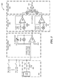
- FIG. 3 shows an exemplary implementation of a focal plane array signal path 300 for reading out the aggregated pixel data in accordance with exemplary embodiments of the invention.
- An aggregated superpixel circuit 302 includes an aggregated integration capacitor 304 for a pixel group, such as a 4x4 group of neighboring pixels. Aggregation is done in the unit cell by merging integration capacitors for groups of neighboring pixels. In general, the aggregated integration capacitor 304 should be sized to prevent saturation.
- a first switch 306 provides sample and hold functionality and a second switch 308 provides read out functionality for a charge amplifier circuit 310.
- an output line 309 is shared by many pixels in a column, e.g., 1024 pixels in a column.
- the charge amplifier circuit 310 includes a charge amplifier 312 with an adjustable gain 314 to receive a charge mode readout and provide an output signal to a sample/hold circuit 316.
- the sample/hold circuit 316 includes an odd row sample and hold 318 and an even row sample and hold 320.
- Outputs of the sample and hold circuits 318, 320 are provided to an output stage 322, which includes a multiplexer circuit 324, such as a 64-to-1 column multiplexer, to output the aggregated signal data 326.
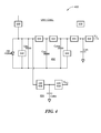
- FIG. 4 shows an exemplary pixel circuitry unit cell 400 to provide pixel-level signals for the FPA including the higher resolution imagery, lower frame rate signal path 402 and the lower resolution aggregated, higher frame rate signal path 404.
- the pixel circuit includes a photodetector PD for one row and one column of an array.
- the unit cells are connected to an associated column amplifier, such as of type shown in charge amplifier circuit 310 of FIG. 3 .
- the unit cell 400 includes an integration capacitor Cint, a sample and hold capacitor Csh, and a charge averaging capacitor Cave and a series of switches SW to control operation and sampling of the capacitors.
- a voltage sampling capacitor Cqs is also provided to implement the subframe averager low-pass filter function for the high resolution, low frame rate pixel signals.
- the charge for each pixel is integrated within each unit cell.
- the subframe averaged output Vo enhances the dynamic range of the high resolution pixel signals.
- the integration process begins as the charge converted by the photodetector PD is integrated across the integration capacitor Cint during each subframe period. It is understood that there are n subframes within one frame. At the end of a subframe period, the switches effectuate the transfer of the charge photogenerated in the photodetector PD from the integration capacitor Cint to the charge averaging capacitor Cave.
- the charge integrated across the integration capacitor Cint is passed across the sample and hold capacitor Csh. Once the charge is passed to the sample and hold capacitor Csh, the integration capacitor Cint is reset, and a new high resolution signal is built up on Cave over multiple subframes while the data on Csh is read out from the pixels to the FPA output.
- the next charge photogenerated in the photodetector PD is integrated across the integration capacitor Cint.
- the end of the subframe effectuates the transfer of the next charge photogenerated in the photodetector PD from the integration capacitor Cint to the charge averaging capacitor Cave. This continues for each subframe period as incident radiation received by the photodetector is repetitively sampled. It is noted that during the subframe periods the charge across the charge averaging capacitor Cave is not reset. As a result, charge is averaged and held on the charge averaging capacitor Cave.
- the signal on Cave is transferred to Csh and then each row and column of the FPA is readout.
- the event indicator (aggregation) circuit 404 includes a sampling switch 406 to transfer charge on a subframe basis to an event indicator integration and sample/hold capacitor Cshe.
- the event indicator sample/hold capacitor Cshe integrates the subframe charge for charge mode output to a column charge amplifier under the control of a charge readout switch 408.
- the output of the event indicator circuit 404 is normally at the subframe rate.
- the subframe and event indicator integration times are independently adjustable.
- the first ten percent of the subframe is event indicator integration and sample/hold, and the remaining ninety percent is subframe average (SFA) integration.
- the display 106 shows only the high resolution imagery for observation by a user.
- the lower resolution, higher frame rate information is processed by a computer to identify events of interest, such as pulsed light. It is understood that identifying objects of interest in a video stream is well known to one of ordinary skill in the art.
- locations generating the pulsed light detected by the computer are indicated on the display 106. In one particular embodiment, the locations of pulsed light or other detected event are passed to a weapon system.
- a computer includes a processor 502, a volatile memory 504, an output device 505, a non-volatile memory 506 (e.g., hard disk), and a graphical user interface (GUI) 508 (e.g., a mouse, a keyboard, a display, for example).
- the non-volatile memory 506 stores computer instructions 512, an operating system 516 and data 518, for example.
- the computer instructions 512 are executed by the processor 502 out of volatile memory 504 to perform all or part of the processing described above.
- An article 519 can comprise a machine-readable medium that stores executable instructions causing a machine to perform any portion of the processing described herein.
- Processing is not limited to use with the hardware and software described herein and may find applicability in any computing or processing environment and with any type of machine or set of machines that is capable of running a computer program. Processing may be implemented in hardware, software, or a combination of the two. Processing may be implemented in computer programs executed on programmable computers/machines that each includes a processor, a storage medium or other article of manufacture that is readable by the processor (including volatile and non-volatile memory and/or storage elements), at least one input device, and one or more output devices. Programs may be implemented in a high level procedural or object-oriented programming language to communicate with a computer system. However, the programs may be implemented in assembly or machine language.
- the language may be a compiled or an interpreted language and it may be deployed in any form, including as a stand-alone program or as a module, component, subroutine, or other unit suitable for use in a computing environment.
- a computer program may be deployed to be executed on one computer or on multiple computers at one site or distributed across multiple sites and interconnected by a communication network.
- a computer program may be stored on a storage medium or device (e.g., CD-ROM, hard disk, or magnetic diskette) that is readable by a general or special purpose programmable computer for configuring and operating the computer when the storage medium or device is read by the computer to perform processing.
- Exemplary embodiments of the invention provide a sensor system to use highfrequency signal samples of a subframe averager, together with aggregation of these signals for multiple neighboring pixels, and read out both SFA-processed full resolution signals and aggregated event indicator signals.
- This arrangement achieves a two-in-one sensor that simultaneously provides a conventional high-resolution moderate frame rate imaging function, as well as a lower-resolution high frame rate imaging function for detecting and classifying relatively fast transient events in a scene, such as pulsed light.
- pulsed does not require any periodicity, i.e., the pulses can be random in time and of relatively short duration. It is further understood that short duration is a relative term. For example, a muzzle flash is short with respect to a human being able to visually perceive it. However, a muzzle flash could be relatively long in other contexts.
- the frame rate can vary to detect events having particular frequencies and frequency ranges.
- the characteristics of the event can vary, such as by color, wavelength, sensor type, sensor data, patterns, and the like.
Landscapes
- Engineering & Computer Science (AREA)
- Multimedia (AREA)
- Signal Processing (AREA)
- Photometry And Measurement Of Optical Pulse Characteristics (AREA)
- Studio Devices (AREA)
- Testing, Inspecting, Measuring Of Stereoscopic Televisions And Televisions (AREA)
Applications Claiming Priority (1)
| Application Number | Priority Date | Filing Date | Title |
|---|---|---|---|
| US13/270,557 US9635287B2 (en) | 2011-10-11 | 2011-10-11 | Method and apparatus for integrated sensor to provide higher resolution, lower frame rate and lower resolution, higher frame rate imagery simultaneously |
Publications (3)
| Publication Number | Publication Date |
|---|---|
| EP2582131A2 true EP2582131A2 (fr) | 2013-04-17 |
| EP2582131A3 EP2582131A3 (fr) | 2013-10-30 |
| EP2582131B1 EP2582131B1 (fr) | 2015-12-09 |
Family
ID=47427204
Family Applications (1)
| Application Number | Title | Priority Date | Filing Date |
|---|---|---|---|
| EP12187672.6A Active EP2582131B1 (fr) | 2011-10-11 | 2012-10-08 | Procédé et appareil destinés à un capteur intégré pour fournir une résolution supérieure, une fréquence d'image inférieure, une résolution inférieure et une fréquence d'image supérieure simultanément |
Country Status (3)
| Country | Link |
|---|---|
| US (1) | US9635287B2 (fr) |
| EP (1) | EP2582131B1 (fr) |
| IL (1) | IL222280A (fr) |
Cited By (6)
| Publication number | Priority date | Publication date | Assignee | Title |
|---|---|---|---|---|
| WO2015084631A1 (fr) * | 2013-12-06 | 2015-06-11 | Raytheon Company | Plans focaux d'observation électro-optiques (eo)/infrarouges (ir) à traitement de zone d'intérêt à grande vitesse et capacité rétrospective d'expertise conduite par les événements |
| EP2911092A1 (fr) * | 2014-02-24 | 2015-08-26 | Elta Systems Ltd. | Détection de flash |
| WO2018144076A1 (fr) * | 2017-02-03 | 2018-08-09 | Raytheon Company | Détection d'événement basée sur un pixel pour suivi, indication d'incendie hostile, suppression de reflet et autres applications |
| CN108462842A (zh) * | 2018-05-14 | 2018-08-28 | 恒玄科技(上海)有限公司 | 一种高准确度、低功耗的视屏监控方法及监控系统 |
| US10520589B2 (en) | 2017-10-16 | 2019-12-31 | Sensors Unlimited, Inc. | Multimode ROIC pixel with laser range finding (LRF) capability |
| US10955551B2 (en) | 2017-10-16 | 2021-03-23 | Sensors Unlimited, Inc. | Pixel output processing circuit with laser range finding (LRF) capability |
Families Citing this family (9)
| Publication number | Priority date | Publication date | Assignee | Title |
|---|---|---|---|---|
| IL236364B (en) * | 2014-12-21 | 2019-01-31 | Elta Systems Ltd | Flash detection system and methods |
| US10012533B2 (en) * | 2016-01-15 | 2018-07-03 | Raytheon Company | Semi-active laser (SAL) receivers and methods of use thereof |
| US11288461B2 (en) | 2017-07-27 | 2022-03-29 | Bae Systems Information And Electronic Systems Integration Inc. | High voltage gain switched capacitor filter integration |
| US11436823B1 (en) * | 2019-01-21 | 2022-09-06 | Cyan Systems | High resolution fast framing infrared detection system |
| US11448483B1 (en) | 2019-04-29 | 2022-09-20 | Cyan Systems | Projectile tracking and 3D traceback method |
| US11637972B2 (en) | 2019-06-28 | 2023-04-25 | Cyan Systems | Fast framing moving target imaging system and method |
| KR20210002966A (ko) * | 2019-07-01 | 2021-01-11 | 삼성전자주식회사 | 이미지 센서 및 그것의 구동 방법 |
| US11153522B2 (en) | 2019-11-29 | 2021-10-19 | Raytheon Company | Imaging system including digital dual speed readout integrated circuit (ROIC) |
| US20260095576A1 (en) * | 2024-09-27 | 2026-04-02 | GDC Technology Limited | Systems, devices, and methods for encoding and playback of higher resolution digital cinema content |
Family Cites Families (12)
| Publication number | Priority date | Publication date | Assignee | Title |
|---|---|---|---|---|
| US5272535A (en) | 1991-06-13 | 1993-12-21 | Loral Fairchild Corporation | Image sensor with exposure control, selectable interlaced, pseudo interlaced or non-interlaced readout and video compression |
| US5808350A (en) | 1997-01-03 | 1998-09-15 | Raytheon Company | Integrated IR, visible and NIR sensor and methods of fabricating same |
| US6040568A (en) | 1998-05-06 | 2000-03-21 | Raytheon Company | Multipurpose readout integrated circuit with in cell adaptive non-uniformity correction and enhanced dynamic range |
| EP1181816A4 (fr) * | 1999-02-24 | 2006-11-02 | Dialog Semiconductor Gmbh | Procede et appareil pour sortie d'affichage foveal a resolution double |
| US6885002B1 (en) | 2001-08-31 | 2005-04-26 | Raytheon Company | IRFPA ROIC with dual TDM reset integrators and sub-frame averaging functions per unit cell |
| US6649913B1 (en) | 2002-02-26 | 2003-11-18 | Raytheon Company | Method and apparatus providing focal plane array active thermal control elements |
| US6587001B1 (en) | 2002-09-25 | 2003-07-01 | Raytheon Company | Analog load driver |
| JP2004264332A (ja) * | 2003-01-24 | 2004-09-24 | Hamamatsu Photonics Kk | 多重画像形成位置ずれ検出装置、画像濃度検出装置及び多重画像形成装置 |
| EP3620968A1 (fr) * | 2005-11-08 | 2020-03-11 | General Atomics | Appareil et procédés servant lors d'une detection de flash |
| US7593040B2 (en) | 2006-01-30 | 2009-09-22 | Omnivision Technologies, Inc. | Image anti-shake in digital cameras |
| US8681185B2 (en) * | 2009-03-05 | 2014-03-25 | Ostendo Technologies, Inc. | Multi-pixel addressing method for video display drivers |
| US8970706B2 (en) * | 2011-09-22 | 2015-03-03 | Basil Henry Scott | Dual pixel pitch imaging array with extended dynamic range |
-
2011
- 2011-10-11 US US13/270,557 patent/US9635287B2/en active Active
-
2012
- 2012-10-08 EP EP12187672.6A patent/EP2582131B1/fr active Active
- 2012-10-09 IL IL222280A patent/IL222280A/en active IP Right Grant
Non-Patent Citations (1)
| Title |
|---|
| None |
Cited By (14)
| Publication number | Priority date | Publication date | Assignee | Title |
|---|---|---|---|---|
| WO2015084631A1 (fr) * | 2013-12-06 | 2015-06-11 | Raytheon Company | Plans focaux d'observation électro-optiques (eo)/infrarouges (ir) à traitement de zone d'intérêt à grande vitesse et capacité rétrospective d'expertise conduite par les événements |
| US9386220B2 (en) | 2013-12-06 | 2016-07-05 | Raytheon Company | Electro-optical (EO)/infrared (IR) staring focal planes with high rate region of interest processing and event driven forensic look-back capability |
| EP2911092A1 (fr) * | 2014-02-24 | 2015-08-26 | Elta Systems Ltd. | Détection de flash |
| US9704058B2 (en) | 2014-02-24 | 2017-07-11 | Elta Systems Ltd. | Flash detection |
| US10410082B2 (en) | 2014-02-24 | 2019-09-10 | Elta Systems Ltd. | Flash detection |
| US10242268B2 (en) | 2017-02-03 | 2019-03-26 | Raytheon Company | Pixel-based event detection for tracking, hostile fire indication, glint suppression, and other applications |
| IL266449A (en) * | 2017-02-03 | 2019-06-30 | Raytheon Co | Pixel-based event detection for tracking, hostile fire sign, flicker suppression, and other applications |
| WO2018144076A1 (fr) * | 2017-02-03 | 2018-08-09 | Raytheon Company | Détection d'événement basée sur un pixel pour suivi, indication d'incendie hostile, suppression de reflet et autres applications |
| CN110249616A (zh) * | 2017-02-03 | 2019-09-17 | 雷神公司 | 用于跟踪、敌方火力指示、闪烁抑制以及其他应用的基于像素的事件检测 |
| US10839229B2 (en) | 2017-02-03 | 2020-11-17 | Raytheon Company | Pixel-based event detection for tracking, hostile fire indication, glint suppression, and other applications |
| CN110249616B (zh) * | 2017-02-03 | 2021-09-14 | 雷神公司 | 用于跟踪、敌方火力指示、闪烁抑制以及其他应用的基于像素的事件检测的方法、装置及系统 |
| US10520589B2 (en) | 2017-10-16 | 2019-12-31 | Sensors Unlimited, Inc. | Multimode ROIC pixel with laser range finding (LRF) capability |
| US10955551B2 (en) | 2017-10-16 | 2021-03-23 | Sensors Unlimited, Inc. | Pixel output processing circuit with laser range finding (LRF) capability |
| CN108462842A (zh) * | 2018-05-14 | 2018-08-28 | 恒玄科技(上海)有限公司 | 一种高准确度、低功耗的视屏监控方法及监控系统 |
Also Published As
| Publication number | Publication date |
|---|---|
| US9635287B2 (en) | 2017-04-25 |
| EP2582131A3 (fr) | 2013-10-30 |
| EP2582131B1 (fr) | 2015-12-09 |
| IL222280A (en) | 2017-06-29 |
| US20130088594A1 (en) | 2013-04-11 |
Similar Documents
| Publication | Publication Date | Title |
|---|---|---|
| US9635287B2 (en) | Method and apparatus for integrated sensor to provide higher resolution, lower frame rate and lower resolution, higher frame rate imagery simultaneously | |
| US11122232B2 (en) | Pixel collection circuit and optical flow sensor | |
| US12022211B1 (en) | Pixel collection circuit, optical flow sensor, and optical flow and image information collection system | |
| EP3577892B1 (fr) | Détection d'événement basée sur un pixel pour suivi, indication d'incendie hostile, suppression de reflet et autres applications | |
| US9128195B2 (en) | Increasing dynamic range for x-ray image sensor | |
| EP3388858A1 (fr) | Dispositif d'imagerie à état solide, dispositif de mesure de distance et procédé de mesure de distance | |
| WO2017081837A1 (fr) | Appareil d'imagerie par rayonnement et procédé de comptage de photons | |
| US9185314B2 (en) | Mitigating the effects of signal overload in analog front-end circuits used in image sensing systems | |
| US20200371261A1 (en) | Photon counting device and photon counting method | |
| EP1762088A2 (fr) | Dispositif d'imagerie | |
| US8729485B2 (en) | Parallel mode readout integrated circuit for X-ray image sensor | |
| JP7163416B2 (ja) | ローリングサブフレームパルスバイアスマイクロボロメータインテグレーション | |
| EP3078059B1 (fr) | Plans focaux d'observation électro-optiques (eo)/infrarouges (ir) à traitement de zone d'intérêt à grande vitesse et capacité rétrospective d'expertise conduite par les événements | |
| EP3376754B1 (fr) | Circuit d'acquisition de pixels, capteur de flux optique, et système d'acquisition d'images | |
| US20130182075A1 (en) | Geospatial and image data collection system including image sensor for capturing 3d geospatial data and 2d image data and related methods | |
| US11770627B1 (en) | Systems and methods for direct measurement of photon arrival rate | |
| Jacquot et al. | Multiple-samples-method enabling high dynamic range imaging for high frame rate CMOS image sensor by FPGA and co-processor | |
| King et al. | Athena: a 192-channel analog pulse processing and data acquisition platform | |
| US10623670B1 (en) | Simultaneous multiple well size integration | |
| KR20250168441A (ko) | 이벤트 검출 회로부, 이벤트 검출 센서, 이벤트 검출 방법 | |
| US10097775B2 (en) | Digital output binning | |
| JP2013538532A (ja) | 露光差を測定するための方法および装置 | |
| JP3023157B2 (ja) | 太陽センサの光入射位置検出装置 | |
| WO2011117162A1 (fr) | Capteur optoélectronique et procédé de détection d'attribut de lumière impactante | |
| Bonanno et al. | SPADA: An Array of SPAD Detectors for Astrophysical Applications |
Legal Events
| Date | Code | Title | Description |
|---|---|---|---|
| PUAI | Public reference made under article 153(3) epc to a published international application that has entered the european phase |
Free format text: ORIGINAL CODE: 0009012 |
|
| 17P | Request for examination filed |
Effective date: 20121108 |
|
| AK | Designated contracting states |
Kind code of ref document: A2 Designated state(s): AL AT BE BG CH CY CZ DE DK EE ES FI FR GB GR HR HU IE IS IT LI LT LU LV MC MK MT NL NO PL PT RO RS SE SI SK SM TR |
|
| AX | Request for extension of the european patent |
Extension state: BA ME |
|
| PUAL | Search report despatched |
Free format text: ORIGINAL CODE: 0009013 |
|
| AK | Designated contracting states |
Kind code of ref document: A3 Designated state(s): AL AT BE BG CH CY CZ DE DK EE ES FI FR GB GR HR HU IE IS IT LI LT LU LV MC MK MT NL NO PL PT RO RS SE SI SK SM TR |
|
| AX | Request for extension of the european patent |
Extension state: BA ME |
|
| RIC1 | Information provided on ipc code assigned before grant |
Ipc: H04N 5/343 20110101ALI20130923BHEP Ipc: H04N 5/347 20110101AFI20130923BHEP |
|
| 17Q | First examination report despatched |
Effective date: 20150122 |
|
| GRAP | Despatch of communication of intention to grant a patent |
Free format text: ORIGINAL CODE: EPIDOSNIGR1 |
|
| INTG | Intention to grant announced |
Effective date: 20150709 |
|
| GRAS | Grant fee paid |
Free format text: ORIGINAL CODE: EPIDOSNIGR3 |
|
| GRAA | (expected) grant |
Free format text: ORIGINAL CODE: 0009210 |
|
| AK | Designated contracting states |
Kind code of ref document: B1 Designated state(s): AL AT BE BG CH CY CZ DE DK EE ES FI FR GB GR HR HU IE IS IT LI LT LU LV MC MK MT NL NO PL PT RO RS SE SI SK SM TR |
|
| REG | Reference to a national code |
Ref country code: GB Ref legal event code: FG4D |
|
| REG | Reference to a national code |
Ref country code: AT Ref legal event code: REF Ref document number: 765019 Country of ref document: AT Kind code of ref document: T Effective date: 20151215 Ref country code: CH Ref legal event code: EP |
|
| REG | Reference to a national code |
Ref country code: IE Ref legal event code: FG4D |
|
| REG | Reference to a national code |
Ref country code: DE Ref legal event code: R096 Ref document number: 602012012844 Country of ref document: DE |
|
| REG | Reference to a national code |
Ref country code: LT Ref legal event code: MG4D |
|
| REG | Reference to a national code |
Ref country code: NL Ref legal event code: MP Effective date: 20151209 |
|
| PG25 | Lapsed in a contracting state [announced via postgrant information from national office to epo] |
Ref country code: ES Free format text: LAPSE BECAUSE OF FAILURE TO SUBMIT A TRANSLATION OF THE DESCRIPTION OR TO PAY THE FEE WITHIN THE PRESCRIBED TIME-LIMIT Effective date: 20151209 Ref country code: LT Free format text: LAPSE BECAUSE OF FAILURE TO SUBMIT A TRANSLATION OF THE DESCRIPTION OR TO PAY THE FEE WITHIN THE PRESCRIBED TIME-LIMIT Effective date: 20151209 Ref country code: NO Free format text: LAPSE BECAUSE OF FAILURE TO SUBMIT A TRANSLATION OF THE DESCRIPTION OR TO PAY THE FEE WITHIN THE PRESCRIBED TIME-LIMIT Effective date: 20160309 |
|
| REG | Reference to a national code |
Ref country code: AT Ref legal event code: MK05 Ref document number: 765019 Country of ref document: AT Kind code of ref document: T Effective date: 20151209 |
|
| PG25 | Lapsed in a contracting state [announced via postgrant information from national office to epo] |
Ref country code: FI Free format text: LAPSE BECAUSE OF FAILURE TO SUBMIT A TRANSLATION OF THE DESCRIPTION OR TO PAY THE FEE WITHIN THE PRESCRIBED TIME-LIMIT Effective date: 20151209 Ref country code: RS Free format text: LAPSE BECAUSE OF FAILURE TO SUBMIT A TRANSLATION OF THE DESCRIPTION OR TO PAY THE FEE WITHIN THE PRESCRIBED TIME-LIMIT Effective date: 20151209 Ref country code: NL Free format text: LAPSE BECAUSE OF FAILURE TO SUBMIT A TRANSLATION OF THE DESCRIPTION OR TO PAY THE FEE WITHIN THE PRESCRIBED TIME-LIMIT Effective date: 20151209 Ref country code: GR Free format text: LAPSE BECAUSE OF FAILURE TO SUBMIT A TRANSLATION OF THE DESCRIPTION OR TO PAY THE FEE WITHIN THE PRESCRIBED TIME-LIMIT Effective date: 20160310 Ref country code: LV Free format text: LAPSE BECAUSE OF FAILURE TO SUBMIT A TRANSLATION OF THE DESCRIPTION OR TO PAY THE FEE WITHIN THE PRESCRIBED TIME-LIMIT Effective date: 20151209 Ref country code: SE Free format text: LAPSE BECAUSE OF FAILURE TO SUBMIT A TRANSLATION OF THE DESCRIPTION OR TO PAY THE FEE WITHIN THE PRESCRIBED TIME-LIMIT Effective date: 20151209 |
|
| PG25 | Lapsed in a contracting state [announced via postgrant information from national office to epo] |
Ref country code: IS Free format text: LAPSE BECAUSE OF FAILURE TO SUBMIT A TRANSLATION OF THE DESCRIPTION OR TO PAY THE FEE WITHIN THE PRESCRIBED TIME-LIMIT Effective date: 20151209 |
|
| PG25 | Lapsed in a contracting state [announced via postgrant information from national office to epo] |
Ref country code: CZ Free format text: LAPSE BECAUSE OF FAILURE TO SUBMIT A TRANSLATION OF THE DESCRIPTION OR TO PAY THE FEE WITHIN THE PRESCRIBED TIME-LIMIT Effective date: 20151209 Ref country code: IT Free format text: LAPSE BECAUSE OF FAILURE TO SUBMIT A TRANSLATION OF THE DESCRIPTION OR TO PAY THE FEE WITHIN THE PRESCRIBED TIME-LIMIT Effective date: 20151209 |
|
| PG25 | Lapsed in a contracting state [announced via postgrant information from national office to epo] |
Ref country code: RO Free format text: LAPSE BECAUSE OF FAILURE TO SUBMIT A TRANSLATION OF THE DESCRIPTION OR TO PAY THE FEE WITHIN THE PRESCRIBED TIME-LIMIT Effective date: 20151209 Ref country code: SM Free format text: LAPSE BECAUSE OF FAILURE TO SUBMIT A TRANSLATION OF THE DESCRIPTION OR TO PAY THE FEE WITHIN THE PRESCRIBED TIME-LIMIT Effective date: 20151209 Ref country code: AT Free format text: LAPSE BECAUSE OF FAILURE TO SUBMIT A TRANSLATION OF THE DESCRIPTION OR TO PAY THE FEE WITHIN THE PRESCRIBED TIME-LIMIT Effective date: 20151209 Ref country code: IS Free format text: LAPSE BECAUSE OF FAILURE TO SUBMIT A TRANSLATION OF THE DESCRIPTION OR TO PAY THE FEE WITHIN THE PRESCRIBED TIME-LIMIT Effective date: 20160409 Ref country code: SK Free format text: LAPSE BECAUSE OF FAILURE TO SUBMIT A TRANSLATION OF THE DESCRIPTION OR TO PAY THE FEE WITHIN THE PRESCRIBED TIME-LIMIT Effective date: 20151209 Ref country code: EE Free format text: LAPSE BECAUSE OF FAILURE TO SUBMIT A TRANSLATION OF THE DESCRIPTION OR TO PAY THE FEE WITHIN THE PRESCRIBED TIME-LIMIT Effective date: 20151209 Ref country code: PT Free format text: LAPSE BECAUSE OF FAILURE TO SUBMIT A TRANSLATION OF THE DESCRIPTION OR TO PAY THE FEE WITHIN THE PRESCRIBED TIME-LIMIT Effective date: 20160411 |
|
| REG | Reference to a national code |
Ref country code: DE Ref legal event code: R097 Ref document number: 602012012844 Country of ref document: DE |
|
| REG | Reference to a national code |
Ref country code: FR Ref legal event code: PLFP Year of fee payment: 5 |
|
| PLBE | No opposition filed within time limit |
Free format text: ORIGINAL CODE: 0009261 |
|
| STAA | Information on the status of an ep patent application or granted ep patent |
Free format text: STATUS: NO OPPOSITION FILED WITHIN TIME LIMIT |
|
| PG25 | Lapsed in a contracting state [announced via postgrant information from national office to epo] |
Ref country code: DK Free format text: LAPSE BECAUSE OF FAILURE TO SUBMIT A TRANSLATION OF THE DESCRIPTION OR TO PAY THE FEE WITHIN THE PRESCRIBED TIME-LIMIT Effective date: 20151209 Ref country code: PL Free format text: LAPSE BECAUSE OF FAILURE TO SUBMIT A TRANSLATION OF THE DESCRIPTION OR TO PAY THE FEE WITHIN THE PRESCRIBED TIME-LIMIT Effective date: 20151209 |
|
| 26N | No opposition filed |
Effective date: 20160912 |
|
| PG25 | Lapsed in a contracting state [announced via postgrant information from national office to epo] |
Ref country code: SI Free format text: LAPSE BECAUSE OF FAILURE TO SUBMIT A TRANSLATION OF THE DESCRIPTION OR TO PAY THE FEE WITHIN THE PRESCRIBED TIME-LIMIT Effective date: 20151209 |
|
| PG25 | Lapsed in a contracting state [announced via postgrant information from national office to epo] |
Ref country code: BE Free format text: LAPSE BECAUSE OF FAILURE TO SUBMIT A TRANSLATION OF THE DESCRIPTION OR TO PAY THE FEE WITHIN THE PRESCRIBED TIME-LIMIT Effective date: 20151209 |
|
| REG | Reference to a national code |
Ref country code: CH Ref legal event code: PL |
|
| REG | Reference to a national code |
Ref country code: IE Ref legal event code: MM4A |
|
| PG25 | Lapsed in a contracting state [announced via postgrant information from national office to epo] |
Ref country code: CH Free format text: LAPSE BECAUSE OF NON-PAYMENT OF DUE FEES Effective date: 20161031 Ref country code: LI Free format text: LAPSE BECAUSE OF NON-PAYMENT OF DUE FEES Effective date: 20161031 |
|
| PG25 | Lapsed in a contracting state [announced via postgrant information from national office to epo] |
Ref country code: LU Free format text: LAPSE BECAUSE OF NON-PAYMENT OF DUE FEES Effective date: 20161008 |
|
| REG | Reference to a national code |
Ref country code: FR Ref legal event code: PLFP Year of fee payment: 6 |
|
| PG25 | Lapsed in a contracting state [announced via postgrant information from national office to epo] |
Ref country code: IE Free format text: LAPSE BECAUSE OF NON-PAYMENT OF DUE FEES Effective date: 20161008 |
|
| PG25 | Lapsed in a contracting state [announced via postgrant information from national office to epo] |
Ref country code: CY Free format text: LAPSE BECAUSE OF FAILURE TO SUBMIT A TRANSLATION OF THE DESCRIPTION OR TO PAY THE FEE WITHIN THE PRESCRIBED TIME-LIMIT Effective date: 20151209 Ref country code: HU Free format text: LAPSE BECAUSE OF FAILURE TO SUBMIT A TRANSLATION OF THE DESCRIPTION OR TO PAY THE FEE WITHIN THE PRESCRIBED TIME-LIMIT; INVALID AB INITIO Effective date: 20121008 |
|
| PG25 | Lapsed in a contracting state [announced via postgrant information from national office to epo] |
Ref country code: MT Free format text: LAPSE BECAUSE OF NON-PAYMENT OF DUE FEES Effective date: 20161031 Ref country code: HR Free format text: LAPSE BECAUSE OF FAILURE TO SUBMIT A TRANSLATION OF THE DESCRIPTION OR TO PAY THE FEE WITHIN THE PRESCRIBED TIME-LIMIT Effective date: 20151209 Ref country code: MC Free format text: LAPSE BECAUSE OF FAILURE TO SUBMIT A TRANSLATION OF THE DESCRIPTION OR TO PAY THE FEE WITHIN THE PRESCRIBED TIME-LIMIT Effective date: 20151209 Ref country code: TR Free format text: LAPSE BECAUSE OF FAILURE TO SUBMIT A TRANSLATION OF THE DESCRIPTION OR TO PAY THE FEE WITHIN THE PRESCRIBED TIME-LIMIT Effective date: 20151209 Ref country code: MK Free format text: LAPSE BECAUSE OF FAILURE TO SUBMIT A TRANSLATION OF THE DESCRIPTION OR TO PAY THE FEE WITHIN THE PRESCRIBED TIME-LIMIT Effective date: 20151209 |
|
| PG25 | Lapsed in a contracting state [announced via postgrant information from national office to epo] |
Ref country code: BG Free format text: LAPSE BECAUSE OF FAILURE TO SUBMIT A TRANSLATION OF THE DESCRIPTION OR TO PAY THE FEE WITHIN THE PRESCRIBED TIME-LIMIT Effective date: 20151209 |
|
| REG | Reference to a national code |
Ref country code: FR Ref legal event code: PLFP Year of fee payment: 7 |
|
| PG25 | Lapsed in a contracting state [announced via postgrant information from national office to epo] |
Ref country code: AL Free format text: LAPSE BECAUSE OF FAILURE TO SUBMIT A TRANSLATION OF THE DESCRIPTION OR TO PAY THE FEE WITHIN THE PRESCRIBED TIME-LIMIT Effective date: 20151209 |
|
| REG | Reference to a national code |
Ref country code: DE Ref legal event code: R079 Ref document number: 602012012844 Country of ref document: DE Free format text: PREVIOUS MAIN CLASS: H04N0005347000 Ipc: H04N0025460000 |
|
| P01 | Opt-out of the competence of the unified patent court (upc) registered |
Effective date: 20230530 |
|
| PGFP | Annual fee paid to national office [announced via postgrant information from national office to epo] |
Ref country code: GB Payment date: 20250923 Year of fee payment: 14 |
|
| PGFP | Annual fee paid to national office [announced via postgrant information from national office to epo] |
Ref country code: FR Payment date: 20250924 Year of fee payment: 14 |
|
| PGFP | Annual fee paid to national office [announced via postgrant information from national office to epo] |
Ref country code: DE Payment date: 20250923 Year of fee payment: 14 |