EP2583833B1 - Imprimante à jet d'encre comprenant une séquence de démarrage de gicleur - Google Patents
Imprimante à jet d'encre comprenant une séquence de démarrage de gicleur Download PDFInfo
- Publication number
- EP2583833B1 EP2583833B1 EP13151348.3A EP13151348A EP2583833B1 EP 2583833 B1 EP2583833 B1 EP 2583833B1 EP 13151348 A EP13151348 A EP 13151348A EP 2583833 B1 EP2583833 B1 EP 2583833B1
- Authority
- EP
- European Patent Office
- Prior art keywords
- nozzles
- row
- printhead
- nozzle
- span
- Prior art date
- Legal status (The legal status is an assumption and is not a legal conclusion. Google has not performed a legal analysis and makes no representation as to the accuracy of the status listed.)
- Not-in-force
Links
- 238000010304 firing Methods 0.000 title claims description 84
- 238000007639 printing Methods 0.000 claims description 30
- 239000012530 fluid Substances 0.000 claims description 13
- 238000012423 maintenance Methods 0.000 claims description 6
- 230000004044 response Effects 0.000 claims description 5
- 239000000976 ink Substances 0.000 description 66
- 238000012360 testing method Methods 0.000 description 19
- 238000000034 method Methods 0.000 description 8
- 239000011295 pitch Substances 0.000 description 7
- 239000000758 substrate Substances 0.000 description 7
- 230000002950 deficient Effects 0.000 description 6
- 230000003111 delayed effect Effects 0.000 description 6
- 230000001627 detrimental effect Effects 0.000 description 6
- 230000006911 nucleation Effects 0.000 description 6
- 238000010899 nucleation Methods 0.000 description 6
- 238000004519 manufacturing process Methods 0.000 description 5
- 230000008859 change Effects 0.000 description 4
- 238000013461 design Methods 0.000 description 4
- 239000000523 sample Substances 0.000 description 4
- 230000001934 delay Effects 0.000 description 3
- 230000008569 process Effects 0.000 description 3
- 238000000926 separation method Methods 0.000 description 3
- XUIMIQQOPSSXEZ-UHFFFAOYSA-N Silicon Chemical compound [Si] XUIMIQQOPSSXEZ-UHFFFAOYSA-N 0.000 description 2
- 239000003086 colorant Substances 0.000 description 2
- 238000010276 construction Methods 0.000 description 2
- 230000001186 cumulative effect Effects 0.000 description 2
- 238000001514 detection method Methods 0.000 description 2
- 230000000694 effects Effects 0.000 description 2
- 238000009434 installation Methods 0.000 description 2
- 230000000630 rising effect Effects 0.000 description 2
- 230000011664 signaling Effects 0.000 description 2
- 229910052710 silicon Inorganic materials 0.000 description 2
- 239000010703 silicon Substances 0.000 description 2
- 102100030796 E3 ubiquitin-protein ligase rififylin Human genes 0.000 description 1
- 101710128004 E3 ubiquitin-protein ligase rififylin Proteins 0.000 description 1
- 238000006424 Flood reaction Methods 0.000 description 1
- 241001481828 Glyptocephalus cynoglossus Species 0.000 description 1
- 230000003213 activating effect Effects 0.000 description 1
- 230000004913 activation Effects 0.000 description 1
- 239000000853 adhesive Substances 0.000 description 1
- 230000001070 adhesive effect Effects 0.000 description 1
- 238000003491 array Methods 0.000 description 1
- 230000002457 bidirectional effect Effects 0.000 description 1
- 238000004891 communication Methods 0.000 description 1
- 230000001143 conditioned effect Effects 0.000 description 1
- 230000003750 conditioning effect Effects 0.000 description 1
- 230000001419 dependent effect Effects 0.000 description 1
- 238000009792 diffusion process Methods 0.000 description 1
- 238000006073 displacement reaction Methods 0.000 description 1
- 238000009826 distribution Methods 0.000 description 1
- 239000003814 drug Substances 0.000 description 1
- 238000005868 electrolysis reaction Methods 0.000 description 1
- 238000005265 energy consumption Methods 0.000 description 1
- 238000003384 imaging method Methods 0.000 description 1
- 230000002452 interceptive effect Effects 0.000 description 1
- 238000012804 iterative process Methods 0.000 description 1
- 230000004048 modification Effects 0.000 description 1
- 238000012986 modification Methods 0.000 description 1
- 238000010943 off-gassing Methods 0.000 description 1
- 230000000737 periodic effect Effects 0.000 description 1
- 239000004065 semiconductor Substances 0.000 description 1
- 238000004904 shortening Methods 0.000 description 1
- 239000007787 solid Substances 0.000 description 1
- 230000007704 transition Effects 0.000 description 1
- 238000010792 warming Methods 0.000 description 1
- XLYOFNOQVPJJNP-UHFFFAOYSA-N water Substances O XLYOFNOQVPJJNP-UHFFFAOYSA-N 0.000 description 1
Images





Classifications
-
- B—PERFORMING OPERATIONS; TRANSPORTING
- B41—PRINTING; LINING MACHINES; TYPEWRITERS; STAMPS
- B41J—TYPEWRITERS; SELECTIVE PRINTING MECHANISMS, i.e. MECHANISMS PRINTING OTHERWISE THAN FROM A FORME; CORRECTION OF TYPOGRAPHICAL ERRORS
- B41J2/00—Typewriters or selective printing mechanisms characterised by the printing or marking process for which they are designed
- B41J2/315—Typewriters or selective printing mechanisms characterised by the printing or marking process for which they are designed characterised by selective application of heat to a heat sensitive printing or impression-transfer material
- B41J2/32—Typewriters or selective printing mechanisms characterised by the printing or marking process for which they are designed characterised by selective application of heat to a heat sensitive printing or impression-transfer material using thermal heads
- B41J2/345—Typewriters or selective printing mechanisms characterised by the printing or marking process for which they are designed characterised by selective application of heat to a heat sensitive printing or impression-transfer material using thermal heads characterised by the arrangement of resistors or conductors
-
- B—PERFORMING OPERATIONS; TRANSPORTING
- B41—PRINTING; LINING MACHINES; TYPEWRITERS; STAMPS
- B41J—TYPEWRITERS; SELECTIVE PRINTING MECHANISMS, i.e. MECHANISMS PRINTING OTHERWISE THAN FROM A FORME; CORRECTION OF TYPOGRAPHICAL ERRORS
- B41J2/00—Typewriters or selective printing mechanisms characterised by the printing or marking process for which they are designed
- B41J2/005—Typewriters or selective printing mechanisms characterised by the printing or marking process for which they are designed characterised by bringing liquid or particles selectively into contact with a printing material
- B41J2/01—Ink jet
- B41J2/135—Nozzles
- B41J2/145—Arrangement thereof
- B41J2/155—Arrangement thereof for line printing
-
- B—PERFORMING OPERATIONS; TRANSPORTING
- B41—PRINTING; LINING MACHINES; TYPEWRITERS; STAMPS
- B41J—TYPEWRITERS; SELECTIVE PRINTING MECHANISMS, i.e. MECHANISMS PRINTING OTHERWISE THAN FROM A FORME; CORRECTION OF TYPOGRAPHICAL ERRORS
- B41J2/00—Typewriters or selective printing mechanisms characterised by the printing or marking process for which they are designed
- B41J2/005—Typewriters or selective printing mechanisms characterised by the printing or marking process for which they are designed characterised by bringing liquid or particles selectively into contact with a printing material
- B41J2/01—Ink jet
- B41J2/015—Ink jet characterised by the jet generation process
- B41J2/04—Ink jet characterised by the jet generation process generating single droplets or particles on demand
- B41J2/045—Ink jet characterised by the jet generation process generating single droplets or particles on demand by pressure, e.g. electromechanical transducers
- B41J2/04501—Control methods or devices therefor, e.g. driver circuits, control circuits
- B41J2/0454—Control methods or devices therefor, e.g. driver circuits, control circuits involving calculation of temperature
-
- B—PERFORMING OPERATIONS; TRANSPORTING
- B41—PRINTING; LINING MACHINES; TYPEWRITERS; STAMPS
- B41J—TYPEWRITERS; SELECTIVE PRINTING MECHANISMS, i.e. MECHANISMS PRINTING OTHERWISE THAN FROM A FORME; CORRECTION OF TYPOGRAPHICAL ERRORS
- B41J2/00—Typewriters or selective printing mechanisms characterised by the printing or marking process for which they are designed
- B41J2/005—Typewriters or selective printing mechanisms characterised by the printing or marking process for which they are designed characterised by bringing liquid or particles selectively into contact with a printing material
- B41J2/01—Ink jet
- B41J2/015—Ink jet characterised by the jet generation process
- B41J2/04—Ink jet characterised by the jet generation process generating single droplets or particles on demand
- B41J2/045—Ink jet characterised by the jet generation process generating single droplets or particles on demand by pressure, e.g. electromechanical transducers
- B41J2/04501—Control methods or devices therefor, e.g. driver circuits, control circuits
- B41J2/04541—Specific driving circuit
-
- B—PERFORMING OPERATIONS; TRANSPORTING
- B41—PRINTING; LINING MACHINES; TYPEWRITERS; STAMPS
- B41J—TYPEWRITERS; SELECTIVE PRINTING MECHANISMS, i.e. MECHANISMS PRINTING OTHERWISE THAN FROM A FORME; CORRECTION OF TYPOGRAPHICAL ERRORS
- B41J2/00—Typewriters or selective printing mechanisms characterised by the printing or marking process for which they are designed
- B41J2/005—Typewriters or selective printing mechanisms characterised by the printing or marking process for which they are designed characterised by bringing liquid or particles selectively into contact with a printing material
- B41J2/01—Ink jet
- B41J2/015—Ink jet characterised by the jet generation process
- B41J2/04—Ink jet characterised by the jet generation process generating single droplets or particles on demand
- B41J2/045—Ink jet characterised by the jet generation process generating single droplets or particles on demand by pressure, e.g. electromechanical transducers
- B41J2/04501—Control methods or devices therefor, e.g. driver circuits, control circuits
- B41J2/04565—Control methods or devices therefor, e.g. driver circuits, control circuits detecting heater resistance
-
- B—PERFORMING OPERATIONS; TRANSPORTING
- B41—PRINTING; LINING MACHINES; TYPEWRITERS; STAMPS
- B41J—TYPEWRITERS; SELECTIVE PRINTING MECHANISMS, i.e. MECHANISMS PRINTING OTHERWISE THAN FROM A FORME; CORRECTION OF TYPOGRAPHICAL ERRORS
- B41J2/00—Typewriters or selective printing mechanisms characterised by the printing or marking process for which they are designed
- B41J2/005—Typewriters or selective printing mechanisms characterised by the printing or marking process for which they are designed characterised by bringing liquid or particles selectively into contact with a printing material
- B41J2/01—Ink jet
- B41J2/015—Ink jet characterised by the jet generation process
- B41J2/04—Ink jet characterised by the jet generation process generating single droplets or particles on demand
- B41J2/045—Ink jet characterised by the jet generation process generating single droplets or particles on demand by pressure, e.g. electromechanical transducers
- B41J2/04501—Control methods or devices therefor, e.g. driver circuits, control circuits
- B41J2/04596—Non-ejecting pulses
-
- B—PERFORMING OPERATIONS; TRANSPORTING
- B41—PRINTING; LINING MACHINES; TYPEWRITERS; STAMPS
- B41J—TYPEWRITERS; SELECTIVE PRINTING MECHANISMS, i.e. MECHANISMS PRINTING OTHERWISE THAN FROM A FORME; CORRECTION OF TYPOGRAPHICAL ERRORS
- B41J2/00—Typewriters or selective printing mechanisms characterised by the printing or marking process for which they are designed
- B41J2/005—Typewriters or selective printing mechanisms characterised by the printing or marking process for which they are designed characterised by bringing liquid or particles selectively into contact with a printing material
- B41J2/01—Ink jet
- B41J2/21—Ink jet for multi-colour printing
- B41J2/2132—Print quality control characterised by dot disposition, e.g. for reducing white stripes or banding
- B41J2/2142—Detection of malfunctioning nozzles
-
- B—PERFORMING OPERATIONS; TRANSPORTING
- B41—PRINTING; LINING MACHINES; TYPEWRITERS; STAMPS
- B41J—TYPEWRITERS; SELECTIVE PRINTING MECHANISMS, i.e. MECHANISMS PRINTING OTHERWISE THAN FROM A FORME; CORRECTION OF TYPOGRAPHICAL ERRORS
- B41J2/00—Typewriters or selective printing mechanisms characterised by the printing or marking process for which they are designed
- B41J2/005—Typewriters or selective printing mechanisms characterised by the printing or marking process for which they are designed characterised by bringing liquid or particles selectively into contact with a printing material
- B41J2/01—Ink jet
- B41J2/21—Ink jet for multi-colour printing
- B41J2/2132—Print quality control characterised by dot disposition, e.g. for reducing white stripes or banding
- B41J2/2146—Print quality control characterised by dot disposition, e.g. for reducing white stripes or banding for line print heads
-
- B—PERFORMING OPERATIONS; TRANSPORTING
- B41—PRINTING; LINING MACHINES; TYPEWRITERS; STAMPS
- B41J—TYPEWRITERS; SELECTIVE PRINTING MECHANISMS, i.e. MECHANISMS PRINTING OTHERWISE THAN FROM A FORME; CORRECTION OF TYPOGRAPHICAL ERRORS
- B41J2/00—Typewriters or selective printing mechanisms characterised by the printing or marking process for which they are designed
- B41J2/315—Typewriters or selective printing mechanisms characterised by the printing or marking process for which they are designed characterised by selective application of heat to a heat sensitive printing or impression-transfer material
- B41J2/32—Typewriters or selective printing mechanisms characterised by the printing or marking process for which they are designed characterised by selective application of heat to a heat sensitive printing or impression-transfer material using thermal heads
-
- B—PERFORMING OPERATIONS; TRANSPORTING
- B41—PRINTING; LINING MACHINES; TYPEWRITERS; STAMPS
- B41J—TYPEWRITERS; SELECTIVE PRINTING MECHANISMS, i.e. MECHANISMS PRINTING OTHERWISE THAN FROM A FORME; CORRECTION OF TYPOGRAPHICAL ERRORS
- B41J2/00—Typewriters or selective printing mechanisms characterised by the printing or marking process for which they are designed
- B41J2/315—Typewriters or selective printing mechanisms characterised by the printing or marking process for which they are designed characterised by selective application of heat to a heat sensitive printing or impression-transfer material
- B41J2/32—Typewriters or selective printing mechanisms characterised by the printing or marking process for which they are designed characterised by selective application of heat to a heat sensitive printing or impression-transfer material using thermal heads
- B41J2/35—Typewriters or selective printing mechanisms characterised by the printing or marking process for which they are designed characterised by selective application of heat to a heat sensitive printing or impression-transfer material using thermal heads providing current or voltage to the thermal head
-
- B—PERFORMING OPERATIONS; TRANSPORTING
- B41—PRINTING; LINING MACHINES; TYPEWRITERS; STAMPS
- B41J—TYPEWRITERS; SELECTIVE PRINTING MECHANISMS, i.e. MECHANISMS PRINTING OTHERWISE THAN FROM A FORME; CORRECTION OF TYPOGRAPHICAL ERRORS
- B41J2/00—Typewriters or selective printing mechanisms characterised by the printing or marking process for which they are designed
- B41J2/315—Typewriters or selective printing mechanisms characterised by the printing or marking process for which they are designed characterised by selective application of heat to a heat sensitive printing or impression-transfer material
- B41J2/32—Typewriters or selective printing mechanisms characterised by the printing or marking process for which they are designed characterised by selective application of heat to a heat sensitive printing or impression-transfer material using thermal heads
- B41J2/35—Typewriters or selective printing mechanisms characterised by the printing or marking process for which they are designed characterised by selective application of heat to a heat sensitive printing or impression-transfer material using thermal heads providing current or voltage to the thermal head
- B41J2/355—Control circuits for heating-element selection
-
- B—PERFORMING OPERATIONS; TRANSPORTING
- B41—PRINTING; LINING MACHINES; TYPEWRITERS; STAMPS
- B41J—TYPEWRITERS; SELECTIVE PRINTING MECHANISMS, i.e. MECHANISMS PRINTING OTHERWISE THAN FROM A FORME; CORRECTION OF TYPOGRAPHICAL ERRORS
- B41J2/00—Typewriters or selective printing mechanisms characterised by the printing or marking process for which they are designed
- B41J2/315—Typewriters or selective printing mechanisms characterised by the printing or marking process for which they are designed characterised by selective application of heat to a heat sensitive printing or impression-transfer material
- B41J2/32—Typewriters or selective printing mechanisms characterised by the printing or marking process for which they are designed characterised by selective application of heat to a heat sensitive printing or impression-transfer material using thermal heads
- B41J2/35—Typewriters or selective printing mechanisms characterised by the printing or marking process for which they are designed characterised by selective application of heat to a heat sensitive printing or impression-transfer material using thermal heads providing current or voltage to the thermal head
- B41J2/355—Control circuits for heating-element selection
- B41J2/3553—Heater resistance determination
-
- B—PERFORMING OPERATIONS; TRANSPORTING
- B41—PRINTING; LINING MACHINES; TYPEWRITERS; STAMPS
- B41J—TYPEWRITERS; SELECTIVE PRINTING MECHANISMS, i.e. MECHANISMS PRINTING OTHERWISE THAN FROM A FORME; CORRECTION OF TYPOGRAPHICAL ERRORS
- B41J2/00—Typewriters or selective printing mechanisms characterised by the printing or marking process for which they are designed
- B41J2/315—Typewriters or selective printing mechanisms characterised by the printing or marking process for which they are designed characterised by selective application of heat to a heat sensitive printing or impression-transfer material
- B41J2/32—Typewriters or selective printing mechanisms characterised by the printing or marking process for which they are designed characterised by selective application of heat to a heat sensitive printing or impression-transfer material using thermal heads
- B41J2/35—Typewriters or selective printing mechanisms characterised by the printing or marking process for which they are designed characterised by selective application of heat to a heat sensitive printing or impression-transfer material using thermal heads providing current or voltage to the thermal head
- B41J2/355—Control circuits for heating-element selection
- B41J2/36—Print density control
- B41J2/365—Print density control by compensation for variation in temperature
Definitions
- the present invention relates to the field of inkjet printers.
- the invention relates to inkjet printers that have printheads with a number of separate printhead integrated circuits (IC's) defining the nozzles that eject the ink or other printing fluid.
- IC's printhead integrated circuits
- Inkjet printers eject drops of ink through an array of nozzles to effect printing on a media substrate.
- the nozzles are typically formed on a silicon wafer substrate using semiconductor fabrication techniques.
- Each nozzle is a MEMS (micro electro-mechanical systems) device driven by associated drive circuitry formed on the same silicon wafer substrate.
- the MEMS nozzle devices and associated drive circuitry formed on a single nozzle is commonly referred to as a printhead integrated circuit (IC).
- Fabrication of the MEMS nozzle structures on wafer substrates will invariably result in some detective nozzles.
- These 'dead nozzles' can be located using a wafer probe immediately after fabrication. Knowing the location of the dead nozzles, the print engine controller (PEC) can be programmed with a dead nozzle map. This is used to compensate for the dead nozzles with techniques such as nozzle redundancy (the printhead IC is has more nozzles than necessary and uses the 'spare' nozzles to print the dots normally assign to the dead nozzles).
- nozzles also fail during the operational life of the printhead. It is not possible to locate these nozzles using a wafer probe once they have been mounted to the printhead assembly and installed in the printer. Over time, the number of dead nozzles increases and as the PEC is not aware of them, there is no attempt to compensate for them. This eventually causes visible artifacts that are detrimental to the print quality.
- US 2006/092222 relates to a printhead module including at least one row that comprises a plurality of sets of n adjacent nozzles, each of the nozzles being configured to expel ink in response to a fire signal, such that, for each set of nozzles, a fire signal is provided in accordance with the sequence: [nozzle position 1, nozzle position n, nozzle position 2, nozzle position (n-1), ... , nozzle position x], wherein nozzle position x is at or adjacent the centre of the set of nozzle.
- the present invention provides an inkjet printer comprising:
- the invention sets the nozzle firing sequence in each row such that the nozzles fire in staggered groups, the nozzles within each group can be selected so that they are not too close to a simultaneously fired nozzle, or a nozzle that is fired immediately afterwards. Staging the nozzle firings avoids the high current required for firing the whole row simultaneously. Maintaining a minimum spacing between simultaneously fired nozzles and the nozzles fired immediately after them avoids the detrimental effects of fluidic cross talk and aerodynamic interference.
- the print data is unlikely to require every nozzle in a row to fire in the same firing sequence.
- the invention enables every nozzle to fire at a certain time within the firing sequence, regardless of whether it does fire a drop. Therefore, the spacing between simultaneously firing nozzles, or sequentially firing nozzles, will often be more than the predetermined minimum spacing, but this is not detrimental to the print quality.
- the invention is concerned with ensuring the spacing between two potentially interfering drops is never less than the predetermined minimum.
- the row is divided into spans having only one nozzle from every group so that the number of spans across the row equals the number of groups of nozzles.
- the predetermined minimum number of nozzles between sequentially enabled nozzles is a uniform shift along each span in a uniform direction, the shift being a number of nozzles that is an integer greater than one and not a factor of the number of nozzles in the span, such that, the successively enabled nozzles in each span progress toward one end of the span until there are insufficient nozzles left at the end to fill the shift, in which case, the shift is completed with nozzles at the opposite end of the span so that all the nozzles in the span are enabled once during the firing sequence.
- the shift is the number of nozzles that is the nearest integer to the square root of the span, that is not a factor (i.e. the span can not be divisible by the shift without a remainder). The Applicant has found that this provides a maximum spacing in time and space for ejected drops.
- the row is divided into spans having only one nozzle from every group so that the number of spans across the row equals the number of groups of nozzles.
- the predetermined minimum number of nozzles between sequentially enabled nozzles is a uniform shift along each span in a uniform direction, the shift being a number of nozzles that is an integer greater than one and not a factor of the number of nozzles in the span, such that, the successively enabled nozzles in each span progress toward one end of the span until there are insufficient nozzles left at the end to fill the shift, in which case, the shift is completed with nozzles at the opposite end of the span so that all the nozzles in the span are enabled once during the firing sequence.
- the shift is the number of nozzles that is the nearest integer to the square root of the span, that is not a factor.
- the present invention provides an inkjet printer further comprising a plurality of temperature sensors positioned along the array of nozzles such that the drive circuitry adjusts the drive pulses in response to the temperature sensor outputs.
- each of the plurality of temperature sensors is activated sequentially for a period of time during the print job.
- the plurality of temperatures sensors are divided into two or more groups, each group being activated for a sensing period in accordance with a predetermined repeating sequence for the duration of a print job.
- each of the plurality of temperature sensors is configured to sense the temperature a corresponding region of the array such that the drive pulse for the nozzles in one region can differs from the drive pulse for the nozzles in another region.
- every second temperature sensor in the plurality of temperature sensors is de-activated such that the drive circuitry adjusts the drive pulse profile for the region corresponding to each activated temperature sensor and applies the same adjustment to the adjacent region where the temperature sensor is de-activated.
- the drive circuitry is programmed with a series of temperature thresholds defining a set of temperature zones, each of the zones having a different pulse profile for the drive pulses sent to the nozzles in the region currently operating in that temperature zone.
- the pulse profile for each temperature zone differs in its duration.
- the drive circuitry sets the pulse duration to zero if the temperature sensor indicates that region is operating at a temperature above the highest of the temperature thresholds.
- the drive circuitry sets the duration of the pulse profile to a sub ejection value for any of the nozzles in the row that are not to eject a drop during that firing sequence.
- the Applicant has developed a range of printhead devices that use a series of printhead integrated circuits (ICs) that link together to form a pagewidth printhead.
- the printheads IC's can be assembled into printheads used in applications ranging from wide format printing to cameras and cellphones with inbuilt printers.
- One of the more recent printhead IC's developed by the Applicant is referred to internally as wide range of printing applications.
- the Applicant refers to these printhead IC's as 'Udon' and the various aspects of the invention will be described with particular reference to these printhead IC's. However, it will be appreciated that this is purely for the purposes of illustration and in no way limiting to the scope and application of the invention.
- the Udon printhead IC is designed to work with other Udon ICs to make a linking printhead.
- the Applicant has developed a range of linking printheads in which a series of the printhead IC's are mounted end-to-end on a support member to form a pagewidth printhead.
- the support member mounts the printhead IC's in the printer and also distributes ink to the individual IC's.
- An examples of this type of printhead is described in USSN 11/293,820 , the disclosure of which is incorporated herein by cross reference.
- any reference to the term 'ink' is to be interpreted as any printing fluid unless it is clear from the context that it is only a colorant for imaging print media.
- the printhead IC's can equally eject invisible inks, adhesives, medicaments or other functionalized fluids.
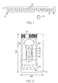
- Figure 1 shows a sketch of a pagewidth printhead 10 with the series ofUdon printheads ICs 12 mounted to a support member 14,
- the angled sides 16 allow the nozzles from one of the IC's 12 overlap with those of an adjacent IC in the paper feed direction 18. Overlapping the nozzles in each IC 12 provides continuous printing across the junction between two IC's. This avoids any 'banding' in the resulting print. Linking individual printhead IC's in this manner allows printheads of any desired length to be made by simply using different numbers of IC's.
- the printhead IC's 12 are integrated CMOS and MEMS 'chips'.
- Figure 3 shows the configuration of MEMS nozzles 20 on the ink ejection side of the printhead IC 12.
- the nozzles 20 are arranged into rows 26 and columns 24 to form a parallelogram array 22 with 'kinked' or inclined portion 28.
- the columns 24 are not aligned with the paper feed direction 18 because the sides of the array 22 are angled approximately 45° for the purposes of linking with adjacent IC's.
- the columns 24 follow this incline.
- the rows 26 are perpendicular to the paper feed direction except for a sloped section 28 inclined towards a 'drop triangle' 30 which has the nozzles 20 that overlap the adjacent pnnthead IC. This is discussed in more detail below.
- Figure 2 shows the elements of a single MEMS nozzle device 20 or 'unit cell'.
- the construction of the unit cell 20 is discussed in detail in USSN 11/246,687 , the contents of which is incorporated herein by cross reference.
- Figure 2 shows the unit cell as if the nozzle plate (the outer surface of the printhead) were transparent to expose the interior features.
- the nozzle 32 is the ejection aperture through which the ink is ejected.
- the heater 34 is positioned in the nozzle chamber 36 to generate a vapour bubble that ejects a drop of ink through the nozzle 32.
- the U-shaped sidewall 38 defines the edges of the chamber 36.
- the CMOS layer defines the drive circuitry and has a drive FET 40 for the heater 34 and logic 46 for pulse timing and profiling. This is discussed in more detail below.
- Ink is supplied to the unit cells 20 from channels in the opposite side of the wafer substrate of the printhead IC. These are described below with reference to Figure 5C .
- the channels in the 'back side' of the printhead IC 12 are in fluid communication with the unit cells 20 on the front side via deep etched conduits (not shown) through the CMOS layer.
- Each IC 12 contains ten rows 26 of nozzles 32. As shown in Figure 4 , there are two adjacent rows 26 for each color to allow up to five separate types of ink. Each pair of rows 26 shares a common ink supply channel in the back side of the wafer substrate.
- the distance between printed dots needs to be 15,875 ⁇ m: This is referred to as the dot pitch ( DP ).
- the unit cell 20 has a rectangular footprint that is 2 DP wide by 5 DP long.
- the rows 26 are offset from eachother relative to the feed direction 18 of the paper 48 as best shown in Figure 4 .
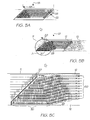
- Figure 5A shows the parallelogram that the nozzle forms by offsetting each subsequent row 26 by 5 DP.
- the parallelogram 50 does not allow the array 22 to link with those of adjacent printhead IC's. To maintain a constant dot pitch between the edge nozzles of one printhead IC and the opposing edge nozzles of the adjacent IC, the parallelogram 50 needs to be slightly distorted.
- Figure 5B shows the distortion used by the Udon design.
- a portion 30 of the array 22 is displaced or 'dropped' relative to the rest of the array with respect to the paper feed direction 18.
- the Applicant refers to this portion as the drop triangle 30.
- the unit cells 20 on the outer edge of the drop triangle 30 are directly adjacent the unit cells 20 at the edge of the adjacent printhead IC 11 in terms of their dot pitch. In this way, the separate nozzle arrays link together as if they were a single continuous array.
- the 'drop' of the drop triangle 30 is 10 DP. Dots printed by the nozzles in the triangle 30 are delayed by ten 'line times' (the line time is the time taken to print one line from the printhead IC, that is fire all ten rows in accordance with the print data at that point in the print job) to match the triangle offset. There is a transition zone 28 between the drop triangle 30 and the rest of the array 22. In this zone the rows 26 'droop' towards the drop triangle 30.
- Nine pairs of unit cells 20 sequentially drop by one line time (1 DP , 1 row time) at a time to gradually bridge the gap between dropped and normal nozzles.
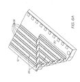
- the droop zone is purely for linking and not necessary from a printing point of view. As shown in Figure 6A , the rows 26 could simply terminate 10 DP above the corresponding row in the drop triangle 30. However, this creates a sharp corner in the ink supply channels 50 in the back of the IC 12 (see Figure 6B ). The sharp change of direction in the ink flow is problematic because outgassing bubbles can become lodged and difficult to remove from stagnation areas 54 at the corners 52.
- Figure 5C shows the configuration of the ink supply channels 50 in the back of an Udon printhead IC 12. It can be seen that the droop zone 28 keeps the ink supply channels 50 less angled and therefore free of flow stagnation areas.
- the Udon printhead IC can operate in different modes depending on the print engine controller (PEC) from which it is receiving its print data. Specifically, Udon runs in two distinct modes—SoPEC mode and MoPEC mode. SoPEC is the PEC that the Applicant uses in its SOHO (small office, home office) printers, and MoPEC is the PEC used in its mobile telecommunications (e.g. cell phone or PDA) printers. Udon does not use any type of adaptor or intermediate interface to connect to differing PEC's. Instead, Udon determines the correct operating mode (SoPEC or MoPEC) when it powers up. In each mode, the contacts on each of the printhead IC's assume different functions.
- SoPEC print engine controller
- FIG. 7 is a schematic representation of the connection of the Udon IC's 12 to a SoPEC 56.
- Each of the printhead IC's 12 has a clock input 60, a data input 58, a reset pin 62 and a data out pin 64.
- the clock and data inputs are each 2 LVDS (low voltage differential signalling) receivers with no termination.
- the reset pin 62 is a 3.3V Schmitt trigger that puts all control registers into a known state and disables printing. Nozzle firing is disabled combinatorially and three consecutive clocked samples are required to reset the registers.
- the data output pin 64 is a general purpose output but is usually used to read register values back from the printhead IC 12 to the SoPEC 56.
- the interface between SoPEC 56 and the printhead 10 has six connections.
- Figure 8 shows the connection between a MoPEC 66 and the printhead IC's 12 of a printhead 10 installed in a mobile device. Some of the same connection pins are used when the IC operates in the MoPEC mode. However, as the MoPEC printheads 10 will be physically smaller (only three chips wide for printing onto business card sized media) and more frequently replaced by the user, it is necessary to simplify the interface between the MoPEC and the printhead as much as possible. This reduces the scope for incorrect installation and enhances the intuitive usability of the mobile device.
- the address carry in (ACI) 70 is the positive pin of the LVDS pair of clock input 60 in the SoPEC mode.
- the first printhead IC 12 in the series has the ACI 70 set to ground 68 for addressing purposes described further below.
- the negative pin 60 is grounded to hold it to '0' voltage.
- the data out pin 64 connects directly to the ACI 70 of the adjacent printhead IC 12. All the IC's 12 are daisy-chained together in this manner with the last printhead IC 12 in the series having the data out 64 connected back to the MoPEC 66.
- the reset pin 62 remains unconnected and the negative pin 72 of the data LVDS pair is grounded.
- the data and clock are inputted through a single connectionusing the self-clocking data signal discussed below.
- the daisy-chained connection of the IC's 12 and the self clocking data input 58 reduce the number of connections between MoPEC and the printhead to just two. This simplifiers the printhead cartridge replacement process for the user and reduces the chance of incorrect installation.
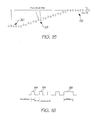
- the combined clock and data 58 is a pulse width modulated signal as shown in Figure 9 .
- the signal 74 shows one clock period and a '0' bit and the signal 76 shows one clock period and a '1' bit.
- "The Udon IC's 12 (when in MoPEC mode) takes its clock from every rising edge 78 as the signal switches from low to high (0 to 1). Accordingly, the signal has a rising edge 78 at every period.
- a '0' bit drops the signal back to '0' at 1/3 of the clock period.
- a '1' bit drops the signal to '0' at 2/3 of the clock period.
- the IC looks to the state of the signal at the mid point 80 of the period to read the '0' or the '1' bit
- Each of the printhead IC's 12 are given a write address when connected to the MoPEC 66. To do this using a two wire connection between the PEC and the printhead requires an iterative process of broadcast addressing to each device individually. Udon achieves this by daisy-chaining the data output or one IC to the address carry in of the next IC. The default or reset value at the data output 64 is high or '1'. Therefore every printhead IC 12 has a '1' address except the first printhead IC 12 which has its address pulled to '0' by its connection to ground 68. To give the IC's 12 unique write addresses, the MoPEC 66 sends a broadcast command to all devices with a '0' address.
- the only IC with a '0' address re-writes its write address to a unique address specified by MoPEC and sets its data out 64 to '0'. That in turn pulls the ACI 70 of the second IC 12 in the series to '0' so that when MoPEC again sends a broadcast command to write address '0' so that the second IC, and only the second IC, rewrites its address to a new and unique address, as well as setting its data output to '0',
- the process repeats until all the printheads IC's 12 have mutually unique write addresses and the last IC sends a '0' back to MoPEC 66.
- the interface need only have a connection for a combined data and clock 'multi-dropped' (connected in parallel) to all devices and a data out from the IC's back to MoPEC.
- a simplified electrical interface between the PEC and printhead cartridge enhances the ease and convenience of cartridge replacement.
- Udon printhead IC's 12 have a power on reset (FOR) circuit.
- FOR power on reset
- the POR circuit is implemented as a bidirectional reset pin 62 (see Figure 7 ).
- the POR circuit always drives out the reset pin 62, and the IC listens to the reset pin input side. This allows SoPEC 56 to overdrive reset when required.
- the Udon printhead IC 12 switches from mode to mode and suppresses fire commands until it determines the type of PEC to which it is connected. Once it selects the correct operating mode for the PEC, it will not try to align with another PEC type again until a software reset or power down/power up cycle.
- An Udon printhead IC 12 can be in three interface modes:
- each unit cell had a shift register for the print data.
- Print data for the entire nozzle array was loaded and then, after the fire command from the PEC, the nozzles are fired in a predetermined sequence for that line of print.
- the shift register occupies valuable space in the unit cell which could be better used for a bigger, more powerful drive FET.
- a more powerful drive FET can provide the actuator (thermal or thermal bend actuator) with a drive pulse of sufficient energy (about 200 nJ) in a shorter time.
- a bigger more powerful FET has many benefits, particularly for thermally actuated printheads. Less power is converted to wasteful heat in the FET itself, and more power is delivered to the heater. Increasing the power delivered to the heater causes the heater surface to reach the ink nucleation temperature more quickly, allowing a shorter drive pulse. The reduced drive pulse allows less time for heat diffusion from the heater into regions surrounding the heater, so the total energy required to reach the nucleation temperature is reduced. A shorter drive pulse duration also provides more scope to sequence to the nozzle firings within a single row time (the time to fire a row of nozzles).
- the Udon printhead IC stages the loading and firing of the print data from the nozzle array.
- Print data for a first portion of the nozzle array is loaded to registers outside the array of nozzles.
- the PEC sends a fire command after the registers are loaded.
- the registers send the data to the corresponding nozzles within the first portion where they fire in accordance to the fire sequence (discussed below). While the nozzles in the first portion fire, the registers are loaded with the print data for the next portion of the array.
- This system removes the register from the unit cell to make way for a larger, more powerful drive FET.
- the resistive losses in the connection between register and nozzle is not excessive.
- the drive logic on the IC 12 sends the print data to the array row by row.
- the nozzle array has rows of 640 nozzles in 10 rows. Adjacent to the array, 640 registers store the data for one row. The data is sent to the registers from the PEC in a predetermined row fring sequence. Previously, when the data for the entire array was loaded at once, the PEC could simply send the data for each row sequentially - row 0 to row 9. However, with each row fired as soon as its data is loaded, the PEC needs to align with Udon's row firing sequence.
- TPG Temperature Controlled Profile Generator
- Ink viscosity is dependent on the ink temperature. Changes in the viscosity can alter the drop ejection characteristics of a nozzle. Along the length of a pagewidth printhead, the temperature may vary significantly, These variations in temperature and therefore drop ejection characteristics leave artefacts in the print. To compensate for temperature variations, each Udon printhead IC has a series of temperature sensors which output to the on-chip drive logic. This allows the drive pulse to be conditioned in accordance with the current ink temperature at that point along the printhead and thereby eliminate large differences in drop ejection characteristics.
- each Udon IC 12 has eight temperature sensors 74 positioned along the array 22.
- Each sensor 74 senses the temperature in the adjacent region of nozzles, referred to as Temperature Controlled Profile Generator regions, or TCPG regions 76.
- a TCPG region 76 is a 'vertical' band down the IC 12 that shares temperature and firing data (see the row firing sequences described later). Pulse width is set for each color on the basis of region, and temperature within that region.
- the sensors 74 allow temperature detection between 0° C and 70° C with a typical accuracy after calibration of 2° C. Individual temperature sensors may be switched off and a region may use the temperature sensor 74 of an adjoining region 78. This will save power with minimal effect on the correct conditioning of the drive pulse as the sensors will sense heat generated in regions outside their own because of conduction. If the steady state operating temperatures shown little or no variation along the IC, then it may be appropriate to turn off all the sensors except one, or indeed turn off all the sensors and not use any temperature compensation. Reducing the number of sensors operating at once not only reduces power consumption, but reduces the noise in other circuits in the IC.
- Each TCPG region 76 has separate registers for each of the five inks.
- the temperature of the ink is is categorised into four temperature ranges defined by three predetermined temperature thresholds. These thresholds are provided by the PEC.
- the profile generator within the Udon logic adjust the profile of the drive pulse to suit the current temperature category.
- the Udon IC 12 can send non-firing nozzles 'sub-ejection' pulses during periods of inactivity to keep the ink temperature the same as that of the nozzles that are being fired frequently.
- a sub-ejection pulse is not enough to eject a drop of ink, but heat dissipates into ink. The amount of heat is approximately the same as the heat that conducts into the ink prior to bubble nucleation in the firing nozzles. As a result, the temperature in all the nozzles is kept relatively uniform. This helps to keep viscosity and drop ejection characteristics constant
- the sub-ejection pulse reduces its energy by shortening its duration.
- the pulse profile can vary according to temperature and ink type.
- the firing pulses generated by the TCPG regions are stored in large registers that contain values for each of five inks in each of four temperature ranges, plus universal ink and region values, and threshold values. These values must be supplied to the Udon and may be stored in and/or delivered by the QA chip on the ink cartridge (see RRCOO 1US incorporated herein by reference), the PEC, or elsewhere.
- Ideal ink ejection firing pulses for Udon are typically between 0.4 ⁇ s and 1.4 ⁇ s.
- Sub-ejection firing pulses are usually less than 0.3 ⁇ s. More generally, the firing pulse is a function of several factors:
- the magnitude of the optimum firing pulse may vary depending on color and temperature.
- Udon stores the ejection pulse time for each color, in all temperature zones, in all regions.
- the nozzles or groups of nozzles, can be fired in staggered intervals. However, firing adjacent nozzles simultaneously, or even consecutively, can lead to drop misdirection. Firstly the droplet stalks (the thin column of ink connecting an ejected ink drop to the ink in the nozzle immediately prior to droplet separation) can cause micro flooding on the surface of the nozzle plate. The micro floods can partially occlude an adjacent nozzle and draw an ejected drop away from its intended trajectory.
- the aerodynamic turbulence created by one ejected drop can influence the trajectory of a drop ejected simultaneously (or immediately after) from a neighboring nozzle.
- the second fired drop can be drawn into the slipstream of the first and thereby misdirected.
- the fluidic cross talk between neighboring nozzles can cause drop misdirection.
- Udon addresses this by dispersing the group of nozzles that fire simultaneously, and then fires nozzles from every subsequent dispersed group such that sequentially fired nozzles are spaced from each other. The nozzle firing sequence continues in this manner until all the nozzles (that are loaded with print data) in the row have fired.
- each row of nozzles is divided into a number of adjacent spans and one nozzle from each span fires simultaneously.
- the subsequently firing nozzle from each span is spaced from the previously firing nozzle by a shift value.
- the shift value can not be a factor of the span number (that is, the shift and the span should be mutually prime) so nozzles at the boundary between neighbouring spans do not fired simultaneously, or consecutively.
- the span is the number of consecutive nozzles in the row from which only one nozzle will fire at a time.
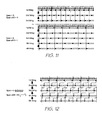
- Figure 11 shows a partial row of nozzles being fired with a span of three, and the same row segment with a span of five.
- the shift value is one. However, as discussed above, this is not an appropriate shift value in practice as the adjacent nozzles will fire consecutively. The turbulent wake from the drop fired from the first nozzle can interfere with the drop fired from the adjacent model immediately afterwards. It can also be a problem for the ink supply flow to the adjacent nozzles.
- span only controls the maximum number of nozzles that are able to fire at any one time.
- Each individual nozzle still needs a 1 in its shift register to actually fire.
- Figure 11 has a shift value of one. That is, one nozzle fires, then the next nozzle left fires, then the next, etc. As discussed above, this is impractical.
- Figure 12 shows a segment of the nozzle row with a span of 5 with a span shift of 3.
- the shift can not be a factor of the span, i.e. the span can not be divided by the shift (without remainder).
- the closest mutual prime to the square root of the span should be chosen for span shift. For example, for a span of 27, a span shift of 5 would be appropriate.
- Figures 13A and 13B show the relationship between region firing delay and current drain.
- Figure 13A shows the two extremes of power usage when printing a solid line of a color (this is the worst case for power supply because 80 dots will fire across the region).
- Figure 13A shows no firing delay between regions.
- Each region has 4 spans of 20 nozzles each.
- Each of the regions fire for the entire row time (row time is the time available for a complete row of nozzles to fire). Therefore, at any time during the row time, four nozzles from all of the eight regions are firing (drawing current).
- the profile of the supply current is a long flat step function 78 and identical for each region.
- the profile for the entire row is the accumulated step function 80 of the individual profiles 78.
- Theoretically the leading edge 90 of step function 80 is vertical but in fact it is very steep until it reaches the maximum current level 82. The high rate of change in the current can cause the undesirable voltage sags.
- Figure 13B shows the current supply profiles when the regions are fired in stages.
- the time in which the nozzles in each span can fire must be reduced.
- each span has half the row time in which to fire its nozzles.
- the number of nozzles in the span can be reduced.
- the cumulative current drawn for eight nozzles is greater than that for the four nozzles firing per span shown in Figure 13A . So the current drawn for each region in Figure 13B is twice that of the regions in Figure 13A , but the current is drawn for half the time.
- Region 1 is supply with current 84 at the beginning of the row time.
- the current supply 94 to region 2 starts after a set delay period and region 3 is similarly delayed relative to region 2, and so on until region 8 starts its firing sequence.
- the delays for each region need to be timed so that region 8 starts firing at or before half the row time has elapsed.
- the cumulative current supply profile 86 shows the series of 8 rapid steps in the current supply as it reaches its maximum value 88.
- the maximum current 88 is greater than the maximum current 82 in the non-delayed region firing, but the rate of increase in the supply current 92 is less. This induces less impedance in the circuit so that the voltage sag is lower. In each case, the total energy used is the same for a given row time but the distribution of energy consumption is adjusted.
- print data is sent to the printhead IC's 12 one row at a time followed by a fire command.
- each individual unit cell in the nozzle array had a shift register to store the print data (a '1' or '0') for each nozzle, for each line time (the line time is the time taken for the printhead to print one line of print).
- the print data for the entire array would be loaded into the shift registers before a fire command initiated the firing sequence.
- a smaller number of shift registers can be positioned adjacent the array instead of within each unit cell. Removing the shift registers from the unit cell 20 allows the drive FET 40 (see Figure 2 ) to be larger. This improves the printhead efficiency for the reasons set out below.
- Thermal printhead IC's are more efficient if the vapor bubble generated by heater element is nucleated quickly. Less heat dissipates into the ink prior to bubble nucleation. Faster nucleation of the bubble reduces the time that heat can diffuse into wafer regions surrounding the heater. To get the bubble to nucleate more quickly, the electrical pulse needs to have a shorter duration while still providing the same energy to the heater (about 200 nJ). This requires the drive FET for each nozzle to increase the power of the drive pulse. However, increasing the power of the drive FET increases its size. This enlarges the wafer area occupied by the nozzle and its associated circuitry and therefore reduces the nozzle density of the printhead. Reducing the nozzle density is detrimental to print quality and compact printhead design. By removing the shift register from the unit cell, the drive FET can be more powerful without compromising nozzle density.
- the Udon design writes data to the nozzle array one row at a time.
- a printhead IC that loaded and fired several rows at a time would also be achieving the similar benefits.
- the electrical connection between the shift register and the corresponding nozzle should be kept relatively short so as not to cause high resistive losses.
- Loading and firing the print data one row at a time requires the PEC to send the data in the row order that it is printed. Previously the data for the entire nozzle array was loaded before firing so the PEC was indifferent to the row firing order chosen by the printhead IC. With Udon, the PEC will need to transmit row data in a predetermined order.
- Printhead nozzles are normally fired according to the span/shift fire sequence and the delayed region start discussed above.
- the supply channels 50 in the back of the printhead IC 12 (see Figure 5C ) supply ink to two adjacent rows of nozzle on the front of the IC, that is rows 0 and 1 eject the same color, rows 2 and 3 eject another color, and so on.
- the Udon printhead IC has ten row of nozzles, these can be designated colors CMYK,IR (infra-red ink for encoding the media with data invisible to the eye) or CMYKK.
- every second row is fired in two passes, that is row 0, row 2, row 4, row 6, row 8, then row 1, row 3, row 5, and so on until all ten row are fired.
- Row firings should be timed such that each row takes just under 10% of the total line time to fire.
- a fire command simply fires the data that is currently loaded.
- Udon printhead IC receives a 'data next' command that loads the next row of data in the predetermined order.
- MoPEC mode each row of data must be specifically addressed to its row.
- Figure 14 shows the data flows and fire command sequences for a line of data.
- a fire command is received in the data stream
- the data in the row of shift registers transfers to a dot-latch in each of the unit cells, and a fire cycle is started to eject ink from every nozzle that has a 1 in its dot-latch. Meanwhile the data for the next row in the firing order is loaded.
- Drop compensation is the compensation applied by Udon drive logic 46 (see Figure 2 ) to the sloping region 28 and drop triangle 30 of nozzles at the left of the nozzle array22 on each IC 12 (see Figure 5C ).
- the print data to the nozzles that are displaced from the rest of the array 22 needs to be delayed by a certain number of line times.
- Figure 15 shows the nozzles in one row 26 of the IC 12.
- the nozzles in the drop triangle 30 are all displaced 10 dot pitches from the non-displaced nozzles in the row.
- the nozzles in the droop section 28 that connects the drop triangle 30 and the non-displaced nozzles have a displacement that indexes by one dot pitch every two nozzles.
- the drive logic indexes the delay in firing the dot data correspondingly.
- nozzles may become blocked with more viscous or dried ink. Water can evaporate from the ink in the nozzles thereby increasing the viscosity of the ink to the point where the bubble is unable to eject the drop. The nozzle becomes clogged and inoperable.
- printers have a printhead maintenance regime that can recover clogged nozzles and clean the exterior face of the printhead. These create a vacuum to suck the ink through the nozzle so that the less viscous ink refills the nozzle. A relatively large volume of ink is wasted by this process requiring the cartridges to be replaced more frequently.
- Udon printhead IC's have a maintenance mode that can operate before or during a print job.
- the drive logic generates a de-clog pulse for the actuators in each nozzle unless the dead nozzle map (described below) indicates that the actuator has failed.
- the nozzles should fire the de-clog pulse into the gap between pages without interruption to the paper.
- the de-clog pulse is longer than the normal drive pulses.
- the bubble formed from a longer duration pulse is larger and imparts a greater impulse to the ink than a firing impulse. This gives the pulse the additional force that may be needed to eject high viscosity ink.
- the de-clog pulse can be preceded by a series of sub-ejection pulses to warm the ink and lower viscosity.
- Figure 16 shows a typical de-clog pulse train with a series of short (relative to a firing pulse) sub-ejection pulses 94 followed by a single de-clog pulse 96.
- the individual sub-ejection pulses 94 have insufficient energy to nucleate a bubble and therefore eject ink. However, a rapid series of them raises the ink temperature to assist the subsequent de-clog pulse 96.
- the Udon printhead IC 12 supports an open actuator test.
- the open actuator test (OAT) is used to discover whether any actuators in the nozzles array have burnt out and fractured (usually referred to as becoming 'open' or 'open circuit').
- Fabrication of the MEMS nozzle structures on wafer substrates will invariably result in some defective nozzles.
- These 'dead nozzles' can be located using a wafer probe immediately after fabrication. Knowing the location of the dead nozzles, the print engine controller (PEC) can be programmed with a dead nozzle map. This is used to compensate for the dead nozzles with techniques such as nozzle redundancy (the printhead IC is has more nozzles than necessary and uses the 'spare' nozzles to print the dots normally assigned to the dead nozzles).
- nozzles also fail during the operational-life of the printhead. It is not possible to locate these nozzles using a wafer probe once they have been mounted to the printhead assembly and installed in the printer. Over time, the number of dead nozzles increases and as the PEC is not aware of them, there is no attempt to compensate for them. This eventually causes visible artifacts that are detrimental to the print quality.
- the vast majority of failures are the result of the resistive heater burning out or going open circuit.
- Nozzles may fail to eject ink because of clogging but this is not a 'dead nozzle,' and may be recovered through the printer maintenance regime.
- the print engine controller can periodically update its dead nozzle map. With an accurate dead nozzles map, the PEC can use compensation techniques (e.g. nozzle redundancy) to extend the operational life of the printhead.
- the Udon IC open actuator test compares the resistance of the actuator to a predetermined threshold. A high (or infinite) resistance indicates that the actuator has failed and this information is fed back to the PEC to update its dead nozzle compensation tables. It is important to note that the OAT can discover open circuit nozzles, but not clogged nozzles.
- Thermal actuators and thermal bend actuator both use heater elements and the OAT can be equally applied to either.
- the drive FET can be N-type or P-type.
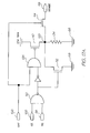
- Figure 17A and 17B show the circuits for the OAT as applied to a single unit cell with a single heater element driven by a p-FET and an n-FET respectively.
- the drive p-FET 40 is enabled during printing whenever the 'row enable' (RE) 98 and 'column enable' (CE) 100 are both asserted (receive '1's at their contacts). Enabling the drive FET 40 opens the heater element 34 to Vpos 104 to activate the unit cell. When the row enable 98 or the column enable 100 are not asserted, the bleed n-FET is enabled. The bleed n-FET 112 ensures that the voltage at the sense node 120 is pulled low when the unit cell is not activated to eliminate any electrolysis path.
- RE 'row enable'
- CE 'column enable'
- the AND gate 108 pulls the gate of the drive p-FET 40 high to disable it. Asserting the OAT 106 also pulls the gate of the sense n-FET 114 high to connect the sense output 116 to the sense node 120. With the bleed n-FET 112 disabled the voltage at the sense node 120 will still be pulled low through the heater element 34 to ground 68. Accordingly, the sense output 116 is low to indicate that the actuator is still operational. However, if the heater element 34 is open (failed), the voltage at the sense node 120 remains high and this pulls the sense output 116 high to indicate a dead nozzle. This is fed back to the PEC which updates the dead nozzle map and initiates measures to compensate (if possible).
- the unit cell circuitry shown in Figure 17B uses a drive n-FET 40.
- asserting the row enable 98 and the column enable 100 pulls the gate of the drive n-FET 40 high to enable it and allow Vpos 104 to drain to ground through the heater 34.
- the bleed p-FET 118 is disabled whenever the row enable 98 and column enable 100 are asserted.
- the OAT 106 is asserted, together with the row enable 98 and column enable 100. This disables the drive n-FET 40 by pulling the gate low using NAND logic 110. It also opens the sense n-FET 114 to connect the sense output 116 to the sense node 120. With the heater 34 insulated from ground 68 when the drive FET 40 is disabled, the sense node 120 is pulled high and a high sense output 116 indicates a working actuator. If the heater 34 is broken, the sense node 120 is left at low voltage following the last time the drive FET 40 was enabled. Accordingly when the OAT is enabled, the sense output 116 is low and the PEC records the dead nozzle to the dead nozzle map.
- the open actuator test should be performed shortly after the printhead IC has been printing. After a period of inactivity, the bleed p-FET 118 or n-FET 112 drops the sense node to low voltage. The gap in printing between pages is a convenient opportunity to perform an open actuator test.
Landscapes
- Engineering & Computer Science (AREA)
- Quality & Reliability (AREA)
- Particle Formation And Scattering Control In Inkjet Printers (AREA)
- Ink Jet (AREA)
Claims (13)
- Imprimante à jet d'encre comprenant :un réseau (22) de buses (32) agencées en rangées (26), chaque rangée (26) consistant en une pluralité de groupes de buses, les buses (32) dans chaque groupe étant entrecoupées de buses (32) d'autres groupes ; et,des circuits de commande associés (42, 46) pour actionner les buses (32) dans la rangée (26) selon une séquence de déclenchement, la séquence de déclenchement activant les buses dans chaque groupe pour éjecter simultanément du fluide d'impression, et activant chacun des groupes pour éjecter successivement du fluide d'impression ;dans laquelle :chaque rangée est divisée en plages, chaque plage ayant seulement une buse de chaque groupe de telle sorte que le nombre de plages sur toute la rangée (26) est égal au nombre de groupes de buses ;les buses (32) dans chaque groupe sont espacées les unes des autres par au moins un nombre minimal prédéterminé de buses (32) ; etchacune des buses dans un groupe est espacée des buses (32) dans le groupe activé ensuite par au moinsle nombre minimal prédéterminé de buses (32) caractérisée par le fait que :le nombre minimal prédéterminé de buses (32) entre des buses activées de façon séquentielle est un décalage uniforme le long de chaque plage dans une direction uniforme, le décalage étant un nombre de buses qui est un entier supérieur à un et qui n'est pas un facteur du nombre de buses (32) dans la plage.
- Imprimante à jet d'encre selon la revendication 1, dans laquelle les buses activées successivement (32) dans chaque plage avancent à partir d'une première extrémité vers une seconde extrémité de la plage jusqu'à ce qu'il n'y ait pas suffisamment de buses (32) à la seconde extrémité pour remplir le décalage, auquel cas le décalage est terminé par activation d'une buse non activée à la première extrémité de la plage jusqu'à ce que toutes les buses (32) dans la plage soient activées une fois pendant la séquence de déclenchement.
- Imprimante à jet d'encre selon la revendication 1, dans laquelle le décalage est le nombre de buses (32) qui est l'entier le plus proche de la racine carrée de la plage et qui n'est pas un facteur de la plage.
- Imprimante à jet d'encre selon l'une quelconque des revendications précédentes, comprenant en outre une pluralité de capteurs de température (74) positionnés le long du réseau (22) de buses (32) de telle sorte que les circuits de commande (42, 46) ajustent les impulsions de commande en réponse aux sorties des capteurs de température (74).
- Imprimante à jet d'encre selon la revendication 4, dans laquelle chacun de la pluralité de capteurs de température (74) est activé de façon séquentielle pendant une période de temps lors du travail d'impression.
- Imprimante à jet d'encre selon l'une des revendications 4 ou 5, dans laquelle la pluralité de capteurs de température (74) est divisée en deux ou plusieurs groupes, chaque groupe étant activé pendant une période de détection selon une séquence de répétition prédéterminée pendant la durée d'un travail d'impression.
- Imprimante à jet d'encre selon la revendication 6, dans laquelle chacun de la pluralité de capteurs de température (74) est configuré pour détecter la température d'une région correspondante du réseau (22) de telle sorte que l'impulsion de commande pour les buses (32) dans une région peut différer de l'impulsion de commande pour les buses (32) dans une autre région.
- Imprimante à jet d'encre selon la revendication 4, dans laquelle un capteur de température sur deux dans la pluralité de capteurs de température (74) est désactivé de telle sorte que les circuits de commande (42, 46) ajustent le profil d'impulsion de commande pour la région correspondant à chaque capteur de température activé (74) et applique le même ajustement à la région adjacente dans laquelle le capteur de température (74) est désactivé.
- Imprimante à jet d'encre selon la revendication 4, dans laquelle les circuits de commande (42, 46) sont programmés avec une série de seuils de température définissant un ensemble de zones de température, chacune des zones ayant un profil d'impulsion différent pour les impulsions de commande envoyées aux buses (32) dans la région fonctionnant actuellement dans cette zone de température.
- Imprimante à jet d'encre selon la revendication 9, dans laquelle le profil d'impulsion pour chaque zone de température diffère en durée.
- Imprimante à jet d'encre selon la revendication 10, dans laquelle les circuits de commande (42, 46) règlent la durée d'impulsion à zéro si le capteur de température (74) indique que la région fonctionne à une température au-dessus du seuil le plus haut parmi les seuils de température.
- Imprimante à jet d'encre selon la revendication 11, dans laquelle les circuits de commande (42, 46) règlent la durée du profil d'impulsion à une valeur de sous-éjection pour l'une quelconque des buses (32) dans la rangée (26) qui ne doivent pas éjecter une goutte pendant cette séquence de déclenchement.
- Imprimante à jet d'encre selon l'une quelconque des revendications précédentes, dans laquelle les circuits de commande (42, 46) sont configurés pour fonctionner dans deux modes : un mode d'impression dans lequel les impulsions de commande générées sont des impulsions d'impression, et un mode d'entretien dans lequel les impulsions de commande générées sont des impulsions de désobstruction, de telle sorte que l'impulsion de désobstruction a une plus longue durée que l'impulsion d'impression.
Priority Applications (1)
| Application Number | Priority Date | Filing Date | Title |
|---|---|---|---|
| EP13151348.3A EP2583833B1 (fr) | 2006-10-09 | 2006-10-09 | Imprimante à jet d'encre comprenant une séquence de démarrage de gicleur |
Applications Claiming Priority (3)
| Application Number | Priority Date | Filing Date | Title |
|---|---|---|---|
| EP13151348.3A EP2583833B1 (fr) | 2006-10-09 | 2006-10-09 | Imprimante à jet d'encre comprenant une séquence de démarrage de gicleur |
| EP06790345A EP2073983A4 (fr) | 2006-10-09 | 2006-10-09 | Circuit intégré de tête d'impression avec test d'actionneur ouvert |
| PCT/AU2006/001475 WO2008043120A1 (fr) | 2006-10-09 | 2006-10-09 | Circuit intégré de tête d'impression avec test d'actionneur ouvert |
Related Parent Applications (2)
| Application Number | Title | Priority Date | Filing Date |
|---|---|---|---|
| EP06790345.0 Division | 2006-10-09 | ||
| EP06790345A Division EP2073983A4 (fr) | 2006-10-09 | 2006-10-09 | Circuit intégré de tête d'impression avec test d'actionneur ouvert |
Publications (2)
| Publication Number | Publication Date |
|---|---|
| EP2583833A1 EP2583833A1 (fr) | 2013-04-24 |
| EP2583833B1 true EP2583833B1 (fr) | 2014-02-26 |
Family
ID=39282324
Family Applications (2)
| Application Number | Title | Priority Date | Filing Date |
|---|---|---|---|
| EP13151348.3A Not-in-force EP2583833B1 (fr) | 2006-10-09 | 2006-10-09 | Imprimante à jet d'encre comprenant une séquence de démarrage de gicleur |
| EP06790345A Withdrawn EP2073983A4 (fr) | 2006-10-09 | 2006-10-09 | Circuit intégré de tête d'impression avec test d'actionneur ouvert |
Family Applications After (1)
| Application Number | Title | Priority Date | Filing Date |
|---|---|---|---|
| EP06790345A Withdrawn EP2073983A4 (fr) | 2006-10-09 | 2006-10-09 | Circuit intégré de tête d'impression avec test d'actionneur ouvert |
Country Status (6)
| Country | Link |
|---|---|
| EP (2) | EP2583833B1 (fr) |
| JP (1) | JP2010505642A (fr) |
| KR (1) | KR101098595B1 (fr) |
| CN (1) | CN101522428B (fr) |
| TW (1) | TWI380908B (fr) |
| WO (1) | WO2008043120A1 (fr) |
Families Citing this family (15)
| Publication number | Priority date | Publication date | Assignee | Title |
|---|---|---|---|---|
| JP5169599B2 (ja) * | 2008-08-04 | 2013-03-27 | セイコーエプソン株式会社 | 液体吐出装置 |
| CN107000437B (zh) | 2014-10-28 | 2019-01-11 | 惠普发展公司,有限责任合伙企业 | 宽阵列打印头模块 |
| US9597893B2 (en) | 2015-01-06 | 2017-03-21 | Canon Kabushiki Kaisha | Element substrate and liquid discharge head |
| JP6470570B2 (ja) * | 2015-01-06 | 2019-02-13 | キヤノン株式会社 | 素子基板、液体吐出ヘッド及び記録装置 |
| WO2018186850A1 (fr) * | 2017-04-05 | 2018-10-11 | Hewlett-Packard Development Company, L.P. | Désactivation d'actionneur de matrice |
| WO2018186852A1 (fr) * | 2017-04-05 | 2018-10-11 | Hewlett-Packard Development Company, L.P. | Détection de défaillance d'actionneur sur matrice |
| TWI666126B (zh) * | 2018-09-28 | 2019-07-21 | 謙華科技股份有限公司 | 打印頭裝置及列印方法 |
| CN111152561B (zh) * | 2018-11-07 | 2021-02-09 | 杭州旗捷科技有限公司 | 墨盒验证方法、系统、可读存储介质和设备 |
| CN113165389A (zh) * | 2018-12-03 | 2021-07-23 | 惠普发展公司,有限责任合伙企业 | 逻辑电路系统封装 |
| CN115723430A (zh) | 2019-02-06 | 2023-03-03 | 惠普发展公司,有限责任合伙企业 | 打印部件和操作打印部件的方法 |
| MX2021009124A (es) | 2019-02-06 | 2021-09-08 | Hewlett Packard Development Co | Componente de impresion que tiene estructuras de accionamiento fluidico con diferentes arquitecturas fluidicas. |
| EP3717254B1 (fr) | 2019-02-06 | 2023-12-20 | Hewlett-Packard Development Company, L.P. | Circuit intégré à circuits d'attaque d'adresse pour puce fluidique |
| PL4206896T3 (pl) | 2019-02-06 | 2024-10-28 | Hewlett-Packard Development Company L.P. | Identyfikacja bitów losowych w pakietach danych sterujących |
| BR112021014154A2 (pt) | 2019-02-06 | 2021-09-21 | Hewlett-Packard Development Company, L.P. | Monitor de reset |
| MX2021009109A (es) * | 2019-02-06 | 2021-09-14 | Hewlett Packard Development Co | Matriz para un cabezal de impresion. |
Family Cites Families (21)
| Publication number | Priority date | Publication date | Assignee | Title |
|---|---|---|---|---|
| US4595935A (en) * | 1984-08-14 | 1986-06-17 | Ncr Canada Ltd. | System for detecting defective thermal printhead elements |
| US4716519A (en) * | 1986-01-22 | 1987-12-29 | Nordson Corporation | Method of checking channel connections and detecting heater circuit and temperature sensor malfunctions in multi-channel closed loop hot melt heating systems |
| JPH04211961A (ja) * | 1990-02-26 | 1992-08-03 | Canon Inc | インクジェット記録装置および情報処理装置 |
| AU657720B2 (en) * | 1991-01-30 | 1995-03-23 | Canon Kabushiki Kaisha | A bubblejet image reproducing apparatus |
| JP3005136B2 (ja) * | 1992-04-27 | 2000-01-31 | キヤノン株式会社 | プリント装置およびプリント方法 |
| US5363134A (en) * | 1992-05-20 | 1994-11-08 | Hewlett-Packard Corporation | Integrated circuit printhead for an ink jet printer including an integrated identification circuit |
| JPH0768907A (ja) * | 1993-09-01 | 1995-03-14 | Fujitsu Ltd | インクジェットヘッド |
| JP3308717B2 (ja) * | 1994-07-21 | 2002-07-29 | キヤノン株式会社 | 記録装置及び記録方法 |
| US5736997A (en) * | 1996-04-29 | 1998-04-07 | Lexmark International, Inc. | Thermal ink jet printhead driver overcurrent protection scheme |
| KR100197460B1 (ko) * | 1996-09-17 | 1999-06-15 | 윤종용 | 잉크젯 프린터의 노즐구동 검사장치 및 방법 |
| CA2298530A1 (fr) * | 1997-08-01 | 1999-02-25 | David Neese | Imprimante a jet d'encre, et procede et systeme permettant de compenser le non-fonctionnement de certains elements d'impression |
| US6733116B1 (en) * | 1998-10-16 | 2004-05-11 | Silverbrook Research Pty Ltd | Ink jet printer with print roll and printhead assemblies |
| US6375299B1 (en) * | 1998-11-02 | 2002-04-23 | Encad, Inc. | Faulty ink ejector detection in an ink jet printer |
| AUPP702498A0 (en) * | 1998-11-09 | 1998-12-03 | Silverbrook Research Pty Ltd | Image creation method and apparatus (ART77) |
| US6631986B2 (en) * | 1998-12-16 | 2003-10-14 | Silverbrook Research Pty Ltd | Printer transport roller with internal drive motor |
| CN1689814B (zh) * | 2000-05-24 | 2011-07-27 | 西尔弗布鲁克研究有限公司 | 打印引擎控制器、打印机和处理图像数据的方法 |
| JP4221953B2 (ja) * | 2002-05-29 | 2009-02-12 | セイコーエプソン株式会社 | インクジェット式プリンタのヘッドドライバic温度検出回路の故障検出装置及び方法 |
| US6760053B2 (en) * | 2002-04-29 | 2004-07-06 | Rimage Corporation | Thermal printer element tester |
| KR100528342B1 (ko) * | 2003-07-02 | 2005-11-15 | 삼성전자주식회사 | 잉크젯 프린트헤드의 구동방법 |
| US6799837B1 (en) * | 2003-07-07 | 2004-10-05 | Benq Corporation | Ink jet printing apparatus with ink level detection |
| US7314261B2 (en) * | 2004-05-27 | 2008-01-01 | Silverbrook Research Pty Ltd | Printhead module for expelling ink from nozzles in groups, alternately, starting at outside nozzles of each group |
-
2006
- 2006-10-09 JP JP2009530733A patent/JP2010505642A/ja active Pending
- 2006-10-09 CN CN2006800560609A patent/CN101522428B/zh not_active Expired - Fee Related
- 2006-10-09 WO PCT/AU2006/001475 patent/WO2008043120A1/fr not_active Ceased
- 2006-10-09 EP EP13151348.3A patent/EP2583833B1/fr not_active Not-in-force
- 2006-10-09 KR KR1020097008430A patent/KR101098595B1/ko not_active Expired - Fee Related
- 2006-10-09 EP EP06790345A patent/EP2073983A4/fr not_active Withdrawn
-
2007
- 2007-02-01 TW TW096103749A patent/TWI380908B/zh not_active IP Right Cessation
Also Published As
| Publication number | Publication date |
|---|---|
| TW200817189A (en) | 2008-04-16 |
| JP2010505642A (ja) | 2010-02-25 |
| EP2583833A1 (fr) | 2013-04-24 |
| WO2008043120A1 (fr) | 2008-04-17 |
| KR101098595B1 (ko) | 2011-12-23 |
| CN101522428B (zh) | 2011-10-05 |
| EP2073983A4 (fr) | 2012-08-01 |
| EP2073983A1 (fr) | 2009-07-01 |
| TWI380908B (zh) | 2013-01-01 |
| CN101522428A (zh) | 2009-09-02 |
| KR20090094430A (ko) | 2009-09-07 |
Similar Documents
| Publication | Publication Date | Title |
|---|---|---|
| US7591523B2 (en) | Printhead IC with de-activatable temperature sensor and maintenance mode | |
| US7384128B2 (en) | Printhead IC with nozzle array for linking with adjacent printhead IC's | |
| US7874633B2 (en) | Printhead IC with non-ejection maintenance | |
| US7891748B2 (en) | Print engine controller having controller circuitry with an open actuator test circuit | |
| US8075099B2 (en) | Printer with controller for generating combined print data and clock signal | |
| EP2583833B1 (fr) | Imprimante à jet d'encre comprenant une séquence de démarrage de gicleur | |
| US7695091B2 (en) | Test circuitry for a printhead nozzle arrangement | |
| US7819494B2 (en) | Printhead IC with multi-stage print data loading and firing | |
| US8016389B2 (en) | Printhead IC with staggered nozzle firing pulses | |
| US7681970B2 (en) | Self initialising printhead IC | |
| US7946674B2 (en) | Printhead IC with open actuator test | |
| US7938500B2 (en) | Printhead IC with multiple temperature sensors | |
| US7780256B2 (en) | Printhead IC with spaced nozzle firing sequence | |
| US20080084434A1 (en) | Printhead IC with pulse profile adjustment |
Legal Events
| Date | Code | Title | Description |
|---|---|---|---|
| PUAI | Public reference made under article 153(3) epc to a published international application that has entered the european phase |
Free format text: ORIGINAL CODE: 0009012 |
|
| AC | Divisional application: reference to earlier application |
Ref document number: 2073983 Country of ref document: EP Kind code of ref document: P |
|
| AK | Designated contracting states |
Kind code of ref document: A1 Designated state(s): AT BE BG CH CY CZ DE DK EE ES FI FR GB GR HU IE IS IT LI LT LU LV MC NL PL PT RO SE SI SK TR |
|
| 17P | Request for examination filed |
Effective date: 20130925 |
|
| RBV | Designated contracting states (corrected) |
Designated state(s): AT BE BG CH CY CZ DE DK EE ES FI FR GB GR HU IE IS IT LI LT LU LV MC NL PL PT RO SE SI SK TR |
|
| GRAP | Despatch of communication of intention to grant a patent |
Free format text: ORIGINAL CODE: EPIDOSNIGR1 |
|
| INTG | Intention to grant announced |
Effective date: 20131203 |
|
| GRAS | Grant fee paid |
Free format text: ORIGINAL CODE: EPIDOSNIGR3 |
|
| GRAA | (expected) grant |
Free format text: ORIGINAL CODE: 0009210 |
|
| RAP1 | Party data changed (applicant data changed or rights of an application transferred) |
Owner name: ZAMTEC LIMITED |
|
| AC | Divisional application: reference to earlier application |
Ref document number: 2073983 Country of ref document: EP Kind code of ref document: P |
|
| AK | Designated contracting states |
Kind code of ref document: B1 Designated state(s): AT BE BG CH CY CZ DE DK EE ES FI FR GB GR HU IE IS IT LI LT LU LV MC NL PL PT RO SE SI SK TR |
|
| REG | Reference to a national code |
Ref country code: GB Ref legal event code: FG4D |
|
| REG | Reference to a national code |
Ref country code: CH Ref legal event code: EP |
|
| REG | Reference to a national code |
Ref country code: AT Ref legal event code: REF Ref document number: 653330 Country of ref document: AT Kind code of ref document: T Effective date: 20140315 |
|
| REG | Reference to a national code |
Ref country code: IE Ref legal event code: FG4D |
|
| REG | Reference to a national code |
Ref country code: DE Ref legal event code: R096 Ref document number: 602006040455 Country of ref document: DE Effective date: 20140410 |
|
| REG | Reference to a national code |
Ref country code: NL Ref legal event code: VDEP Effective date: 20140226 |
|
| REG | Reference to a national code |
Ref country code: AT Ref legal event code: MK05 Ref document number: 653330 Country of ref document: AT Kind code of ref document: T Effective date: 20140226 |
|
| REG | Reference to a national code |
Ref country code: LT Ref legal event code: MG4D |
|
| PG25 | Lapsed in a contracting state [announced via postgrant information from national office to epo] |
Ref country code: IS Free format text: LAPSE BECAUSE OF FAILURE TO SUBMIT A TRANSLATION OF THE DESCRIPTION OR TO PAY THE FEE WITHIN THE PRESCRIBED TIME-LIMIT Effective date: 20140626 Ref country code: LT Free format text: LAPSE BECAUSE OF FAILURE TO SUBMIT A TRANSLATION OF THE DESCRIPTION OR TO PAY THE FEE WITHIN THE PRESCRIBED TIME-LIMIT Effective date: 20140226 |
|
| RAP2 | Party data changed (patent owner data changed or rights of a patent transferred) |
Owner name: MEMJET TECHNOLOLGY LIMITED |
|
| PG25 | Lapsed in a contracting state [announced via postgrant information from national office to epo] |
Ref country code: AT Free format text: LAPSE BECAUSE OF FAILURE TO SUBMIT A TRANSLATION OF THE DESCRIPTION OR TO PAY THE FEE WITHIN THE PRESCRIBED TIME-LIMIT Effective date: 20140226 Ref country code: FI Free format text: LAPSE BECAUSE OF FAILURE TO SUBMIT A TRANSLATION OF THE DESCRIPTION OR TO PAY THE FEE WITHIN THE PRESCRIBED TIME-LIMIT Effective date: 20140226 Ref country code: NL Free format text: LAPSE BECAUSE OF FAILURE TO SUBMIT A TRANSLATION OF THE DESCRIPTION OR TO PAY THE FEE WITHIN THE PRESCRIBED TIME-LIMIT Effective date: 20140226 Ref country code: CY Free format text: LAPSE BECAUSE OF FAILURE TO SUBMIT A TRANSLATION OF THE DESCRIPTION OR TO PAY THE FEE WITHIN THE PRESCRIBED TIME-LIMIT Effective date: 20140226 Ref country code: PT Free format text: LAPSE BECAUSE OF FAILURE TO SUBMIT A TRANSLATION OF THE DESCRIPTION OR TO PAY THE FEE WITHIN THE PRESCRIBED TIME-LIMIT Effective date: 20140626 Ref country code: SE Free format text: LAPSE BECAUSE OF FAILURE TO SUBMIT A TRANSLATION OF THE DESCRIPTION OR TO PAY THE FEE WITHIN THE PRESCRIBED TIME-LIMIT Effective date: 20140226 |
|
| RAP2 | Party data changed (patent owner data changed or rights of a patent transferred) |
Owner name: MEMJET TECHNOLOGY LIMITED |
|
| PG25 | Lapsed in a contracting state [announced via postgrant information from national office to epo] |
Ref country code: LV Free format text: LAPSE BECAUSE OF FAILURE TO SUBMIT A TRANSLATION OF THE DESCRIPTION OR TO PAY THE FEE WITHIN THE PRESCRIBED TIME-LIMIT Effective date: 20140226 Ref country code: BE Free format text: LAPSE BECAUSE OF FAILURE TO SUBMIT A TRANSLATION OF THE DESCRIPTION OR TO PAY THE FEE WITHIN THE PRESCRIBED TIME-LIMIT Effective date: 20140226 |
|
| PG25 | Lapsed in a contracting state [announced via postgrant information from national office to epo] |
Ref country code: CZ Free format text: LAPSE BECAUSE OF FAILURE TO SUBMIT A TRANSLATION OF THE DESCRIPTION OR TO PAY THE FEE WITHIN THE PRESCRIBED TIME-LIMIT Effective date: 20140226 Ref country code: RO Free format text: LAPSE BECAUSE OF FAILURE TO SUBMIT A TRANSLATION OF THE DESCRIPTION OR TO PAY THE FEE WITHIN THE PRESCRIBED TIME-LIMIT Effective date: 20140226 Ref country code: DK Free format text: LAPSE BECAUSE OF FAILURE TO SUBMIT A TRANSLATION OF THE DESCRIPTION OR TO PAY THE FEE WITHIN THE PRESCRIBED TIME-LIMIT Effective date: 20140226 Ref country code: EE Free format text: LAPSE BECAUSE OF FAILURE TO SUBMIT A TRANSLATION OF THE DESCRIPTION OR TO PAY THE FEE WITHIN THE PRESCRIBED TIME-LIMIT Effective date: 20140226 |
|
| REG | Reference to a national code |
Ref country code: DE Ref legal event code: R097 Ref document number: 602006040455 Country of ref document: DE Ref country code: DE Ref legal event code: R081 Ref document number: 602006040455 Country of ref document: DE Owner name: MEMJET TECHNOLOGY LIMITED, IE Free format text: FORMER OWNER: ZAMTEC LTD., DUBLIN, IE Effective date: 20141016 |
|
| PG25 | Lapsed in a contracting state [announced via postgrant information from national office to epo] |
Ref country code: PL Free format text: LAPSE BECAUSE OF FAILURE TO SUBMIT A TRANSLATION OF THE DESCRIPTION OR TO PAY THE FEE WITHIN THE PRESCRIBED TIME-LIMIT Effective date: 20140226 Ref country code: ES Free format text: LAPSE BECAUSE OF FAILURE TO SUBMIT A TRANSLATION OF THE DESCRIPTION OR TO PAY THE FEE WITHIN THE PRESCRIBED TIME-LIMIT Effective date: 20140226 Ref country code: SK Free format text: LAPSE BECAUSE OF FAILURE TO SUBMIT A TRANSLATION OF THE DESCRIPTION OR TO PAY THE FEE WITHIN THE PRESCRIBED TIME-LIMIT Effective date: 20140226 |
|
| PLBE | No opposition filed within time limit |
Free format text: ORIGINAL CODE: 0009261 |
|
| STAA | Information on the status of an ep patent application or granted ep patent |
Free format text: STATUS: NO OPPOSITION FILED WITHIN TIME LIMIT |
|
| 26N | No opposition filed |
Effective date: 20141127 |
|
| REG | Reference to a national code |
Ref country code: DE Ref legal event code: R097 Ref document number: 602006040455 Country of ref document: DE Effective date: 20141127 |
|
| PG25 | Lapsed in a contracting state [announced via postgrant information from national office to epo] |
Ref country code: IT Free format text: LAPSE BECAUSE OF FAILURE TO SUBMIT A TRANSLATION OF THE DESCRIPTION OR TO PAY THE FEE WITHIN THE PRESCRIBED TIME-LIMIT Effective date: 20140226 |
|
| PG25 | Lapsed in a contracting state [announced via postgrant information from national office to epo] |
Ref country code: LU Free format text: LAPSE BECAUSE OF FAILURE TO SUBMIT A TRANSLATION OF THE DESCRIPTION OR TO PAY THE FEE WITHIN THE PRESCRIBED TIME-LIMIT Effective date: 20141009 Ref country code: MC Free format text: LAPSE BECAUSE OF FAILURE TO SUBMIT A TRANSLATION OF THE DESCRIPTION OR TO PAY THE FEE WITHIN THE PRESCRIBED TIME-LIMIT Effective date: 20140226 Ref country code: SI Free format text: LAPSE BECAUSE OF FAILURE TO SUBMIT A TRANSLATION OF THE DESCRIPTION OR TO PAY THE FEE WITHIN THE PRESCRIBED TIME-LIMIT Effective date: 20140226 |
|
| REG | Reference to a national code |
Ref country code: CH Ref legal event code: PL |
|
| PG25 | Lapsed in a contracting state [announced via postgrant information from national office to epo] |
Ref country code: CH Free format text: LAPSE BECAUSE OF NON-PAYMENT OF DUE FEES Effective date: 20141031 Ref country code: LI Free format text: LAPSE BECAUSE OF NON-PAYMENT OF DUE FEES Effective date: 20141031 |
|
| REG | Reference to a national code |
Ref country code: FR Ref legal event code: PLFP Year of fee payment: 10 |
|
| PG25 | Lapsed in a contracting state [announced via postgrant information from national office to epo] |
Ref country code: BG Free format text: LAPSE BECAUSE OF FAILURE TO SUBMIT A TRANSLATION OF THE DESCRIPTION OR TO PAY THE FEE WITHIN THE PRESCRIBED TIME-LIMIT Effective date: 20140226 |
|
| PG25 | Lapsed in a contracting state [announced via postgrant information from national office to epo] |
Ref country code: GR Free format text: LAPSE BECAUSE OF FAILURE TO SUBMIT A TRANSLATION OF THE DESCRIPTION OR TO PAY THE FEE WITHIN THE PRESCRIBED TIME-LIMIT Effective date: 20140527 |
|
| PG25 | Lapsed in a contracting state [announced via postgrant information from national office to epo] |
Ref country code: TR Free format text: LAPSE BECAUSE OF FAILURE TO SUBMIT A TRANSLATION OF THE DESCRIPTION OR TO PAY THE FEE WITHIN THE PRESCRIBED TIME-LIMIT Effective date: 20140226 Ref country code: HU Free format text: LAPSE BECAUSE OF FAILURE TO SUBMIT A TRANSLATION OF THE DESCRIPTION OR TO PAY THE FEE WITHIN THE PRESCRIBED TIME-LIMIT; INVALID AB INITIO Effective date: 20061009 |
|
| REG | Reference to a national code |
Ref country code: FR Ref legal event code: PLFP Year of fee payment: 11 |
|
| REG | Reference to a national code |
Ref country code: FR Ref legal event code: PLFP Year of fee payment: 12 |
|
| PGFP | Annual fee paid to national office [announced via postgrant information from national office to epo] |
Ref country code: FR Payment date: 20171025 Year of fee payment: 12 |
|
| PGFP | Annual fee paid to national office [announced via postgrant information from national office to epo] |
Ref country code: IE Payment date: 20171031 Year of fee payment: 12 |
|
| REG | Reference to a national code |
Ref country code: IE Ref legal event code: MM4A |
|
| PG25 | Lapsed in a contracting state [announced via postgrant information from national office to epo] |
Ref country code: FR Free format text: LAPSE BECAUSE OF NON-PAYMENT OF DUE FEES Effective date: 20181031 |
|
| PG25 | Lapsed in a contracting state [announced via postgrant information from national office to epo] |
Ref country code: IE Free format text: LAPSE BECAUSE OF NON-PAYMENT OF DUE FEES Effective date: 20181009 |
|
| PGFP | Annual fee paid to national office [announced via postgrant information from national office to epo] |
Ref country code: GB Payment date: 20211027 Year of fee payment: 16 Ref country code: DE Payment date: 20211027 Year of fee payment: 16 |
|
| REG | Reference to a national code |
Ref country code: DE Ref legal event code: R119 Ref document number: 602006040455 Country of ref document: DE |
|
| GBPC | Gb: european patent ceased through non-payment of renewal fee |
Effective date: 20221009 |
|
| PG25 | Lapsed in a contracting state [announced via postgrant information from national office to epo] |
Ref country code: DE Free format text: LAPSE BECAUSE OF NON-PAYMENT OF DUE FEES Effective date: 20230503 |
|
| PG25 | Lapsed in a contracting state [announced via postgrant information from national office to epo] |
Ref country code: GB Free format text: LAPSE BECAUSE OF NON-PAYMENT OF DUE FEES Effective date: 20221009 |