EP2584601B1 - Verfahren zur Herstellung einer Halbleitervorrichtung mit dualer Austrittsarbeit - Google Patents
Verfahren zur Herstellung einer Halbleitervorrichtung mit dualer Austrittsarbeit Download PDFInfo
- Publication number
- EP2584601B1 EP2584601B1 EP13152000.9A EP13152000A EP2584601B1 EP 2584601 B1 EP2584601 B1 EP 2584601B1 EP 13152000 A EP13152000 A EP 13152000A EP 2584601 B1 EP2584601 B1 EP 2584601B1
- Authority
- EP
- European Patent Office
- Prior art keywords
- gate
- layer
- work function
- metal
- metal layer
- Prior art date
- Legal status (The legal status is an assumption and is not a legal conclusion. Google has not performed a legal analysis and makes no representation as to the accuracy of the status listed.)
- Active
Links
Images





Classifications
-
- H—ELECTRICITY
- H10—SEMICONDUCTOR DEVICES; ELECTRIC SOLID-STATE DEVICES NOT OTHERWISE PROVIDED FOR
- H10D—INORGANIC ELECTRIC SEMICONDUCTOR DEVICES
- H10D84/00—Integrated devices formed in or on semiconductor substrates that comprise only semiconducting layers, e.g. on Si wafers or on GaAs-on-Si wafers
- H10D84/01—Manufacture or treatment
- H10D84/0123—Integrating together multiple components covered by H10D12/00 or H10D30/00, e.g. integrating multiple IGBTs
- H10D84/0126—Integrating together multiple components covered by H10D12/00 or H10D30/00, e.g. integrating multiple IGBTs the components including insulated gates, e.g. IGFETs
- H10D84/0135—Manufacturing their gate conductors
- H10D84/014—Manufacturing their gate conductors the gate conductors having different materials or different implants
-
- H—ELECTRICITY
- H10—SEMICONDUCTOR DEVICES; ELECTRIC SOLID-STATE DEVICES NOT OTHERWISE PROVIDED FOR
- H10D—INORGANIC ELECTRIC SEMICONDUCTOR DEVICES
- H10D84/00—Integrated devices formed in or on semiconductor substrates that comprise only semiconducting layers, e.g. on Si wafers or on GaAs-on-Si wafers
- H10D84/01—Manufacture or treatment
- H10D84/0123—Integrating together multiple components covered by H10D12/00 or H10D30/00, e.g. integrating multiple IGBTs
- H10D84/0126—Integrating together multiple components covered by H10D12/00 or H10D30/00, e.g. integrating multiple IGBTs the components including insulated gates, e.g. IGFETs
- H10D84/0165—Integrating together multiple components covered by H10D12/00 or H10D30/00, e.g. integrating multiple IGBTs the components including insulated gates, e.g. IGFETs the components including complementary IGFETs, e.g. CMOS devices
- H10D84/0172—Manufacturing their gate conductors
- H10D84/0177—Manufacturing their gate conductors the gate conductors having different materials or different implants
-
- H—ELECTRICITY
- H10—SEMICONDUCTOR DEVICES; ELECTRIC SOLID-STATE DEVICES NOT OTHERWISE PROVIDED FOR
- H10D—INORGANIC ELECTRIC SEMICONDUCTOR DEVICES
- H10D84/00—Integrated devices formed in or on semiconductor substrates that comprise only semiconducting layers, e.g. on Si wafers or on GaAs-on-Si wafers
- H10D84/01—Manufacture or treatment
- H10D84/02—Manufacture or treatment characterised by using material-based technologies
- H10D84/03—Manufacture or treatment characterised by using material-based technologies using Group IV technology, e.g. silicon technology or silicon-carbide [SiC] technology
- H10D84/038—Manufacture or treatment characterised by using material-based technologies using Group IV technology, e.g. silicon technology or silicon-carbide [SiC] technology using silicon technology, e.g. SiGe
Definitions
- the present invention generally relates to methods for manufacturing semiconductor devices. More particularly, this invention relates to methods for manufacturing CMOS devices comprising a gate stack, the gate stack comprising a metal gate electrode featuring dual work function and the CMOS devices made thereof.
- a high-k dielectric is a dielectric featuring a dielectric constant (k) higher than the dielectric constant of SiO 2 , i.e. k > 3.9.
- k dielectric constant
- High-k dielectrics allow for a larger physical thickness (compared to SiO 2 ) for obtaining a same effective capacitance than can be obtained with a much thinner SiO 2 layer. The larger physical thickness of the high-k material will reduce gate leakage currents.
- the threshold voltage of the MOSFET becomes controlled by the metal work function.
- tuning of the effective work function is not straightforward as a different effective work function is needed for NMOS than for PMOS.
- a (n-type) metal platcing poly-Si
- nMOSFET i.e. an effective work function preferably between about 3.9 eV and about 4.5 eV
- p-type metal that works for pMOSFET
- the work function of polysilicon can be tuned by ion implantation
- the work function of a metal is a material property which cannot be changed easily.
- a second metal layer with a different work function compared to the first metal layer is formed on top of the exposed gate dielectric layer and the remaining first metal layer.
- This integration strategy also requires several patterning, etch and gate stack deposition processes.
- Another possible integration scheme is disclosed in WO2006/021907 A1 .
- a gate-first approach is disclosed for manufacturing a dual work function semiconductor device.
- the invention relates to a method for manufacturing a dual work function semiconductor device and to a dual work function semiconductor device.
- An inventive aspect relates to a method for manufacturing a dual work function semiconductor device.
- the method comprises providing a semiconductor substrate 100; providing a gate dielectric layer 104 on and in contact with the semiconductor substrate 100; forming a metal layer 105 having a thickness on and in contact with the gate dielectric layer 104; forming a layer of gate filling material 106 on and in contact with the metal layer 105; patterning the gate dielectric layer 104, the metal layer 105 and the gate filling layer 106 to form a first gate stack 111 and a second gate stack 112; an annealing step after the patterning step, thereby forming in the semiconductor substrate 100 activated source and drain regions 109 for both the first gate stack 111 and the second gate stack; after the annealing step selectively removing the gate filling material 106 only from the second gate stack 112 thereby exposing the underlying metal layer 105; after removing the gate filling material 106 reforming the second gate stack with another gate filling material 116, the another gate filling material comprising an
- An annealing step is performed after the step of forming the first and the second gate stack at least prior to the step of converting the exposed metal layer 105 into a metal oxide layer, thereby forming in the semiconductor substrate 100 activated source and drain regions 109 for both the first gate stack 111 and the second gate stack 112. This annealing step is performed prior to the step of selectively removing the gate filing material 106.
- the annealing step thereby forming in the semiconductor substrate 100 source and drain regions 109 for both the first gate stack 111 and the second gate stack 112 occurs before the step of removing the gate filling material 106.
- the thickness and the material of the metal layer is selected to achieve an effective work function selected for the first gate stack. After converting the exposed metal layer into a metal oxide layer, the metal oxide layer and its thickness determine another effective work function selected for the second gate stack.
- the effective work function selected for the first gate stack is lower than the another effective work function selected for the second gate stack.
- the effective work function of the first gate stack is determined by the metal layer 105 and the effective work function of the second gate stack is determined by the metal oxide layer 1051.
- the thickness of the metal layer 105 is preferably in the range of 0.5 nanometres to 5 nanometres.
- the metal layer preferably comprises an oxygen-deficient metal.
- the metal layer may comprise a metal selected from TiN, TaN, TaC, TiC, Ti, Mo, Ru or W.
- the effective oxide thickness of the gate dielectric layer of the first gate stack before and after oxidizing the exposed metal layer of the second gate stack remains unchanged.
- the effective oxide thickness of the gate dielectric layer of the second gate stack after oxidizing the exposed metal layer remains unchanged.
- reforming the second gate stack with another gate filling material is done before the step of converting the exposed metal layer into a metal oxide layer.
- the another gate filling material preferably comprises an oxygen-rich metal.
- the oxygen-rich metal may be selected from RuO x or MoO x or WO x .
- Converting the exposed metal layer into a metal oxide layer comprises supplying oxygen from the another gate filling material into the exposed metal layer. Supplying oxygen preferable comprises a thermal treatment.
- the gate filling material preferably comprises a semiconductor.
- the semiconductor may be selected from Si or SiGe.
- the metal layer preferably comprises any of TiN, TaN, TaC, TiC, Ti, Mo, Ru or W; the metal oxide layer respectively comprises TiO x N y , TaO x N y , TaO x C y , TiO x C y , TiO x , MoO x , RuO x or WO x and the gate filling material comprises Si or SiGe.
- the another gate filling material may comprise any of RuO x , or WO x or MoO x .
- top, bottom, over, under and the like in the description are used for descriptive purposes and not necessarily for describing relative positions.
- the terms so used are interchangeable under appropriate circumstances and the embodiments of the invention described herein can operate in other orientations than described or illustrated herein. For example “underneath” and “above” an element indicates being located at opposite sides of this element.
- the material may include non-stoichiometric variations of the stoichiometrically exact formula identified by the chemical name. Lack of numerical subscript by an element in the formula stoichiometrically signifies the number one (1). Variations in the range plus/minus 20% of the exact stoichiometric number are comprised in the chemical name or formula, for the present purposes. Where an algebraic subscript is given, then variations in the range of about plus/minus 20% are comprised relative to the value of each subscript. Such varied values do not necessarily sum to a whole number and this departure is contemplated. Such variations may occur due to either intended selection and control of the process conditions, or due to unintended process variations.
- Vt threshold voltage
- WF eff effective work function
- WF work function
- the effective work function of the respective PMOS and NMOS gate materials (gate stacks) and their corresponding channel regions is independently established through channel processing and gate processing.
- both gate dielectric comprising i.e. a host dielectric and optional different capping layers
- gate electrode comprising at least one metal layer
- the gate processing itself i.e. the sequence of the different steps and/or the thermal treatments applied
- the effective work function of a gate stack (device) (WF eff ) is a parameter that can be tuned by the choice of the gate dielectric materials, gate electrode materials and by the gate processing performed.
- the work function (WF) of the gate electrode (often referred to as metal gate electrode or metal layer electrode or metal control electrode) is an intrinsic property of the material.
- the work function of a certain material is a measure of the energy, in electron volts (eV), required to eject an electron in the material outside of a material atom to the vacuum, if the electron were initially at the Fermi level.
- the work function of the gate electrode may also be referred to as as-deposited work function or the intrinsic work function of the material.
- a high-k dielectric is a dielectric featuring a dielectric constant (k) higher than the dielectric constant of Si02, i.e. k > 3.9.
- k dielectric constant
- High-k dielectrics allow for a larger physical thickness (compared to Si02) for obtaining a same effective capacitance than can be obtained with a much thinner Si02 layer.
- the "substrate” may include a semiconductor substrate such as e.g. a silicon, a gallium arsenide (GaAs), a gallium arsenide phosphide (GaAsP), an indium phosphide (InP), a germanium (Ge), or a silicon germanium (SiGe) substrate.
- the "substrate” may include for example, an insulating layer such as a SiO 2 or a Si 3 N 4 layer in addition to a semiconductor substrate portion.
- substrate also includes silicon-on-glass, silicon-on-sapphire substrates.
- substrate is thus used to define generally the elements for layers that underlie a layer or portions of interest.
- the "substrate” may be any other base on which a layer is formed, for example a glass or metal layer. Accordingly a substrate may be a wafer such as a blanket wafer or may be a layer applied to another base material, e.g. an epitaxial layer grown onto a lower layer.
- a semiconductor device comprises at least one semiconductor transistor.
- a MOSFET semiconductor device comprises at least one metal-oxide-semiconductor field effect transistor.
- a CMOS semiconductor device comprises at least a PMOS transistor and at least an NMOS transistor.
- a dual work function semiconductor device comprises at least a first transistor having a first effective work function and at least a second transistor having a second effective work function being different from the first effective work function. More specifically an dual work function CMOS device comprises at least a first NMOS transistor having a first effective work function and at least a second PMOS transistor having a second effective work function being different from the first effective work function.
- the present invention relates to a method for manufacturing a dual work function semiconductor device.
- the present invention also relates to a dual work function semiconductor device directly obtained by the method according to the invention.
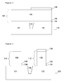
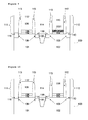
- FIG.1 to FIG.7 and FIG.10 to FIG.11 different process steps for an embodiment of a method of manufacturing a dual work function semiconductor device according to the first aspect of the present invention are described in more detail.
- FIG.8 and FIG.9 an example not forming part of the claimed invention is described.
- FIG.1 illustrates a semiconductor substrate 100, e.g. a silicon substrate.
- the substrate 100 may comprise multiple distinct regions. Most preferably two distinct regions may be defined in the substrate 100, as is illustrated in FIG.1 : a first region 101 and a second region 102.
- the first region 101 may also be referred as the first active region of the device and the second region 102 may also be referred as the second active region of the device.
- the first region 101 and the second region 102 are preferably electrically isolated from each other by an insulating region 103.
- a possible way to isolate the first 101 and second 102 region from each other is by using shallow trench isolation (STI) in between.
- STI shallow trench isolation
- STI is a deep narrow trench, filled with oxide, etched into the semiconductor substrate in between adjacent devices in an integrated circuit to provide electrical isolation between.
- LOC local oxidation of silicon
- a first gate stack will be formed in the first region 101, the first gate stack being for example part of a NMOS transistor (and thus the first region 101 representing a NMOS region for forming a NMOS transistor).
- a second gate stack will be formed in the second region 102, the second gate stack being for example part of a PMOS transistor (and thus the second region 102 representing a PMOS region for forming a PMOS transistor). It should be understood that the invention is not limited thereto and NMOS and PMOS may be interchanged, i.e forming a first PMOS transistor in the first (PMOS) region and a second NMOS transistor in the second (NMOS) region.
- a stack of layers 107 is provided on the semiconductor substrate 100.
- a gate dielectric layer 104 is provided on the substrate ( FIG. 2 ).
- the gate dielectric layer 104 is provided in both the first region 101 and second region 102.
- the gate dielectric layer 104 may be a layer of insulating material, such as for example silicon dioxide (SiO 2 ), silicon nitride (SiN) or silicon oxynitride (Si x O y N 1-x-y ) or more preferably any high-k dielectric material (i.e. k > 3.9) such as for example HfO x , LaO x , TaO x , AlO x , or any combination made thereof.
- the gate dielectric layer 104 may be formed by thermal oxidation, atomic layer deposition (ALD) or chemical vapor deposition (CVD) or physical vapor deposition (PVD), or any other suitable method known to a person skilled in the art.
- the gate dielectric layer 104 may comprise a stack of dielectric materials, such as for example a dielectric capping layer formed on top of a high-k material (e.g. HfO 2 ) formed on top of an (optional) interfacial dielectric layer (e.g. SiO 2 - not shown) between the substrate 100 and high-k material.
- the gate dielectric layer 104 has a thickness preferably in the range of 0.5 nm to 4 nm, leading to an EOT (equivalent oxide thickness) preferably below 2 nm.
- Materials of interest for the metal layer 105 are any oxygen deficient midgap metal such as for example TiN, TaN, TaC, TiC, Ti, Mo and W. With oxygen deficient is meant lacking oxygen, thus a metal containing limited amount to no oxygen atoms.
- the metal should comprise an oxygen concentration below 20 percent mole composition, more preferably below 10 percent mole composition.
- a gate filling material 106 is formed on and in contact with the metal layer 105 ( FIG.2 ).
- gate filling material is meant that the gate filling material serves mainly for further filling up the gate stack.
- the gate filling material may comprise any material suitable for filling up the gate stack to a predefined height. In furthers steps according to embodiments of the present invention the gate filling material may be removed.
- the thickness of the gate filling layer 106 is typically larger than the thickness of the metal layer 105, since the gate filling layer is for further filling up the gate stack.
- the thickness of the gate filling layer 106 is preferably in the range of 50 nm to 200 nm, more preferably in the range of 50 nm to 150 nm.
- the thickness of the gate filling layer 106 is at least 25 times larger than the thickness of the metal layer 105 (for example a 4 nm metal layer with a 100 nm gate filling layer). More preferably the thickness of the gate layer 106 is at least 50 times larger than the thickness of the metal layer 105 (for example a 2 nm metal layer with a 150 nm gate filling layer).
- the gate filling material may (but not necessarily) comprise a work function tuning material.
- the gate filling material may also be a semiconductor material such as for example Si or SiGe. For example a 100 nm poly-Si layer may be formed on top of a 2 nm TiN layer. Alternatively the gate filling material may be a metal such as for example W.
- the gate filling material may be formed with any gate deposition technique well known for a person skilled in the art such as CVD, PVD, ALD or MOCVD.
- the metal layer 105 is a TiN layer. If the TiN layer is capped with N-type Si, which serves as the gate filling layer 106, depending on the thickness of the TiN layer the effective work function may be tuned to a low work function or a midgap work function. For a thin TiN layer, i.e. a thickness in between 0.5 nm to 5 nm, the effective work function can be tuned to an effective work function suitable for a NMOS transistor (i.e. approximately 4.1 eV (+/-0.4 eV)). For a thicker TiN layer, i.e. a thickness above 5 nm, the effective work function can be tuned to a midgap work function (i.e.
- the effective work function of the gate stack may be further tuned to a lower or higher work function value.
- a protective layer 108 may be formed on and in contact with the gate filling layer 106 in the second region 102 ( FIG. 3 ).
- the first 111 and second 112 gate stack may be formed.
- a first and second gate stack may be patterned ( FIG. 4 ).
- a protective layer 108 may be formed on top of the gate filling layer 106 in the second region 102 ( FIG.3 ).
- the protective layer 108 may for example be a SiN layer or a hardmask. This protective layer 108 will protect the second gate stack 112 during further processing steps, more specifically during a following silicidation step, such that the gate filling material of the second gate stack is not silicided.
- This protective layer should be sufficiently thick, i.e. preferably between 20 nm to 300 nm. This is required during further processing steps, as will be explained later.
- the first gate stack and the second gate stack are formed by patterning the protective layer 108, the gate filling layer 106, the metal layer 105 and the gate dielectric layer 104 using conventional lithographic processes and etch processes known for a person skilled in the art.
- spacers 113 are provided. Following the conventional dopants implantation steps, an activation step of the source/drain regions 109 (extension regions/junction regions) and an additional silicidation step in the first region 101 and in the second region 102 are performed thus forming silicide regions 110 ( FIG. 5 ).
- an activation step of the source/drain regions 109 (extension regions/junction regions) and an additional silicidation step in the first region 101 and in the second region 102 are performed thus forming silicide regions 110 ( FIG. 5 ).
- the silicidation step also part of the gate filing material 106 of the first gate stack 111 is silicided (thus forming a first gate silicide region 1101). Due to the protective layer 108 on top of the second gate stack 112 the gate filling material 106 of the second gate stack is not silicided during this silicidation step.
- the protective layer 108 is protecting the top of gate filling material 106 of the second gate stack from being modified into a silicide
- the spacers 113 preferably comprise an insulating material such as for example silicon dioxide (SiO 2 ), silicon nitride (SiN) or silicon oxynitride (SiON). Spacers may be deposited by ALD or CVD and patterned by anisotropic etching, or any other suitable method known to a person skilled in the art.
- This annealing process comprises a high temperature process. This is a high thermal budget process.
- the temperature of the annealing process is typically higher than 500 degrees Celsius, preferably higher than 800 degrees Celsius, more preferably in the range of 800 degrees Celsius to 1400 degrees Celsius. Spike annealing or rapid thermal annealing (RTA) or laser annealing may be used.
- a dielectric layer 114 is formed in the first 101 and the second 102 region at least next to the first 111 and the second 112 gate stack ( FIG. 6 ).
- the dielectric material 114 is thus located adjacent to the first 111 and the second 112 gate stack.
- the dielectric layer is in contact with the sides of the first 111 and the second 112 gate stack.
- the first 111 and the second 112 gate stack may already comprise spacers. If spacers are available, the dielectric layer 114 is in contact with and next to the spacers.
- the dielectric layer 114 may also be present on top of the first gate stack 111, more specifically on top of the gate silicide region 1101 of the first gate stack 111.
- the formation of the dielectric layer 114 may be done for example by depositing the dielectric layer 114 using CVD, followed by polishing back (e.g. using CMP) or etching back the dielectric layer 114 to expose the protective layer 108 in the second region 102. Since the height of the protective layer 108 is sufficiently thick, it will be first exposed during the polishing back (e.g. using CMP) or etching back the dielectric layer 114 process. Otherwise said the thickness of the protective layer 108 is chosen such that during the formation of the dielectric layer 114 more specifically during polishing back the dielectric layer 114, the protective layer 108 is exposed whereas the silicide region 1101 in the first gate stack remains covered by the dielectric layer 114.
- the dielectric layer 114 forms another protective layer for protecting the underlying source/drain regions 109 and silicide regions 110, 1101 and spacers 113 during a subsequent etching process for removing the gate filling material 106 of the second gate stack 112.
- the dielectric layer 114 may comprise for example a low-k dielectric or SiO 2 .
- the dielectric layer 114 may be polished back until the gate silicide region 1101 is exposed. However this is not desirable, since during a next oxidation step, the gate silicide region 1101 will be subjected to the oxidation and will thus partly be oxidized. Advantageously the gate silicide region 1101 is covered by the dielectric layer 114.
- a removal of the protective layer 108 and the gate filling layer 106 of the second gate stack 112 in the second region 102 is performed ( FIG. 7 ).
- the removal step may be done using at least one etching step which does not affect the dielectric layer 114 and the spacers 113.
- the removal step should be selective towards the metal layer 105. If for example SiN is chosen as the protective layer 108, it may be removed with for example a H 3 PO 4 based wet etching process (selective towards the dielectric layer 114, for example SiO 2 ).
- the gate filling layer 106 comprises Si and the metal layer 105 comprises TiN
- this Si gate filling layer may be removed without significantly attacking the TiN layer underneath by a NH 4 OH based wet etch process. After removing the protective layer 108 and the gate filling layer 106 of the second gate stack 112 the metal layer 105 is exposed.
- the exposed metal layer 105 is converted and thus modified into an metal oxide layer 1051 ( FIG.8 ).
- Converting the exposed metal layer 105 into a metal oxide layer 1051 may be done using different techniques. The converting step is performed locally, i.e. only affecting the exposed metal layer 105 of the second gate stack and not affecting the first gate stack.
- the dielectric layer 114 protects the other layers and materials (source/drain 109 and silicide regions 110, 1101, spacers 113, the first gate stack 111) from being modified during the step of converting the metal layer 105 into a metal oxide layer 1051.
- the converting step may be an oxidation step.
- the metal oxide layer 1051 is thus an oxidized metal layer.
- the oxidation step is performed using an annealing step or by implantation of oxygen into the metal layer 105.
- the temperature of the annealing is preferably between 20 degrees Celsius to 500 degrees Celsius, more preferably between 200 degrees Celsius to 400 degrees Celsius.
- the annealing time is preferably above 1 second, more preferably between 10 seconds to 1200 seconds.
- the implantation of oxygen is preferably to be performed with plasma implantation to reduce the penetration of the oxygen species through the thin oxidized metal 1051 layer.
- the metal layer 105 must be completely oxidized, otherwise said, the metal layer 105 must be completely converted into an oxidized metal layer 1051.
- the thickness of the metal layer 105 should thus be chosen such that not only the surface of the metal layer 105 is oxidized but also the bulk of the metal layer 105 is oxidized. In this way, the effective work function of the second gate stack can be modified effectively.
- the material of the metal layer 105 must be chosen such that the effective work function of the second gate stack is tuned towards an effective work function suitable for the second gate stack after the oxidation step.
- the second region may for example be a PMOS region.
- the effective work function of the second (PMOS) region may be tuned towards a suitable effective work function of approximately 5.2 eV ((+/-0.4 eV)) by oxidizing the TiN layer and thus converting the TiN layer into a TiO x N y layer.
- the second gate stack is reformed using another gate filling material.
- the another gate filling material is formed on top of the metal oxide layer 1051. With reformed is meant that at least another gate filling material is formed on top of the metal oxide layer until the final height of the second gate stack is achieved.
- the opening of the second gate stack 112 which was created by removing the protective layer 108 and gate filling material 106 is thus refilled with another gate filling material 115 ( FIG.9 ) followed by polishing back (e.g. using CMP) or etching back the filling material 115 to expose the dielectric layer 114 and the gate silicide region 1101.
- the another gate filling material may be any metal such as for example TiN, TaN, TaC, TiC, Ti, Mo, Ru and W.
- a first transistor is thus formed comprising a metal layer 105 and the first filling material 106 and thereby having predetermined effective work function
- a second transistor is thus formed comprising the oxidized metal layer 1051 and the second filling material 115 and thereby having another predetermined work function.
- a dual work function semiconductor device may be manufactured.
- the second gate stack 112 is first reformed using another gate filling material 116 after removing the protective layer 108 and the gate filling material 106 but before the step of converting the metal layer 105 into a metal oxide 1051.
- the second gate stack is refilled with the another gate filling material 116 after removing the protective layer 108 and the gate filling material 106 but before the step of convernig the metal layer 105 into a metal oxide layer 1051.
- an oxide-rich metal may be used as the another gate filling material 116 such as for example RuO x , MoO x , WO x .
- a first transistor is thus formed comprising a metal layer 105 and the first filling material 106 and thereby having predetermined effective work function
- a second transistor is thus formed comprising the metal oxide layer 1051 and the second filling material 116 and thereby having another predetermined work function.
- a dual work function semiconductor device may be manufactured.
- the effective work function will not change significantly nor will the EOT increase significantly during further process steps in the integration flow.
- the effective work function change is preferably within ⁇ 0.2 eV, even more preferably within ⁇ 0.1 eV and the EOT change is preferably within ⁇ 0.2 nm, even more preferably ⁇ 0.1 nm.
- a large effective work function difference may be achieved between a first (NMOS) and a second (PMOS) transistor starting from the same metal layer for both transistors without affecting the effective oxide thickness (EOT) of the gate dielectric layer significantly.
- EOT effective oxide thickness
- the effective work function difference between NMOS and PMOS transistor could even be increased by adding other work function tuning elements into the first and the second gate stack as known for a person skilled in the art.
- an AlO capping layer may be used in between the gate dielectric layer and the oxidized metal layer to further increase the effective work function of the PMOS transistor towards values of approximately 5.0 eV.
- As I/I one can further lower the effective work function of the NMOS transistor towards values of approximately 4.1 eV.
- the gate dielectric 114 is not exposed to any etching process since it is always protected by the metal layer on top of it. This is especially important to keep the properties of the gate dielectric unchanged and achieve high reliability.
- FIG 12 experimental data are shown for a PMOS transistor according to embodiments.
- C-V curves are shown for a gate stack comprising a TiN metal layer according to embodiments of the present invention.
- a dielectric layer is formed on top of the Si substrate, more specifically a 1nm SiO 2 /2.5nm HfO 2 layer.
- a metal layer more specifically a 2nm TiN layer is formed on top of the gate dielectric layer.
- a poly-Si gate filling material was formed on top of the TiN layer. After junction activation anneal and silicidation, the poly-Si gate filling material is selectively removed with ammonia. The TiN layer is thus exposed after the removal step.
- an O 2 anneal was performed at 300 degrees Celsius for 1 (diamonds) to 4 (dots) minutes (a reference without (squares) this anneal is also shown).
- the TiN layer is thus converted into a TiON layer after the oxidation step.
- the gate stack was refilled with a gate filling material, in this example a 50nm TiN capping layer.
- a 420 degrees Celsius forming gas anneal was performed for 20 minutes to passivate the dielectrics, a commonly known process for a person skilled in the art with the purpose of achieving low defect density in the gate dielectric. From the electric measurements on a capacitor device formed with this gate stack, i.e.
- FIG 14 experimental data (C-V curves) are shown for an analogous PMOS transistor gate stack as in figure 12 .
- the O 2 anneal was performed before the junction activation step. More precisely first a dielectric layer is formed on top of the Si substrate, more specifically a 1nm SiO 2 /2.5nm HfO 2 layer. Next a metal layer, more specifically a 2nm TiN layer is formed on top of the gate dielectric layer. Immediately after the 2 nm TiN deposition an O 2 anneal was performed at 300 degrees Celsius for 1 (dots) to 4 (rectangles) minutes (a reference without (squares) this anneal is also shown).
- a 100 nm poly-Si gate filling material was formed by using CVD on top of the TiN layer. Thereafter, according to prior art, a high temperature junction activation anneal is performed. It is found that the EOT (equivalent oxide thickness) is increased by 0.48 nm. The effective work function of the gate stack is not significantly impacted. This increase in EOT is however not desired and is due to the junction activation step which is performed after the oxygen anneal of the metal TiN layer.
- FIG 13 experimental data are shown for an NMOS transistor according to embodiments of the present invention.
- a C-V curve is shown for a gate stack comprising a TiN metal layer according to embodiments of the present invention.
- a dielectric layer is formed on top of the Si substrate, more specifically a 1nm SiO 2 /2.5nm HfO 2 layer.
- a metal layer more specifically a 2nm TiN layer is formed on top of the gate dielectric layer.
- a poly-Si gate filling material was formed on top of the TiN layer. From the electric measurements on a capacitor device formed with this gate stack, i.e. the C-V curves, it is seen that the effective work function for the NMOS transistor is approximately 4.4 eV, which is in the range of the desired work function of approximately 4.1 eV (+/-0.4 eV) for an NMOS transistor.
- the dual work function semiconductor device comprises a semiconductor substrate; a first gate stack and a second gate stack on the semiconductor substrate.
- the first gate stack comprises a first gate dielectric layer on and in contact with the semiconductor substrate; a metal layer on and in contact with the first gate dielectric layer; a gate filling material on and in contact with the metal layer.
- the second gate stack comprises a second gate dielectric layer on and in contact with the semiconductor substrate, the second gate dielectric layer consisting of the same material as the first gate dielectric layer; a metal oxide layer on and in contact with the first gate dielectric layer; another gate filling material on and in contact with the metal oxide layer, the another gate filling material comprising another material than the gate filling material from the first gate stack.
- the metal oxide layer comprises a metal oxide formed by converting a metal into the metal oxide, the metal being the same as the metal from the metal layer in the first gate stack.
- the metal layer of the first gate stack is for example M.
- the metal oxide layer of the second gate stack will then be M x O y .
- the gate filling material of the first gate stack comprises preferably Si or SiGe.
- the metal layer of the first gate stack comprises preferably a midgap oxygen-deficient metal, such as for example TiN, TaN, TaC, TiC, Ti, Mo, Ru or W.
Landscapes
- Metal-Oxide And Bipolar Metal-Oxide Semiconductor Integrated Circuits (AREA)
- Electrodes Of Semiconductors (AREA)
- Insulated Gate Type Field-Effect Transistor (AREA)
Claims (6)
- Verfahren zur Herstellung eines Halbleiterbauelementes mit dualer Austrittsarbeit, wobei das Verfahren umfasst:- Bereitstellen eines Halbleitersubstrats (100);- Bereitstellen einer Gate-dielektrischen Schicht (104) auf und in Kontakt mit dem Halbleitersubstrat (100);- Bilden einer Metallschicht (105), die eine Dicke aufweist, auf und in Kontakt mit der Gate-dielektrischen Schicht (104);- Bilden einer Schicht aus Gate-Füllmaterial (106) auf und in Kontakt mit der Metallschicht (105);- Strukturieren der Gate-dielektrischen Schicht (104), der Metallschicht (105) und der Gate-Füllungsschicht (106), um einen ersten Gate-Stack (111) und einen zweiten Gate-Stack (112) zu bilden;- einen Ausheilungsschritt nach dem Strukturierungsschritt, dabei Herausbilden aktivierter Source- und Drain-Gebiete (109) in dem Halbleitersubstrat (100) für sowohl den ersten Gate-Stack (111) als auch den zweiten Gate-Stack (112);- nach dem Ausheilungsschritt, selektives Entfernen des Gate-Füllmaterials (106) von nur dem zweiten Gate-Stack (112), dabei Freilegen der darunterliegenden Metallschicht (105),- nach dem Entfernen des Gate-Füllmaterials (106), Zurückbilden des zweiten Gate-Stacks mit einem anderen Gate-Füllmaterial (116), wobei das andere Gate-Füllmaterial ein sauerstoffreiches Metall umfasst;- Durchführen einer Wärmebehandlung des zweiten Gate-Stacks, dabei Liefern von Sauerstoff aus dem anderen Gate-Füllmaterial (116) in die Metallschicht (105) und Umwandeln der Metallschicht (105) in eine Metalloxidschicht (1051).
- Verfahren zur Herstellung eines Halbleiterbauelementes mit dualer Austrittsarbeit nach Anspruch 1, wobei die Dicke der Metallschicht (105) ausgewählt ist, um eine effektive Austrittsarbeit ausgewählt für den ersten Gate-Stack und eine andere effektive Austrittsarbeit ausgewählt für den zweiten Gate-Stack nach der Umwandlung der Metallschicht (105), zu erreichen.
- Verfahren zur Herstellung eines Halbleiterbauelementes mit dualer Austrittsarbeit nach einem der Ansprüche 1 oder 2, wobei die Dicke der Metallschicht (105) in dem Bereich von 0,5 Nanometer bis 5 Nanometer liegt.
- Verfahren zur Herstellung eines Halbleiterbauelementes mit dualer Austrittsarbeit nach einem der Ansprüche 1 bis 3, wobei die Metallschicht (105) ein sauerstoffarmes Metall umfasst.
- Verfahren zur Herstellung eines Halbleiterbauelementes mit dualer Austrittsarbeit nach einem der Ansprüche 1 bis 4, wobei das Gate-Füllmaterial (106) aus Si oder SiGe ausgewählt wird.
- Verfahren zur Herstellung eines Halbleiterbauelementes mit dualer Austrittsarbeit nach einem der Ansprüche 1 bis 5, wobei das andere Gate-Füllmaterial (116) jedes von MoOx, RuOx or WOx umfasst.
Applications Claiming Priority (2)
| Application Number | Priority Date | Filing Date | Title |
|---|---|---|---|
| US10536808P | 2008-10-14 | 2008-10-14 | |
| EP09075085A EP2197028A1 (de) | 2008-10-14 | 2009-02-25 | Verfahren zur Herstellung eines Halbleiterelements mit dualer Austrittsarbeit und das damit gefertigte Element |
Related Parent Applications (2)
| Application Number | Title | Priority Date | Filing Date |
|---|---|---|---|
| EP09075085.2 Division | 2009-02-25 | ||
| EP09075085A Division EP2197028A1 (de) | 2008-10-14 | 2009-02-25 | Verfahren zur Herstellung eines Halbleiterelements mit dualer Austrittsarbeit und das damit gefertigte Element |
Publications (2)
| Publication Number | Publication Date |
|---|---|
| EP2584601A1 EP2584601A1 (de) | 2013-04-24 |
| EP2584601B1 true EP2584601B1 (de) | 2015-08-19 |
Family
ID=41510798
Family Applications (2)
| Application Number | Title | Priority Date | Filing Date |
|---|---|---|---|
| EP09075085A Ceased EP2197028A1 (de) | 2008-10-14 | 2009-02-25 | Verfahren zur Herstellung eines Halbleiterelements mit dualer Austrittsarbeit und das damit gefertigte Element |
| EP13152000.9A Active EP2584601B1 (de) | 2008-10-14 | 2009-02-25 | Verfahren zur Herstellung einer Halbleitervorrichtung mit dualer Austrittsarbeit |
Family Applications Before (1)
| Application Number | Title | Priority Date | Filing Date |
|---|---|---|---|
| EP09075085A Ceased EP2197028A1 (de) | 2008-10-14 | 2009-02-25 | Verfahren zur Herstellung eines Halbleiterelements mit dualer Austrittsarbeit und das damit gefertigte Element |
Country Status (2)
| Country | Link |
|---|---|
| EP (2) | EP2197028A1 (de) |
| JP (1) | JP5469988B2 (de) |
Families Citing this family (7)
| Publication number | Priority date | Publication date | Assignee | Title |
|---|---|---|---|---|
| CN102122637B (zh) * | 2010-01-08 | 2013-09-11 | 中芯国际集成电路制造(上海)有限公司 | 检测结构、检测方法及形成检测结构的方法 |
| WO2012086102A1 (ja) * | 2010-12-24 | 2012-06-28 | パナソニック株式会社 | 半導体装置及びその製造方法 |
| KR102084657B1 (ko) * | 2013-11-04 | 2020-03-04 | 에스케이하이닉스 주식회사 | 트랜지스터의 문턱전압조절을 위한 방법 및 게이트구조물 |
| DE102018122654A1 (de) * | 2017-09-29 | 2019-04-04 | Taiwan Semiconductor Manufacturing Company, Ltd. | Finnenfeldeffekttransistorvorrichtung und verfahren zum bilden derselben |
| US10504782B2 (en) | 2017-09-29 | 2019-12-10 | Taiwan Semiconductor Manufacturing Company, Ltd. | Fin Field-Effect Transistor device and method of forming the same |
| JP6957310B2 (ja) * | 2017-10-24 | 2021-11-02 | 東京エレクトロン株式会社 | 半導体装置およびcmosトランジスタ |
| CN109904233B (zh) * | 2019-02-02 | 2022-04-26 | 中国科学院微电子研究所 | 金属栅功函数的调节方法及mosfet的制备方法 |
Family Cites Families (10)
| Publication number | Priority date | Publication date | Assignee | Title |
|---|---|---|---|---|
| US6458695B1 (en) * | 2001-10-18 | 2002-10-01 | Chartered Semiconductor Manufacturing Ltd. | Methods to form dual metal gates by incorporating metals and their conductive oxides |
| JP2003273350A (ja) * | 2002-03-15 | 2003-09-26 | Nec Corp | 半導体装置及びその製造方法 |
| US7045406B2 (en) * | 2002-12-03 | 2006-05-16 | Asm International, N.V. | Method of forming an electrode with adjusted work function |
| US7122414B2 (en) * | 2002-12-03 | 2006-10-17 | Asm International, Inc. | Method to fabricate dual metal CMOS devices |
| JP4091530B2 (ja) * | 2003-07-25 | 2008-05-28 | 株式会社東芝 | 半導体装置の製造方法 |
| KR20070045268A (ko) * | 2004-08-24 | 2007-05-02 | 코닌클리즈케 필립스 일렉트로닉스 엔.브이. | 반도체 디바이스 및 그 제조 방법 |
| JP2006060173A (ja) * | 2004-08-24 | 2006-03-02 | Matsushita Electric Ind Co Ltd | 半導体装置及びその製造方法 |
| JP4455427B2 (ja) * | 2005-06-29 | 2010-04-21 | 株式会社東芝 | 半導体装置及びその製造方法 |
| GB0625004D0 (en) * | 2006-12-15 | 2007-01-24 | Nxp Bv | Semiconductor device and method of manufacture |
| US7812414B2 (en) * | 2007-01-23 | 2010-10-12 | Taiwan Semiconductor Manufacturing Company, Ltd. | Hybrid process for forming metal gates |
-
2009
- 2009-02-25 EP EP09075085A patent/EP2197028A1/de not_active Ceased
- 2009-02-25 EP EP13152000.9A patent/EP2584601B1/de active Active
- 2009-10-14 JP JP2009237222A patent/JP5469988B2/ja active Active
Also Published As
| Publication number | Publication date |
|---|---|
| EP2197028A1 (de) | 2010-06-16 |
| EP2584601A1 (de) | 2013-04-24 |
| JP5469988B2 (ja) | 2014-04-16 |
| JP2010114436A (ja) | 2010-05-20 |
Similar Documents
| Publication | Publication Date | Title |
|---|---|---|
| US9024299B2 (en) | Method for fabricating a dual work function semiconductor device and the device made thereof | |
| US8012827B2 (en) | Method for fabricating a dual workfunction semiconductor device and the device made thereof | |
| US10424517B2 (en) | Method for manufacturing a dual work function semiconductor device and the semiconductor device made thereof | |
| US9397009B2 (en) | Structure and method for metal gate stack oxygen concentration control using an oxygen diffusion barrier layer and a sacrificial oxygen gettering layer | |
| EP2112687B1 (de) | Verfahren zur Herstellung eines Halbleiterebaulements mit dualer Austrittsarbeit-Funktion und das damit gefertigte Element | |
| US8658489B2 (en) | Method for dual work function metal gate CMOS with selective capping | |
| US8525263B2 (en) | Programmable high-k/metal gate memory device | |
| JP5569173B2 (ja) | 半導体装置の製造方法及び半導体装置 | |
| KR101521948B1 (ko) | 반도체 장치 및 그 제조 방법 | |
| US7855134B2 (en) | Semiconductor device and manufacturing method of the same | |
| CN101427386A (zh) | 阻挡层的选择性实施以实现在具有高k电介质的CMOS器件制造中的阈值电压控制 | |
| EP2584601B1 (de) | Verfahren zur Herstellung einer Halbleitervorrichtung mit dualer Austrittsarbeit | |
| US20120256270A1 (en) | Dual metal gates using one metal to alter work function of another metal | |
| CN103354238A (zh) | 半导体器件 | |
| JP2013004968A (ja) | 半導体装置とその製造方法 | |
| US20090057786A1 (en) | Semiconductor device and method of manufacturing semiconductor device | |
| JP5056418B2 (ja) | 半導体装置およびその製造方法 |
Legal Events
| Date | Code | Title | Description |
|---|---|---|---|
| PUAI | Public reference made under article 153(3) epc to a published international application that has entered the european phase |
Free format text: ORIGINAL CODE: 0009012 |
|
| 17P | Request for examination filed |
Effective date: 20130121 |
|
| AC | Divisional application: reference to earlier application |
Ref document number: 2197028 Country of ref document: EP Kind code of ref document: P |
|
| AK | Designated contracting states |
Kind code of ref document: A1 Designated state(s): AT BE BG CH CY CZ DE DK EE ES FI FR GB GR HR HU IE IS IT LI LT LU LV MC MK MT NL NO PL PT RO SE SI SK TR |
|
| AX | Request for extension of the european patent |
Extension state: AL BA RS |
|
| RBV | Designated contracting states (corrected) |
Designated state(s): AT BE BG CH CY CZ DE DK EE ES FI FR GB GR HR HU IE IS IT LI LT LU LV MC MK MT NL NO PL PT RO SE SI SK TR |
|
| 17Q | First examination report despatched |
Effective date: 20140116 |
|
| GRAP | Despatch of communication of intention to grant a patent |
Free format text: ORIGINAL CODE: EPIDOSNIGR1 |
|
| INTG | Intention to grant announced |
Effective date: 20150506 |
|
| GRAS | Grant fee paid |
Free format text: ORIGINAL CODE: EPIDOSNIGR3 |
|
| GRAA | (expected) grant |
Free format text: ORIGINAL CODE: 0009210 |
|
| AC | Divisional application: reference to earlier application |
Ref document number: 2197028 Country of ref document: EP Kind code of ref document: P |
|
| AK | Designated contracting states |
Kind code of ref document: B1 Designated state(s): AT BE BG CH CY CZ DE DK EE ES FI FR GB GR HR HU IE IS IT LI LT LU LV MC MK MT NL NO PL PT RO SE SI SK TR |
|
| REG | Reference to a national code |
Ref country code: GB Ref legal event code: FG4D |
|
| REG | Reference to a national code |
Ref country code: CH Ref legal event code: EP |
|
| REG | Reference to a national code |
Ref country code: IE Ref legal event code: FG4D |
|
| REG | Reference to a national code |
Ref country code: AT Ref legal event code: REF Ref document number: 744335 Country of ref document: AT Kind code of ref document: T Effective date: 20150915 |
|
| REG | Reference to a national code |
Ref country code: DE Ref legal event code: R096 Ref document number: 602009033112 Country of ref document: DE |
|
| REG | Reference to a national code |
Ref country code: AT Ref legal event code: MK05 Ref document number: 744335 Country of ref document: AT Kind code of ref document: T Effective date: 20150819 |
|
| REG | Reference to a national code |
Ref country code: FR Ref legal event code: PLFP Year of fee payment: 8 |
|
| REG | Reference to a national code |
Ref country code: LT Ref legal event code: MG4D |
|
| REG | Reference to a national code |
Ref country code: NL Ref legal event code: MP Effective date: 20150819 |
|
| PG25 | Lapsed in a contracting state [announced via postgrant information from national office to epo] |
Ref country code: LT Free format text: LAPSE BECAUSE OF FAILURE TO SUBMIT A TRANSLATION OF THE DESCRIPTION OR TO PAY THE FEE WITHIN THE PRESCRIBED TIME-LIMIT Effective date: 20150819 Ref country code: NO Free format text: LAPSE BECAUSE OF FAILURE TO SUBMIT A TRANSLATION OF THE DESCRIPTION OR TO PAY THE FEE WITHIN THE PRESCRIBED TIME-LIMIT Effective date: 20151119 Ref country code: FI Free format text: LAPSE BECAUSE OF FAILURE TO SUBMIT A TRANSLATION OF THE DESCRIPTION OR TO PAY THE FEE WITHIN THE PRESCRIBED TIME-LIMIT Effective date: 20150819 Ref country code: LV Free format text: LAPSE BECAUSE OF FAILURE TO SUBMIT A TRANSLATION OF THE DESCRIPTION OR TO PAY THE FEE WITHIN THE PRESCRIBED TIME-LIMIT Effective date: 20150819 Ref country code: GR Free format text: LAPSE BECAUSE OF FAILURE TO SUBMIT A TRANSLATION OF THE DESCRIPTION OR TO PAY THE FEE WITHIN THE PRESCRIBED TIME-LIMIT Effective date: 20151120 |
|
| PG25 | Lapsed in a contracting state [announced via postgrant information from national office to epo] |
Ref country code: PL Free format text: LAPSE BECAUSE OF FAILURE TO SUBMIT A TRANSLATION OF THE DESCRIPTION OR TO PAY THE FEE WITHIN THE PRESCRIBED TIME-LIMIT Effective date: 20150819 Ref country code: SE Free format text: LAPSE BECAUSE OF FAILURE TO SUBMIT A TRANSLATION OF THE DESCRIPTION OR TO PAY THE FEE WITHIN THE PRESCRIBED TIME-LIMIT Effective date: 20150819 Ref country code: ES Free format text: LAPSE BECAUSE OF FAILURE TO SUBMIT A TRANSLATION OF THE DESCRIPTION OR TO PAY THE FEE WITHIN THE PRESCRIBED TIME-LIMIT Effective date: 20150819 Ref country code: AT Free format text: LAPSE BECAUSE OF FAILURE TO SUBMIT A TRANSLATION OF THE DESCRIPTION OR TO PAY THE FEE WITHIN THE PRESCRIBED TIME-LIMIT Effective date: 20150819 Ref country code: IS Free format text: LAPSE BECAUSE OF FAILURE TO SUBMIT A TRANSLATION OF THE DESCRIPTION OR TO PAY THE FEE WITHIN THE PRESCRIBED TIME-LIMIT Effective date: 20151219 Ref country code: PT Free format text: LAPSE BECAUSE OF FAILURE TO SUBMIT A TRANSLATION OF THE DESCRIPTION OR TO PAY THE FEE WITHIN THE PRESCRIBED TIME-LIMIT Effective date: 20151221 |
|
| PG25 | Lapsed in a contracting state [announced via postgrant information from national office to epo] |
Ref country code: NL Free format text: LAPSE BECAUSE OF FAILURE TO SUBMIT A TRANSLATION OF THE DESCRIPTION OR TO PAY THE FEE WITHIN THE PRESCRIBED TIME-LIMIT Effective date: 20150819 |
|
| PG25 | Lapsed in a contracting state [announced via postgrant information from national office to epo] |
Ref country code: CZ Free format text: LAPSE BECAUSE OF FAILURE TO SUBMIT A TRANSLATION OF THE DESCRIPTION OR TO PAY THE FEE WITHIN THE PRESCRIBED TIME-LIMIT Effective date: 20150819 Ref country code: DK Free format text: LAPSE BECAUSE OF FAILURE TO SUBMIT A TRANSLATION OF THE DESCRIPTION OR TO PAY THE FEE WITHIN THE PRESCRIBED TIME-LIMIT Effective date: 20150819 Ref country code: SK Free format text: LAPSE BECAUSE OF FAILURE TO SUBMIT A TRANSLATION OF THE DESCRIPTION OR TO PAY THE FEE WITHIN THE PRESCRIBED TIME-LIMIT Effective date: 20150819 Ref country code: IT Free format text: LAPSE BECAUSE OF FAILURE TO SUBMIT A TRANSLATION OF THE DESCRIPTION OR TO PAY THE FEE WITHIN THE PRESCRIBED TIME-LIMIT Effective date: 20150819 Ref country code: EE Free format text: LAPSE BECAUSE OF FAILURE TO SUBMIT A TRANSLATION OF THE DESCRIPTION OR TO PAY THE FEE WITHIN THE PRESCRIBED TIME-LIMIT Effective date: 20150819 |
|
| REG | Reference to a national code |
Ref country code: DE Ref legal event code: R097 Ref document number: 602009033112 Country of ref document: DE |
|
| PG25 | Lapsed in a contracting state [announced via postgrant information from national office to epo] |
Ref country code: RO Free format text: LAPSE BECAUSE OF FAILURE TO SUBMIT A TRANSLATION OF THE DESCRIPTION OR TO PAY THE FEE WITHIN THE PRESCRIBED TIME-LIMIT Effective date: 20150819 Ref country code: BE Free format text: LAPSE BECAUSE OF NON-PAYMENT OF DUE FEES Effective date: 20160229 |
|
| PLBE | No opposition filed within time limit |
Free format text: ORIGINAL CODE: 0009261 |
|
| STAA | Information on the status of an ep patent application or granted ep patent |
Free format text: STATUS: NO OPPOSITION FILED WITHIN TIME LIMIT |
|
| 26N | No opposition filed |
Effective date: 20160520 |
|
| PG25 | Lapsed in a contracting state [announced via postgrant information from national office to epo] |
Ref country code: SI Free format text: LAPSE BECAUSE OF FAILURE TO SUBMIT A TRANSLATION OF THE DESCRIPTION OR TO PAY THE FEE WITHIN THE PRESCRIBED TIME-LIMIT Effective date: 20150819 |
|
| PG25 | Lapsed in a contracting state [announced via postgrant information from national office to epo] |
Ref country code: LU Free format text: LAPSE BECAUSE OF FAILURE TO SUBMIT A TRANSLATION OF THE DESCRIPTION OR TO PAY THE FEE WITHIN THE PRESCRIBED TIME-LIMIT Effective date: 20160225 Ref country code: MC Free format text: LAPSE BECAUSE OF FAILURE TO SUBMIT A TRANSLATION OF THE DESCRIPTION OR TO PAY THE FEE WITHIN THE PRESCRIBED TIME-LIMIT Effective date: 20150819 |
|
| REG | Reference to a national code |
Ref country code: CH Ref legal event code: PL |
|
| GBPC | Gb: european patent ceased through non-payment of renewal fee |
Effective date: 20160225 |
|
| PG25 | Lapsed in a contracting state [announced via postgrant information from national office to epo] |
Ref country code: LI Free format text: LAPSE BECAUSE OF NON-PAYMENT OF DUE FEES Effective date: 20160229 Ref country code: CH Free format text: LAPSE BECAUSE OF NON-PAYMENT OF DUE FEES Effective date: 20160229 |
|
| REG | Reference to a national code |
Ref country code: IE Ref legal event code: MM4A |
|
| PG25 | Lapsed in a contracting state [announced via postgrant information from national office to epo] |
Ref country code: BE Free format text: LAPSE BECAUSE OF FAILURE TO SUBMIT A TRANSLATION OF THE DESCRIPTION OR TO PAY THE FEE WITHIN THE PRESCRIBED TIME-LIMIT Effective date: 20150819 |
|
| REG | Reference to a national code |
Ref country code: FR Ref legal event code: PLFP Year of fee payment: 9 |
|
| PG25 | Lapsed in a contracting state [announced via postgrant information from national office to epo] |
Ref country code: IE Free format text: LAPSE BECAUSE OF NON-PAYMENT OF DUE FEES Effective date: 20160225 Ref country code: GB Free format text: LAPSE BECAUSE OF NON-PAYMENT OF DUE FEES Effective date: 20160225 |
|
| PG25 | Lapsed in a contracting state [announced via postgrant information from national office to epo] |
Ref country code: MT Free format text: LAPSE BECAUSE OF FAILURE TO SUBMIT A TRANSLATION OF THE DESCRIPTION OR TO PAY THE FEE WITHIN THE PRESCRIBED TIME-LIMIT Effective date: 20150819 |
|
| REG | Reference to a national code |
Ref country code: FR Ref legal event code: PLFP Year of fee payment: 10 |
|
| PG25 | Lapsed in a contracting state [announced via postgrant information from national office to epo] |
Ref country code: CY Free format text: LAPSE BECAUSE OF FAILURE TO SUBMIT A TRANSLATION OF THE DESCRIPTION OR TO PAY THE FEE WITHIN THE PRESCRIBED TIME-LIMIT Effective date: 20150819 Ref country code: HU Free format text: LAPSE BECAUSE OF FAILURE TO SUBMIT A TRANSLATION OF THE DESCRIPTION OR TO PAY THE FEE WITHIN THE PRESCRIBED TIME-LIMIT; INVALID AB INITIO Effective date: 20090225 |
|
| PG25 | Lapsed in a contracting state [announced via postgrant information from national office to epo] |
Ref country code: HR Free format text: LAPSE BECAUSE OF FAILURE TO SUBMIT A TRANSLATION OF THE DESCRIPTION OR TO PAY THE FEE WITHIN THE PRESCRIBED TIME-LIMIT Effective date: 20150819 Ref country code: MK Free format text: LAPSE BECAUSE OF FAILURE TO SUBMIT A TRANSLATION OF THE DESCRIPTION OR TO PAY THE FEE WITHIN THE PRESCRIBED TIME-LIMIT Effective date: 20150819 Ref country code: TR Free format text: LAPSE BECAUSE OF FAILURE TO SUBMIT A TRANSLATION OF THE DESCRIPTION OR TO PAY THE FEE WITHIN THE PRESCRIBED TIME-LIMIT Effective date: 20150819 Ref country code: MT Free format text: LAPSE BECAUSE OF FAILURE TO SUBMIT A TRANSLATION OF THE DESCRIPTION OR TO PAY THE FEE WITHIN THE PRESCRIBED TIME-LIMIT Effective date: 20160229 |
|
| PG25 | Lapsed in a contracting state [announced via postgrant information from national office to epo] |
Ref country code: BG Free format text: LAPSE BECAUSE OF FAILURE TO SUBMIT A TRANSLATION OF THE DESCRIPTION OR TO PAY THE FEE WITHIN THE PRESCRIBED TIME-LIMIT Effective date: 20150819 |
|
| P01 | Opt-out of the competence of the unified patent court (upc) registered |
Effective date: 20230513 |
|
| REG | Reference to a national code |
Ref country code: DE Ref legal event code: R079 Ref document number: 602009033112 Country of ref document: DE Free format text: PREVIOUS MAIN CLASS: H01L0021823400 Ipc: H10D0084830000 |
|
| PGFP | Annual fee paid to national office [announced via postgrant information from national office to epo] |
Ref country code: DE Payment date: 20260121 Year of fee payment: 18 |
|
| PGFP | Annual fee paid to national office [announced via postgrant information from national office to epo] |
Ref country code: FR Payment date: 20260121 Year of fee payment: 18 |