EP2586064B1 - Procede de texturation d'une surface en silicium pour creer un silicium noir pour des applications photovoltaïques - Google Patents
Procede de texturation d'une surface en silicium pour creer un silicium noir pour des applications photovoltaïques Download PDFInfo
- Publication number
- EP2586064B1 EP2586064B1 EP11754717.4A EP11754717A EP2586064B1 EP 2586064 B1 EP2586064 B1 EP 2586064B1 EP 11754717 A EP11754717 A EP 11754717A EP 2586064 B1 EP2586064 B1 EP 2586064B1
- Authority
- EP
- European Patent Office
- Prior art keywords
- silica
- molten salt
- silicon
- salt electrolyte
- electrical conductor
- Prior art date
- Legal status (The legal status is an assumption and is not a legal conclusion. Google has not performed a legal analysis and makes no representation as to the accuracy of the status listed.)
- Not-in-force
Links
- 229910052710 silicon Inorganic materials 0.000 title claims description 45
- XUIMIQQOPSSXEZ-UHFFFAOYSA-N Silicon Chemical compound [Si] XUIMIQQOPSSXEZ-UHFFFAOYSA-N 0.000 title claims description 44
- 239000010703 silicon Substances 0.000 title claims description 44
- 238000000034 method Methods 0.000 title claims description 31
- 229910021418 black silicon Inorganic materials 0.000 title description 6
- VYPSYNLAJGMNEJ-UHFFFAOYSA-N Silicium dioxide Chemical compound O=[Si]=O VYPSYNLAJGMNEJ-UHFFFAOYSA-N 0.000 claims description 94
- 239000000377 silicon dioxide Substances 0.000 claims description 47
- 150000003839 salts Chemical class 0.000 claims description 26
- 239000003792 electrolyte Substances 0.000 claims description 25
- 239000004020 conductor Substances 0.000 claims description 18
- 239000002344 surface layer Substances 0.000 claims description 18
- 238000000151 deposition Methods 0.000 claims description 15
- 239000000758 substrate Substances 0.000 claims description 12
- 230000008021 deposition Effects 0.000 claims description 11
- 150000001768 cations Chemical class 0.000 claims description 8
- 239000011575 calcium Substances 0.000 claims description 7
- 239000011148 porous material Substances 0.000 claims description 7
- 239000001110 calcium chloride Substances 0.000 claims description 6
- 229910001628 calcium chloride Inorganic materials 0.000 claims description 6
- OYPRJOBELJOOCE-UHFFFAOYSA-N Calcium Chemical compound [Ca] OYPRJOBELJOOCE-UHFFFAOYSA-N 0.000 claims description 5
- ZOKXTWBITQBERF-UHFFFAOYSA-N Molybdenum Chemical group [Mo] ZOKXTWBITQBERF-UHFFFAOYSA-N 0.000 claims description 5
- 229910052791 calcium Inorganic materials 0.000 claims description 5
- 238000000576 coating method Methods 0.000 claims description 5
- 239000000463 material Substances 0.000 claims description 5
- UXVMQQNJUSDDNG-UHFFFAOYSA-L Calcium chloride Chemical group [Cl-].[Cl-].[Ca+2] UXVMQQNJUSDDNG-UHFFFAOYSA-L 0.000 claims description 4
- 239000011248 coating agent Substances 0.000 claims description 4
- WHXSMMKQMYFTQS-UHFFFAOYSA-N Lithium Chemical compound [Li] WHXSMMKQMYFTQS-UHFFFAOYSA-N 0.000 claims description 2
- 229910052788 barium Inorganic materials 0.000 claims description 2
- DSAJWYNOEDNPEQ-UHFFFAOYSA-N barium atom Chemical compound [Ba] DSAJWYNOEDNPEQ-UHFFFAOYSA-N 0.000 claims description 2
- 150000004820 halides Chemical class 0.000 claims description 2
- 229910052744 lithium Inorganic materials 0.000 claims description 2
- 230000008018 melting Effects 0.000 claims description 2
- 238000002844 melting Methods 0.000 claims description 2
- 229910052750 molybdenum Inorganic materials 0.000 claims description 2
- 239000011733 molybdenum Substances 0.000 claims description 2
- 229910052712 strontium Inorganic materials 0.000 claims description 2
- CIOAGBVUUVVLOB-UHFFFAOYSA-N strontium atom Chemical compound [Sr] CIOAGBVUUVVLOB-UHFFFAOYSA-N 0.000 claims description 2
- WFKWXMTUELFFGS-UHFFFAOYSA-N tungsten Chemical compound [W] WFKWXMTUELFFGS-UHFFFAOYSA-N 0.000 claims description 2
- 229910052721 tungsten Inorganic materials 0.000 claims description 2
- 239000010937 tungsten Substances 0.000 claims description 2
- 230000000063 preceeding effect Effects 0.000 claims 2
- 239000010410 layer Substances 0.000 description 14
- 235000012431 wafers Nutrition 0.000 description 12
- OKTJSMMVPCPJKN-UHFFFAOYSA-N Carbon Chemical compound [C] OKTJSMMVPCPJKN-UHFFFAOYSA-N 0.000 description 11
- 229910002804 graphite Inorganic materials 0.000 description 8
- 239000010439 graphite Substances 0.000 description 8
- 229910052681 coesite Inorganic materials 0.000 description 6
- 229910052906 cristobalite Inorganic materials 0.000 description 6
- 230000003635 deoxygenating effect Effects 0.000 description 6
- 238000005868 electrolysis reaction Methods 0.000 description 6
- 239000001301 oxygen Substances 0.000 description 6
- 229910052760 oxygen Inorganic materials 0.000 description 6
- 229910052682 stishovite Inorganic materials 0.000 description 6
- 229910052905 tridymite Inorganic materials 0.000 description 6
- QVGXLLKOCUKJST-UHFFFAOYSA-N atomic oxygen Chemical compound [O] QVGXLLKOCUKJST-UHFFFAOYSA-N 0.000 description 4
- 239000011532 electronic conductor Substances 0.000 description 4
- 238000005530 etching Methods 0.000 description 4
- 239000007789 gas Substances 0.000 description 4
- 239000002243 precursor Substances 0.000 description 4
- UFHFLCQGNIYNRP-UHFFFAOYSA-N Hydrogen Chemical compound [H][H] UFHFLCQGNIYNRP-UHFFFAOYSA-N 0.000 description 3
- 230000015572 biosynthetic process Effects 0.000 description 3
- 229910052799 carbon Inorganic materials 0.000 description 3
- 239000003054 catalyst Substances 0.000 description 3
- 238000005755 formation reaction Methods 0.000 description 3
- 229910052739 hydrogen Inorganic materials 0.000 description 3
- 239000001257 hydrogen Substances 0.000 description 3
- 230000003287 optical effect Effects 0.000 description 3
- 125000004430 oxygen atom Chemical group O* 0.000 description 3
- KRHYYFGTRYWZRS-UHFFFAOYSA-N Fluorane Chemical compound F KRHYYFGTRYWZRS-UHFFFAOYSA-N 0.000 description 2
- GWEVSGVZZGPLCZ-UHFFFAOYSA-N Titan oxide Chemical compound O=[Ti]=O GWEVSGVZZGPLCZ-UHFFFAOYSA-N 0.000 description 2
- 238000006243 chemical reaction Methods 0.000 description 2
- 230000005611 electricity Effects 0.000 description 2
- 230000031700 light absorption Effects 0.000 description 2
- 238000004519 manufacturing process Methods 0.000 description 2
- 238000005259 measurement Methods 0.000 description 2
- -1 oxygen ions Chemical class 0.000 description 2
- 230000010287 polarization Effects 0.000 description 2
- 238000000985 reflectance spectrum Methods 0.000 description 2
- 239000007787 solid Substances 0.000 description 2
- 239000000126 substance Substances 0.000 description 2
- XLYOFNOQVPJJNP-UHFFFAOYSA-N water Substances O XLYOFNOQVPJJNP-UHFFFAOYSA-N 0.000 description 2
- PXELHGDYRQLRQO-UHFFFAOYSA-N 1-butyl-1-methylpyrrolidin-1-ium Chemical compound CCCC[N+]1(C)CCCC1 PXELHGDYRQLRQO-UHFFFAOYSA-N 0.000 description 1
- NJMWOUFKYKNWDW-UHFFFAOYSA-N 1-ethyl-3-methylimidazolium Chemical compound CCN1C=C[N+](C)=C1 NJMWOUFKYKNWDW-UHFFFAOYSA-N 0.000 description 1
- UGFAIRIUMAVXCW-UHFFFAOYSA-N Carbon monoxide Chemical compound [O+]#[C-] UGFAIRIUMAVXCW-UHFFFAOYSA-N 0.000 description 1
- XOJVVFBFDXDTEG-UHFFFAOYSA-N Norphytane Natural products CC(C)CCCC(C)CCCC(C)CCCC(C)C XOJVVFBFDXDTEG-UHFFFAOYSA-N 0.000 description 1
- 229910008062 Si-SiO2 Inorganic materials 0.000 description 1
- BLRPTPMANUNPDV-UHFFFAOYSA-N Silane Chemical compound [SiH4] BLRPTPMANUNPDV-UHFFFAOYSA-N 0.000 description 1
- 229910006403 Si—SiO2 Inorganic materials 0.000 description 1
- 238000002441 X-ray diffraction Methods 0.000 description 1
- 238000004833 X-ray photoelectron spectroscopy Methods 0.000 description 1
- 238000010521 absorption reaction Methods 0.000 description 1
- PNEYBMLMFCGWSK-UHFFFAOYSA-N aluminium oxide Inorganic materials [O-2].[O-2].[O-2].[Al+3].[Al+3] PNEYBMLMFCGWSK-UHFFFAOYSA-N 0.000 description 1
- 238000000137 annealing Methods 0.000 description 1
- 238000000231 atomic layer deposition Methods 0.000 description 1
- AXCZMVOFGPJBDE-UHFFFAOYSA-L calcium dihydroxide Chemical compound [OH-].[OH-].[Ca+2] AXCZMVOFGPJBDE-UHFFFAOYSA-L 0.000 description 1
- 239000000920 calcium hydroxide Substances 0.000 description 1
- 229910001861 calcium hydroxide Inorganic materials 0.000 description 1
- 229910002091 carbon monoxide Inorganic materials 0.000 description 1
- 238000003486 chemical etching Methods 0.000 description 1
- 231100000481 chemical toxicant Toxicity 0.000 description 1
- 150000001875 compounds Chemical class 0.000 description 1
- 239000013078 crystal Substances 0.000 description 1
- 125000004122 cyclic group Chemical group 0.000 description 1
- 238000000708 deep reactive-ion etching Methods 0.000 description 1
- 229910003460 diamond Inorganic materials 0.000 description 1
- 239000010432 diamond Substances 0.000 description 1
- 238000009792 diffusion process Methods 0.000 description 1
- 238000012377 drug delivery Methods 0.000 description 1
- 230000000694 effects Effects 0.000 description 1
- 238000002848 electrochemical method Methods 0.000 description 1
- 238000002474 experimental method Methods 0.000 description 1
- 239000000835 fiber Substances 0.000 description 1
- 239000002803 fossil fuel Substances 0.000 description 1
- 238000010438 heat treatment Methods 0.000 description 1
- 238000001727 in vivo Methods 0.000 description 1
- 238000009616 inductively coupled plasma Methods 0.000 description 1
- 239000003112 inhibitor Substances 0.000 description 1
- 239000002608 ionic liquid Substances 0.000 description 1
- 229910001635 magnesium fluoride Inorganic materials 0.000 description 1
- 239000000155 melt Substances 0.000 description 1
- 229910052751 metal Inorganic materials 0.000 description 1
- 239000002184 metal Substances 0.000 description 1
- 229910001092 metal group alloy Inorganic materials 0.000 description 1
- 229910044991 metal oxide Inorganic materials 0.000 description 1
- 150000004706 metal oxides Chemical class 0.000 description 1
- 150000002739 metals Chemical class 0.000 description 1
- 239000002159 nanocrystal Substances 0.000 description 1
- 239000002121 nanofiber Substances 0.000 description 1
- 239000002105 nanoparticle Substances 0.000 description 1
- 239000003758 nuclear fuel Substances 0.000 description 1
- 238000001579 optical reflectometry Methods 0.000 description 1
- 238000006213 oxygenation reaction Methods 0.000 description 1
- 239000008188 pellet Substances 0.000 description 1
- 230000005622 photoelectricity Effects 0.000 description 1
- 238000005424 photoluminescence Methods 0.000 description 1
- 238000005498 polishing Methods 0.000 description 1
- 229910021426 porous silicon Inorganic materials 0.000 description 1
- 230000002035 prolonged effect Effects 0.000 description 1
- 238000000746 purification Methods 0.000 description 1
- 238000002310 reflectometry Methods 0.000 description 1
- 238000001878 scanning electron micrograph Methods 0.000 description 1
- 239000004065 semiconductor Substances 0.000 description 1
- 229910000077 silane Inorganic materials 0.000 description 1
- 150000003376 silicon Chemical class 0.000 description 1
- 239000002002 slurry Substances 0.000 description 1
- 238000001228 spectrum Methods 0.000 description 1
- 239000010935 stainless steel Substances 0.000 description 1
- 229910001220 stainless steel Inorganic materials 0.000 description 1
- 230000003746 surface roughness Effects 0.000 description 1
- 231100000331 toxic Toxicity 0.000 description 1
- 230000002588 toxic effect Effects 0.000 description 1
- 239000003440 toxic substance Substances 0.000 description 1
- 239000011800 void material Substances 0.000 description 1
Images



Classifications
-
- C—CHEMISTRY; METALLURGY
- C25—ELECTROLYTIC OR ELECTROPHORETIC PROCESSES; APPARATUS THEREFOR
- C25B—ELECTROLYTIC OR ELECTROPHORETIC PROCESSES FOR THE PRODUCTION OF COMPOUNDS OR NON-METALS; APPARATUS THEREFOR
- C25B1/00—Electrolytic production of inorganic compounds or non-metals
- C25B1/01—Products
- C25B1/33—Silicon
-
- C—CHEMISTRY; METALLURGY
- C25—ELECTROLYTIC OR ELECTROPHORETIC PROCESSES; APPARATUS THEREFOR
- C25D—PROCESSES FOR THE ELECTROLYTIC OR ELECTROPHORETIC PRODUCTION OF COATINGS; ELECTROFORMING; APPARATUS THEREFOR
- C25D3/00—Electroplating: Baths therefor
- C25D3/66—Electroplating: Baths therefor from melts
- C25D3/665—Electroplating: Baths therefor from melts from ionic liquids
-
- C—CHEMISTRY; METALLURGY
- C25—ELECTROLYTIC OR ELECTROPHORETIC PROCESSES; APPARATUS THEREFOR
- C25D—PROCESSES FOR THE ELECTROLYTIC OR ELECTROPHORETIC PRODUCTION OF COATINGS; ELECTROFORMING; APPARATUS THEREFOR
- C25D11/00—Electrolytic coating by surface reaction, i.e. forming conversion layers
- C25D11/02—Anodisation
- C25D11/04—Anodisation of aluminium or alloys based thereon
- C25D11/18—After-treatment, e.g. pore-sealing
- C25D11/20—Electrolytic after-treatment
-
- C—CHEMISTRY; METALLURGY
- C25—ELECTROLYTIC OR ELECTROPHORETIC PROCESSES; APPARATUS THEREFOR
- C25D—PROCESSES FOR THE ELECTROLYTIC OR ELECTROPHORETIC PRODUCTION OF COATINGS; ELECTROFORMING; APPARATUS THEREFOR
- C25D11/00—Electrolytic coating by surface reaction, i.e. forming conversion layers
- C25D11/02—Anodisation
- C25D11/32—Anodisation of semiconducting materials
-
- H—ELECTRICITY
- H01—ELECTRIC ELEMENTS
- H01M—PROCESSES OR MEANS, e.g. BATTERIES, FOR THE DIRECT CONVERSION OF CHEMICAL ENERGY INTO ELECTRICAL ENERGY
- H01M4/00—Electrodes
- H01M4/02—Electrodes composed of, or comprising, active material
- H01M4/36—Selection of substances as active materials, active masses, active liquids
- H01M4/38—Selection of substances as active materials, active masses, active liquids of elements or alloys
- H01M4/386—Silicon or alloys based on silicon
-
- H—ELECTRICITY
- H10—SEMICONDUCTOR DEVICES; ELECTRIC SOLID-STATE DEVICES NOT OTHERWISE PROVIDED FOR
- H10F—INORGANIC SEMICONDUCTOR DEVICES SENSITIVE TO INFRARED RADIATION, LIGHT, ELECTROMAGNETIC RADIATION OF SHORTER WAVELENGTH OR CORPUSCULAR RADIATION
- H10F71/00—Manufacture or treatment of devices covered by this subclass
-
- H—ELECTRICITY
- H10—SEMICONDUCTOR DEVICES; ELECTRIC SOLID-STATE DEVICES NOT OTHERWISE PROVIDED FOR
- H10F—INORGANIC SEMICONDUCTOR DEVICES SENSITIVE TO INFRARED RADIATION, LIGHT, ELECTROMAGNETIC RADIATION OF SHORTER WAVELENGTH OR CORPUSCULAR RADIATION
- H10F77/00—Constructional details of devices covered by this subclass
- H10F77/70—Surface textures, e.g. pyramid structures
- H10F77/703—Surface textures, e.g. pyramid structures of the semiconductor bodies, e.g. textured active layers
-
- H—ELECTRICITY
- H01—ELECTRIC ELEMENTS
- H01M—PROCESSES OR MEANS, e.g. BATTERIES, FOR THE DIRECT CONVERSION OF CHEMICAL ENERGY INTO ELECTRICAL ENERGY
- H01M4/00—Electrodes
- H01M4/02—Electrodes composed of, or comprising, active material
- H01M4/13—Electrodes for accumulators with non-aqueous electrolyte, e.g. for lithium-accumulators; Processes of manufacture thereof
- H01M4/134—Electrodes based on metals, Si or alloys
-
- Y—GENERAL TAGGING OF NEW TECHNOLOGICAL DEVELOPMENTS; GENERAL TAGGING OF CROSS-SECTIONAL TECHNOLOGIES SPANNING OVER SEVERAL SECTIONS OF THE IPC; TECHNICAL SUBJECTS COVERED BY FORMER USPC CROSS-REFERENCE ART COLLECTIONS [XRACs] AND DIGESTS
- Y02—TECHNOLOGIES OR APPLICATIONS FOR MITIGATION OR ADAPTATION AGAINST CLIMATE CHANGE
- Y02E—REDUCTION OF GREENHOUSE GAS [GHG] EMISSIONS, RELATED TO ENERGY GENERATION, TRANSMISSION OR DISTRIBUTION
- Y02E10/00—Energy generation through renewable energy sources
- Y02E10/50—Photovoltaic [PV] energy
-
- Y—GENERAL TAGGING OF NEW TECHNOLOGICAL DEVELOPMENTS; GENERAL TAGGING OF CROSS-SECTIONAL TECHNOLOGIES SPANNING OVER SEVERAL SECTIONS OF THE IPC; TECHNICAL SUBJECTS COVERED BY FORMER USPC CROSS-REFERENCE ART COLLECTIONS [XRACs] AND DIGESTS
- Y02—TECHNOLOGIES OR APPLICATIONS FOR MITIGATION OR ADAPTATION AGAINST CLIMATE CHANGE
- Y02E—REDUCTION OF GREENHOUSE GAS [GHG] EMISSIONS, RELATED TO ENERGY GENERATION, TRANSMISSION OR DISTRIBUTION
- Y02E60/00—Enabling technologies; Technologies with a potential or indirect contribution to GHG emissions mitigation
- Y02E60/10—Energy storage using batteries
Definitions
- the present invention relates to a method of producing a textured silicon surface, particularly but not exclusively for photovoltaic (PV) applications.
- PV photovoltaic
- Texturing is the creation of roughness on the surface of silicon in order to create multiple reflection of the light incident on the surface, thereby, creating a greater absorption of the light inside the material. This results in a reduction of the optical reflectivity of the surface and an increase in the length of the optical path travelled by the incident light within the silicon. The overall effect increases the efficiency by which light is transformed into electricity.
- Black silicon as a porous material, is attractive in many fields where specifically the high silicon surface to volume ratio is of importance: in-vivo drug delivery [4,5], electrochemical batteries [6-11] and as a platform for various sensors - chemical and biological [1,12-15], microfluidic flow [16], pressure, temperature [17], gas [18] and magnetic [19].
- Black silicon exhibits the optical properties, which are not typical for the indirect semiconductors such as silicon, as it shows emission in the terahertz range [20]. Visible and near-infrared photoluminescence from black surface has also been determined, which is of great importance in sensor-related applications [21].
- Vapor-liquid-solid reactions using Au as a catalyst and silane as the silicon source have been studied [31]. Most of these techniques are, however, too costly and technically sophisticated to be applied in silicon mass production. Furthermore, etchings usually involve toxic and aggressive chemicals, such as hydrofluoric acid, and in certain cases - expensive catalysts.
- a method of producing a textured silicon surface comprising: providing a silicon substrate with a surface layer of silica; attaching an electrical conductor to the surface layer of silica to provide a silica/electrical conductor connection; providing an electrolytic cell including a molten salt electrolyte, with the silica/electrical conductor connection forming at least part of one electrode; and applying a potential to the electrical conductor sufficient to reduce the surface layer of silica without depositing a cation from the molten salt electrolyte.
- the present applicants have found that by reducing the surface layer of silica in this way, a textured silicon surface is created.
- the silica/electrical conductor connection may comprise direct contact between the electrical conductor and the surface layer of silica, perhaps creating an interface therebetween.
- Cation deposition from the molten salt electrolyte may be avoided by determining a deposition potential for the onset of cation deposition in the electrolytic cell, and ensuring that the applied potential does not exceed the deposition potential.
- the method may further comprise forming the surface layer of silica by coating the silicon substrate with silica.
- the method may further comprise forming the surface layer of silica by oxidising the silicon substrate.
- the electrical conductor may consist of a material which is stable in the molten salt electrolyte.
- the electrical conductor may be selected from the group consisting of molybdenum and tungsten.
- the electrical conductor may be formed from other metals or even metal alloys.
- the molten salt electrolyte may be heated to a temperature from 500°C to 1000 °C.
- the molten salt electrolyte may comprise or consist of a halide of calcium, barium, strontium or lithium.
- the molten salt electrolyte may be calcium chloride, and may be heated to a temperature of 850 °C.
- the molten salt electrolyte may have a melting point below 100 °C, such as room temperature of about 18 to 25 °C.
- Such low temperature ionic melts include 1-butyl-1-methylpyrrolidinium and 1-ethyl-3-methylimidazolium, either of which may be suitable for silicon de-oxygenation in accordance with the present invention.
- the method may further comprise maintaining the potential applied until a surface morphology with globular structures including single nano-spheroids are formed.
- the surface morphology may include pores, each with a diameter of at least 50nm, possibly even at least 100nm.
- the surface layer of silica may have a thickness of about 10nm or more, prior to its reduction in the electrolytic cell.
- the thickness of the surface layer of silica may be in the range 10nm to 10 ⁇ m, and may be about 2 ⁇ m.
- the electrolytic cell also includes an anode, and this may be formed from an inert material, such as graphite.
- silica readily forms upon the surface of silicon, even at room temperature.
- Silica contains two oxygen atoms for every silicon atom so that the removal of the oxygen is likely to lead to vacancies, which can diffuse to form pores. It is important to be able to remove the oxygen as oxygen ions or oxygen atoms rather than form another compound.
- Silica is a stable oxide that is not readily reduced by hydrogen or carbon containing gases such as carbon monoxide. Hydrogen is a weak-reducing gas and, although carbon-containing gases can reduce silica at very elevated temperatures, the product is likely to be contaminated with carbon to the detriment of the optical properties.
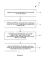
- Figure 6 illustrates schematically a method 10 of producing a textured silicon substrate according to an embodiment of this invention.
- a silicon substrate in the form of a silicon wafer is provided at step 12.
- the silicon substrate has a surface layer of silica.
- Silica films may be formed on the surface of silicon wafers in a number of different ways, for example either by coating with silica or by exposure to air either at ambient or elevated temperature.
- the "as received" silicon wafers have a thin layer of silica on the surface.
- the oxide of interest may be also formed in solutions, such as in polishing slurries.
- an electrical conductor is positioned in contact with the surface layer of silica to provide a silica/electrical conductor connection or interface.
- an electrochemical cell including a molten salt electrolyte is provided, with the silica/electrical conductor interface forming at least part of one electrode.
- the silicon wafers are made the cathode in a bath of calcium chloride.
- a cathodic potential is applied at step 18, without depositing a cation from the molten salt electrolyte.
- the wafers were washed and the surface characterized by examination in a scanning electron microscope, x-ray diffraction, x-ray photoelectron spectroscopy and the measurement of reflectance.
- Analytical grade anhydrous CaCl 2 was used to prepare the electrolyte.
- the salt was kept under vacuum at elevated temperatures to remove residual water and Ca(OH) 2 .
- the heating pattern involved an increase of temperature from ambient to 80°C and holding for 3 hours, then to 120°C, holding for 3 hours, and finally to 180°C, holding for 18 hours.
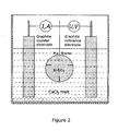
- a cylindrical alumina crucible was used to house the electrochemical cell whose height was 100 mm and wall thickness was 3 mm.
- the crucible was filled with salt and placed inside a stainless steel reactor in a vertical tube furnace (Instron SFL, UK).
- the salt was melted at 850°C.
- the depth of electrolyte in the crucible was about 4cm.
- P-type silicon wafers sliced from a ⁇ 100>single-crystal were used (from Si-Mat GmbH, Germany). Diameter of the wafer was about 5 cm (about 2"), geometric area
- Graphite cylindrical rods served both as pseudo-reference and counter electrodes.
- the graphite electrode was calibrated by measuring the potential for calcium deposition. This was at ca. -1.5 V and exhibited god reproducibility.
- the initial three-phase interface is composed from the electronic conductor (Mo), the oxide (SiO 2 ) and the electrolyte (CaCl 2 ).
- Mo electronic conductor
- SiO 2 oxide
- CaCl 2 electrolyte
- the electrochemical silicon reduction starts at the interface Mo-SiO 2 -CaCl 2 SiO 2 +4e - ⁇ Si + 2O 2- (1)
- the oxygen ions are removed by diffusion to electrolyte and the produced silicon takes a further role of an electronic conductor by forming a new three-phase interface Si-SiO2-CaCl 2 .
- the reduced silicon Once the reduced silicon has contact with the silicon substrate, the entire wafer starts to act as an electronic conductor.
- Fig. 3b shows on a micrometer scale the surface features of the silica precursor deoxygenated for 3 min. The process has spread over the surface, however, some micrometer-sized locations remain still poorly covered (the dark zone in the Figure). The filament-like formations in such locations imply traces of three-phase interface lines. The surface shows great ability to absorb visible light.
- Fig. 3c,d shows surface features at nano-micro scale after 17 minutes of electrolysis. Globular structures including single nano-spheroids are formed, which tend to agglomerate and confine void spaces, i.e. pores ( Fig. 3c ). The pore size is of the order of hundreds of nanometers, thus, they could be ascribed to macropores.
- the micropores are those below 2 nm in diameter, the mesopores in the range 2 nm to 50 nm and the macropores greater than 50 nm.
- a fine nanofibre structure decorates the porous layer, which is well identified on the side-view of the cleaved sample ( Fig. 3d ). The side-view identifies also the surface layer shrinking due to the oxygen leaving the silica layer.
- thickness of the deoxidated structure is less than 1 ⁇ m.
- the depth of the pores is of the order of hundreds of nanometers.
- the fibre structure is composed of the filaments, whose thickness is of the order of tens of nanometers.
- the deoxygenated layer exhibits specifically high surface to volume ratio providing a large surface area for light trapping.
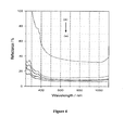
- the surface showed the reflectivity around 8 % in a wide visible region ( Fig. 4 ).
- Extension of the electrolysis time to 1 h did not improve the antireflection properties ( ⁇ 11 %, Fig. 4 ). It may be, therefore, concluded that the initial structures of the deoxygenated surface are most effective in terms of light trapping performance.
- the next example shows black silicon formation using silicon wafer with a very thin silica layer (10 nm) as a precursor. Nano-roughness was achieved by deoxygenating of such layer. The surface features are shown in Fig. 5 . The surface is composed of nano-crystals whose size is less then 100 nm. The sample absorbs effectively visible light - ca. 6% reflectance was found within a wide wavelength region.
Landscapes
- Chemical & Material Sciences (AREA)
- Chemical Kinetics & Catalysis (AREA)
- Electrochemistry (AREA)
- Engineering & Computer Science (AREA)
- Organic Chemistry (AREA)
- Metallurgy (AREA)
- Materials Engineering (AREA)
- Inorganic Chemistry (AREA)
- General Chemical & Material Sciences (AREA)
- Silicon Compounds (AREA)
- Electrolytic Production Of Non-Metals, Compounds, Apparatuses Therefor (AREA)
- Photovoltaic Devices (AREA)
- Manufacturing & Machinery (AREA)
Claims (15)
- Procédé de production d'une surface en silicium texturée, comprenant les opérations consistant à :doter un substrat en silicium d'une couche superficielle de silice ;attacher un conducteur électrique à la couche superficielle de silice afin de procurer une connexion silice / conducteur électrique ;mettre à disposition une cellule électrolytique incluant un électrolyte à sels fondus, alors que la connexion silice / conducteur électrique constitue au moins une partie d'une électrode ;appliquer un potentiel au conducteur électrique lequel est suffisant pour réduire la couche superficielle de silice sans déposer un cation provenant de l'électrolyte à sels fondus.
- Procédé selon la revendication 1, comprenant en outre l'opération consistant à :former la couche superficielle de silice grâce à l'enduction du substrat de silicium avec de la silice.
- Procédé selon la revendication 1, comprenant en outre l'opération consistant à :former la couche superficielle de silice grâce à l'oxydation du substrat de silicium.
- Procédé selon l'une quelconque des revendications précédentes, dans lequel le conducteur électrique est stable dans l'électrolyte à sels fondus.
- Procédé selon la revendication 4, le conducteur électrique étant sélectionné à partir du groupe composé de molybdène et de tungstène.
- Procédé selon l'une quelconque des revendications précédentes, dans lequel l'électrolyte à sels fondus est à une température allant de 500°C à 1000°C.
- Procédé selon l'une quelconque des revendications précédentes, dans lequel l'électrolyte à sels fondus comprend ou est composé d'un halogénure de calcium, baryum, strontium ou lithium.
- Procédé selon la revendication 7, dans lequel l'électrolyte à sels fondus est du chlorure de calcium.
- Procédé selon l'une quelconque des revendications 1 à 5, dans lequel l'électrolyte à sels fondus a un point de fusion inférieur à 100°C.
- Procédé selon l'une quelconque des revendications précédentes, dans lequel un dépôt de cations provenant de l'électrolyte à sels fondus est évité grâce à la détermination d'un potentiel de dépôt pour commencer le dépôt de cations dans la cellule électrolytique, et en veillant à ce que le potentiel appliqué ne dépasse pas le potentiel de dépôt.
- Procédé selon l'une quelconque des revendications précédentes, comprenant en outre l'opération consistant à maintenir le potentiel appliqué jusqu'à ce que la couche superficielle de silice développe une morphologie superficielle avec la formation de structures globulaires incluant des nano-sphéroïdes individuels.
- Procédé selon la revendication 11, dans lequel la morphologie superficielle inclut des pores, chacun ayant un diamètre d'au moins 50 nm.
- Procédé selon l'une quelconque des revendications précédentes, dans lequel la cellule électrolytique a une anode laquelle est formée à l'aide d'une matière inerte.
- Procédé selon la revendication 11 ou la revendication 12, dans lequel la morphologie superficielle a une microstructure qui est plus fine que 1 micron.
- Procédé selon la revendication 11, dans lequel la morphologie superficielle a une microstructure qui est plus fine que 100 nm.
Applications Claiming Priority (2)
| Application Number | Priority Date | Filing Date | Title |
|---|---|---|---|
| GBGB1010772.0A GB201010772D0 (en) | 2010-06-26 | 2010-06-26 | Method for texturing silicon surfaces |
| PCT/GB2011/051213 WO2011161479A1 (fr) | 2010-06-26 | 2011-06-27 | Procédé de texturation d'une surface en silicium pour créer un silicium noir pour des applications photovoltaïques |
Publications (2)
| Publication Number | Publication Date |
|---|---|
| EP2586064A1 EP2586064A1 (fr) | 2013-05-01 |
| EP2586064B1 true EP2586064B1 (fr) | 2015-06-17 |
Family
ID=42583042
Family Applications (1)
| Application Number | Title | Priority Date | Filing Date |
|---|---|---|---|
| EP11754717.4A Not-in-force EP2586064B1 (fr) | 2010-06-26 | 2011-06-27 | Procede de texturation d'une surface en silicium pour creer un silicium noir pour des applications photovoltaïques |
Country Status (6)
| Country | Link |
|---|---|
| US (1) | US8790953B2 (fr) |
| EP (1) | EP2586064B1 (fr) |
| JP (1) | JP5689530B2 (fr) |
| CN (1) | CN102971858B (fr) |
| GB (2) | GB201010772D0 (fr) |
| WO (1) | WO2011161479A1 (fr) |
Cited By (1)
| Publication number | Priority date | Publication date | Assignee | Title |
|---|---|---|---|---|
| US10276740B1 (en) | 2018-03-19 | 2019-04-30 | The United States Of America As Represented By The Secretary Of The Air Force | Co-deposition of black silicon |
Families Citing this family (13)
| Publication number | Priority date | Publication date | Assignee | Title |
|---|---|---|---|---|
| US8815104B2 (en) | 2008-03-21 | 2014-08-26 | Alliance For Sustainable Energy, Llc | Copper-assisted, anti-reflection etching of silicon surfaces |
| US8729798B2 (en) | 2008-03-21 | 2014-05-20 | Alliance For Sustainable Energy, Llc | Anti-reflective nanoporous silicon for efficient hydrogen production |
| US9034216B2 (en) | 2009-11-11 | 2015-05-19 | Alliance For Sustainable Energy, Llc | Wet-chemical systems and methods for producing black silicon substrates |
| US8828765B2 (en) | 2010-06-09 | 2014-09-09 | Alliance For Sustainable Energy, Llc | Forming high efficiency silicon solar cells using density-graded anti-reflection surfaces |
| CN110289320A (zh) * | 2011-03-08 | 2019-09-27 | 可持续能源联盟有限责任公司 | 蓝光响应增强的高效黑硅光伏器件 |
| CN103367476B (zh) * | 2012-03-27 | 2015-12-16 | 电子科技大学 | 一种n+/n型黑硅新结构及制备工艺 |
| CN102738309A (zh) * | 2012-07-11 | 2012-10-17 | 辽宁朝阳太阳能科技有限公司 | 双面高效陷光纳米绒面的双pn结晶硅太阳能电池制造方法 |
| DE102014111781B4 (de) | 2013-08-19 | 2022-08-11 | Korea Atomic Energy Research Institute | Verfahren zur elektrochemischen Herstellung einer Silizium-Schicht |
| KR101642026B1 (ko) * | 2013-08-19 | 2016-07-22 | 한국원자력연구원 | 전기화학적 실리콘 막 제조방법 |
| CN105047764A (zh) * | 2015-09-01 | 2015-11-11 | 浙江晶科能源有限公司 | 一种硅片的制绒方法 |
| US11164733B2 (en) | 2015-10-07 | 2021-11-02 | The Regents Of The University Of California | Fabrication of mass spectrometry surface |
| GB201704586D0 (en) * | 2017-03-23 | 2017-05-10 | Blacksilicon Ltd | Electrodes for metal- ion batteries |
| US20240372061A1 (en) * | 2023-05-04 | 2024-11-07 | Ford Global Technologies, Llc | Expanded bulk silicon anode material |
Family Cites Families (5)
| Publication number | Priority date | Publication date | Assignee | Title |
|---|---|---|---|---|
| JP2000261008A (ja) * | 1999-03-10 | 2000-09-22 | Mitsubishi Electric Corp | 太陽電池用シリコン基板の粗面化方法 |
| MXPA04008887A (es) * | 2002-03-13 | 2004-11-26 | Bhp Billiton Innovation Pty | Reduccion de oxidos de metal en una celda electrolitica. |
| JP4765066B2 (ja) * | 2005-05-19 | 2011-09-07 | 国立大学法人京都大学 | シリコンの製造方法 |
| NL1031734C2 (nl) * | 2006-05-03 | 2007-11-06 | Girasolar B V | Werkwijze voor het zuiveren van een halfgeleidermateriaal onder toepassing van een oxidatie-reductiereactie. |
| US20090236317A1 (en) * | 2008-03-21 | 2009-09-24 | Midwest Research Institute | Anti-reflection etching of silicon surfaces catalyzed with ionic metal solutions |
-
2010
- 2010-06-26 GB GBGB1010772.0A patent/GB201010772D0/en not_active Ceased
-
2011
- 2011-06-27 US US13/805,247 patent/US8790953B2/en not_active Expired - Fee Related
- 2011-06-27 GB GB1221891.3A patent/GB2494566B/en not_active Expired - Fee Related
- 2011-06-27 JP JP2013515974A patent/JP5689530B2/ja not_active Expired - Fee Related
- 2011-06-27 CN CN201180030064.0A patent/CN102971858B/zh not_active Expired - Fee Related
- 2011-06-27 EP EP11754717.4A patent/EP2586064B1/fr not_active Not-in-force
- 2011-06-27 WO PCT/GB2011/051213 patent/WO2011161479A1/fr not_active Ceased
Cited By (1)
| Publication number | Priority date | Publication date | Assignee | Title |
|---|---|---|---|---|
| US10276740B1 (en) | 2018-03-19 | 2019-04-30 | The United States Of America As Represented By The Secretary Of The Air Force | Co-deposition of black silicon |
Also Published As
| Publication number | Publication date |
|---|---|
| US20130095596A1 (en) | 2013-04-18 |
| GB2494566A (en) | 2013-03-13 |
| GB2494566B (en) | 2014-05-28 |
| US8790953B2 (en) | 2014-07-29 |
| CN102971858B (zh) | 2015-04-22 |
| JP2013532385A (ja) | 2013-08-15 |
| WO2011161479A1 (fr) | 2011-12-29 |
| CN102971858A (zh) | 2013-03-13 |
| EP2586064A1 (fr) | 2013-05-01 |
| JP5689530B2 (ja) | 2015-03-25 |
| GB201010772D0 (en) | 2010-08-11 |
Similar Documents
| Publication | Publication Date | Title |
|---|---|---|
| US8790953B2 (en) | Method for texturing silicon surface to create black silicon for photovoltaic applications | |
| Dubale et al. | Heterostructured Cu 2 O/CuO decorated with nickel as a highly efficient photocathode for photoelectrochemical water reduction | |
| Chernomordik et al. | Photoelectrochemical activity of as-grown, α-Fe2O3 nanowire array electrodes for water splitting | |
| Wang et al. | Au nanoparticle sensitized ZnO nanopencil arrays for photoelectrochemical water splitting | |
| Wu et al. | Enhanced supercapacitance in anodic TiO2 nanotube films by hydrogen plasma treatment | |
| Srivastava et al. | Large area fabrication of vertical silicon nanowire arrays by silver-assisted single-step chemical etching and their formation kinetics | |
| De Jongh et al. | Cu2O: electrodeposition and characterization | |
| Ruan et al. | Fabrication of highly ordered TiO2 nanotube arrays using an organic electrolyte | |
| US10738387B2 (en) | Electrochemical cell containing a graphene coated electrode | |
| Fan et al. | Stable and efficient multi-crystalline n+ p silicon photocathode for H2 production with pyramid-like surface nanostructure and thin Al2O3 protective layer | |
| Yang et al. | Fabrication and catalytic properties of Co− Ag− Pt nanoparticle-decorated titania nanotube arrays | |
| JPS60163365A (ja) | 無定形炭素電極からなる電池およびその電極で電気化学反応を行う方法 | |
| Lai et al. | Preparation of tin dioxide nanotubes via electrosynthesis in a template | |
| Naseri et al. | Applying alloyed metal nanoparticles to enhance solar assisted water splitting | |
| TW201330294A (zh) | 奈米結構區域的電性接點 | |
| Juzeliunas et al. | Silicon surface texturing by electro-deoxidation of a thin silica layer in molten salt | |
| Yang et al. | Enhanced photoelectrochemical performance and charge transfer properties in self-organized NiOx-doped TiO2 nanotubes | |
| Juzeliunas et al. | Electro-deoxidation of thin silica layer in molten salt—Globular structures with effective light absorbance | |
| Djenizian et al. | Electrochemical fabrication of Sn nanowires on titania nanotube guide layers | |
| Ishihara et al. | A novel tungsten trioxide (WO 3)/ITO porous nanocomposite for enhanced photo-catalytic water splitting | |
| Isimjan et al. | The fabrication of highly ordered and visible-light-responsive Fe–C–N-codoped TiO2 nanotubes | |
| Dev et al. | A plausible impact on the role of pulses in anodized TiO2 nanotube arrays enhancing Ti3+ defects | |
| Tang et al. | The formation of micrometer-long TiO2 nanotube arrays by anodization of titanium film on conducting glass substrate | |
| Kolay et al. | Graphene nanoparticles-decorated silicon nanowires with tungsten oxide counter electrode for quasi-solid state hybrid solar cells | |
| Lai | Surface morphology and growth of anodic titania nanotubes films: photoelectrochemical water splitting studies |
Legal Events
| Date | Code | Title | Description |
|---|---|---|---|
| PUAI | Public reference made under article 153(3) epc to a published international application that has entered the european phase |
Free format text: ORIGINAL CODE: 0009012 |
|
| 17P | Request for examination filed |
Effective date: 20130108 |
|
| AK | Designated contracting states |
Kind code of ref document: A1 Designated state(s): AL AT BE BG CH CY CZ DE DK EE ES FI FR GB GR HR HU IE IS IT LI LT LU LV MC MK MT NL NO PL PT RO RS SE SI SK SM TR |
|
| DAX | Request for extension of the european patent (deleted) | ||
| RIC1 | Information provided on ipc code assigned before grant |
Ipc: H01L 31/0236 20060101AFI20150113BHEP Ipc: C25B 1/00 20060101ALI20150113BHEP |
|
| GRAP | Despatch of communication of intention to grant a patent |
Free format text: ORIGINAL CODE: EPIDOSNIGR1 |
|
| INTG | Intention to grant announced |
Effective date: 20150305 |
|
| GRAS | Grant fee paid |
Free format text: ORIGINAL CODE: EPIDOSNIGR3 |
|
| GRAA | (expected) grant |
Free format text: ORIGINAL CODE: 0009210 |
|
| AK | Designated contracting states |
Kind code of ref document: B1 Designated state(s): AL AT BE BG CH CY CZ DE DK EE ES FI FR GB GR HR HU IE IS IT LI LT LU LV MC MK MT NL NO PL PT RO RS SE SI SK SM TR |
|
| REG | Reference to a national code |
Ref country code: GB Ref legal event code: FG4D |
|
| REG | Reference to a national code |
Ref country code: CH Ref legal event code: EP |
|
| REG | Reference to a national code |
Ref country code: AT Ref legal event code: REF Ref document number: 732344 Country of ref document: AT Kind code of ref document: T Effective date: 20150715 |
|
| REG | Reference to a national code |
Ref country code: IE Ref legal event code: FG4D |
|
| REG | Reference to a national code |
Ref country code: DE Ref legal event code: R096 Ref document number: 602011017219 Country of ref document: DE |
|
| REG | Reference to a national code |
Ref country code: NO Ref legal event code: T2 Effective date: 20150617 |
|
| PG25 | Lapsed in a contracting state [announced via postgrant information from national office to epo] |
Ref country code: LT Free format text: LAPSE BECAUSE OF FAILURE TO SUBMIT A TRANSLATION OF THE DESCRIPTION OR TO PAY THE FEE WITHIN THE PRESCRIBED TIME-LIMIT Effective date: 20150617 Ref country code: HR Free format text: LAPSE BECAUSE OF FAILURE TO SUBMIT A TRANSLATION OF THE DESCRIPTION OR TO PAY THE FEE WITHIN THE PRESCRIBED TIME-LIMIT Effective date: 20150617 Ref country code: FI Free format text: LAPSE BECAUSE OF FAILURE TO SUBMIT A TRANSLATION OF THE DESCRIPTION OR TO PAY THE FEE WITHIN THE PRESCRIBED TIME-LIMIT Effective date: 20150617 |
|
| REG | Reference to a national code |
Ref country code: AT Ref legal event code: MK05 Ref document number: 732344 Country of ref document: AT Kind code of ref document: T Effective date: 20150617 |
|
| REG | Reference to a national code |
Ref country code: LT Ref legal event code: MG4D Ref country code: NL Ref legal event code: MP Effective date: 20150617 |
|
| PG25 | Lapsed in a contracting state [announced via postgrant information from national office to epo] |
Ref country code: BG Free format text: LAPSE BECAUSE OF FAILURE TO SUBMIT A TRANSLATION OF THE DESCRIPTION OR TO PAY THE FEE WITHIN THE PRESCRIBED TIME-LIMIT Effective date: 20150917 Ref country code: RS Free format text: LAPSE BECAUSE OF FAILURE TO SUBMIT A TRANSLATION OF THE DESCRIPTION OR TO PAY THE FEE WITHIN THE PRESCRIBED TIME-LIMIT Effective date: 20150617 Ref country code: LV Free format text: LAPSE BECAUSE OF FAILURE TO SUBMIT A TRANSLATION OF THE DESCRIPTION OR TO PAY THE FEE WITHIN THE PRESCRIBED TIME-LIMIT Effective date: 20150617 Ref country code: GR Free format text: LAPSE BECAUSE OF FAILURE TO SUBMIT A TRANSLATION OF THE DESCRIPTION OR TO PAY THE FEE WITHIN THE PRESCRIBED TIME-LIMIT Effective date: 20150918 |
|
| PG25 | Lapsed in a contracting state [announced via postgrant information from national office to epo] |
Ref country code: IT Free format text: LAPSE BECAUSE OF FAILURE TO SUBMIT A TRANSLATION OF THE DESCRIPTION OR TO PAY THE FEE WITHIN THE PRESCRIBED TIME-LIMIT Effective date: 20150617 Ref country code: EE Free format text: LAPSE BECAUSE OF FAILURE TO SUBMIT A TRANSLATION OF THE DESCRIPTION OR TO PAY THE FEE WITHIN THE PRESCRIBED TIME-LIMIT Effective date: 20150617 |
|
| REG | Reference to a national code |
Ref country code: CH Ref legal event code: PL |
|
| PG25 | Lapsed in a contracting state [announced via postgrant information from national office to epo] |
Ref country code: SK Free format text: LAPSE BECAUSE OF FAILURE TO SUBMIT A TRANSLATION OF THE DESCRIPTION OR TO PAY THE FEE WITHIN THE PRESCRIBED TIME-LIMIT Effective date: 20150617 Ref country code: CZ Free format text: LAPSE BECAUSE OF FAILURE TO SUBMIT A TRANSLATION OF THE DESCRIPTION OR TO PAY THE FEE WITHIN THE PRESCRIBED TIME-LIMIT Effective date: 20150617 Ref country code: PL Free format text: LAPSE BECAUSE OF FAILURE TO SUBMIT A TRANSLATION OF THE DESCRIPTION OR TO PAY THE FEE WITHIN THE PRESCRIBED TIME-LIMIT Effective date: 20150617 Ref country code: IS Free format text: LAPSE BECAUSE OF FAILURE TO SUBMIT A TRANSLATION OF THE DESCRIPTION OR TO PAY THE FEE WITHIN THE PRESCRIBED TIME-LIMIT Effective date: 20151017 Ref country code: RO Free format text: LAPSE BECAUSE OF NON-PAYMENT OF DUE FEES Effective date: 20150617 Ref country code: AT Free format text: LAPSE BECAUSE OF FAILURE TO SUBMIT A TRANSLATION OF THE DESCRIPTION OR TO PAY THE FEE WITHIN THE PRESCRIBED TIME-LIMIT Effective date: 20150617 Ref country code: PT Free format text: LAPSE BECAUSE OF FAILURE TO SUBMIT A TRANSLATION OF THE DESCRIPTION OR TO PAY THE FEE WITHIN THE PRESCRIBED TIME-LIMIT Effective date: 20151019 Ref country code: ES Free format text: LAPSE BECAUSE OF FAILURE TO SUBMIT A TRANSLATION OF THE DESCRIPTION OR TO PAY THE FEE WITHIN THE PRESCRIBED TIME-LIMIT Effective date: 20150617 |
|
| REG | Reference to a national code |
Ref country code: DE Ref legal event code: R097 Ref document number: 602011017219 Country of ref document: DE |
|
| REG | Reference to a national code |
Ref country code: IE Ref legal event code: MM4A |
|
| PG25 | Lapsed in a contracting state [announced via postgrant information from national office to epo] |
Ref country code: MC Free format text: LAPSE BECAUSE OF FAILURE TO SUBMIT A TRANSLATION OF THE DESCRIPTION OR TO PAY THE FEE WITHIN THE PRESCRIBED TIME-LIMIT Effective date: 20150617 |
|
| PLBE | No opposition filed within time limit |
Free format text: ORIGINAL CODE: 0009261 |
|
| STAA | Information on the status of an ep patent application or granted ep patent |
Free format text: STATUS: NO OPPOSITION FILED WITHIN TIME LIMIT |
|
| PG25 | Lapsed in a contracting state [announced via postgrant information from national office to epo] |
Ref country code: IE Free format text: LAPSE BECAUSE OF NON-PAYMENT OF DUE FEES Effective date: 20150627 Ref country code: CH Free format text: LAPSE BECAUSE OF NON-PAYMENT OF DUE FEES Effective date: 20150630 Ref country code: DK Free format text: LAPSE BECAUSE OF FAILURE TO SUBMIT A TRANSLATION OF THE DESCRIPTION OR TO PAY THE FEE WITHIN THE PRESCRIBED TIME-LIMIT Effective date: 20150617 Ref country code: LI Free format text: LAPSE BECAUSE OF NON-PAYMENT OF DUE FEES Effective date: 20150630 |
|
| 26N | No opposition filed |
Effective date: 20160318 |
|
| REG | Reference to a national code |
Ref country code: FR Ref legal event code: PLFP Year of fee payment: 6 |
|
| PG25 | Lapsed in a contracting state [announced via postgrant information from national office to epo] |
Ref country code: SI Free format text: LAPSE BECAUSE OF FAILURE TO SUBMIT A TRANSLATION OF THE DESCRIPTION OR TO PAY THE FEE WITHIN THE PRESCRIBED TIME-LIMIT Effective date: 20150617 |
|
| PG25 | Lapsed in a contracting state [announced via postgrant information from national office to epo] |
Ref country code: MT Free format text: LAPSE BECAUSE OF FAILURE TO SUBMIT A TRANSLATION OF THE DESCRIPTION OR TO PAY THE FEE WITHIN THE PRESCRIBED TIME-LIMIT Effective date: 20150617 Ref country code: BE Free format text: LAPSE BECAUSE OF FAILURE TO SUBMIT A TRANSLATION OF THE DESCRIPTION OR TO PAY THE FEE WITHIN THE PRESCRIBED TIME-LIMIT Effective date: 20150617 |
|
| PG25 | Lapsed in a contracting state [announced via postgrant information from national office to epo] |
Ref country code: HU Free format text: LAPSE BECAUSE OF FAILURE TO SUBMIT A TRANSLATION OF THE DESCRIPTION OR TO PAY THE FEE WITHIN THE PRESCRIBED TIME-LIMIT; INVALID AB INITIO Effective date: 20110627 Ref country code: SM Free format text: LAPSE BECAUSE OF FAILURE TO SUBMIT A TRANSLATION OF THE DESCRIPTION OR TO PAY THE FEE WITHIN THE PRESCRIBED TIME-LIMIT Effective date: 20150617 |
|
| REG | Reference to a national code |
Ref country code: FR Ref legal event code: PLFP Year of fee payment: 7 |
|
| PG25 | Lapsed in a contracting state [announced via postgrant information from national office to epo] |
Ref country code: NL Free format text: LAPSE BECAUSE OF FAILURE TO SUBMIT A TRANSLATION OF THE DESCRIPTION OR TO PAY THE FEE WITHIN THE PRESCRIBED TIME-LIMIT Effective date: 20150617 Ref country code: CY Free format text: LAPSE BECAUSE OF FAILURE TO SUBMIT A TRANSLATION OF THE DESCRIPTION OR TO PAY THE FEE WITHIN THE PRESCRIBED TIME-LIMIT Effective date: 20150617 Ref country code: SE Free format text: LAPSE BECAUSE OF FAILURE TO SUBMIT A TRANSLATION OF THE DESCRIPTION OR TO PAY THE FEE WITHIN THE PRESCRIBED TIME-LIMIT Effective date: 20150617 |
|
| PG25 | Lapsed in a contracting state [announced via postgrant information from national office to epo] |
Ref country code: TR Free format text: LAPSE BECAUSE OF FAILURE TO SUBMIT A TRANSLATION OF THE DESCRIPTION OR TO PAY THE FEE WITHIN THE PRESCRIBED TIME-LIMIT Effective date: 20150617 |
|
| PG25 | Lapsed in a contracting state [announced via postgrant information from national office to epo] |
Ref country code: LU Free format text: LAPSE BECAUSE OF NON-PAYMENT OF DUE FEES Effective date: 20150627 |
|
| REG | Reference to a national code |
Ref country code: FR Ref legal event code: PLFP Year of fee payment: 8 |
|
| PG25 | Lapsed in a contracting state [announced via postgrant information from national office to epo] |
Ref country code: MK Free format text: LAPSE BECAUSE OF FAILURE TO SUBMIT A TRANSLATION OF THE DESCRIPTION OR TO PAY THE FEE WITHIN THE PRESCRIBED TIME-LIMIT Effective date: 20150617 |
|
| PG25 | Lapsed in a contracting state [announced via postgrant information from national office to epo] |
Ref country code: AL Free format text: LAPSE BECAUSE OF FAILURE TO SUBMIT A TRANSLATION OF THE DESCRIPTION OR TO PAY THE FEE WITHIN THE PRESCRIBED TIME-LIMIT Effective date: 20150617 |
|
| PGFP | Annual fee paid to national office [announced via postgrant information from national office to epo] |
Ref country code: DE Payment date: 20190609 Year of fee payment: 9 Ref country code: NO Payment date: 20190618 Year of fee payment: 9 |
|
| PGFP | Annual fee paid to national office [announced via postgrant information from national office to epo] |
Ref country code: FR Payment date: 20190605 Year of fee payment: 9 |
|
| PGFP | Annual fee paid to national office [announced via postgrant information from national office to epo] |
Ref country code: GB Payment date: 20190604 Year of fee payment: 9 |
|
| REG | Reference to a national code |
Ref country code: NO Ref legal event code: CHAD Owner name: BLACKSILICON LIMITED, KY |
|
| REG | Reference to a national code |
Ref country code: DE Ref legal event code: R082 Ref document number: 602011017219 Country of ref document: DE Representative=s name: RGTH RICHTER GERBAULET THIELEMANN HOFMANN PATE, DE Ref country code: DE Ref legal event code: R081 Ref document number: 602011017219 Country of ref document: DE Owner name: BLACKSILICON LIMITED, CAMANA BAY, KY Free format text: FORMER OWNERS: FRAY, DEREK JOHN, CAMBRIDGE, CAMBRIDGESHIRE, GB; JUZELIUNAS, EIMUTIS, CAMBRIDGE, GB |
|
| REG | Reference to a national code |
Ref country code: GB Ref legal event code: 732E Free format text: REGISTERED BETWEEN 20200220 AND 20200226 |
|
| REG | Reference to a national code |
Ref country code: DE Ref legal event code: R119 Ref document number: 602011017219 Country of ref document: DE |
|
| REG | Reference to a national code |
Ref country code: NO Ref legal event code: MMEP |
|
| GBPC | Gb: european patent ceased through non-payment of renewal fee |
Effective date: 20200627 |
|
| PG25 | Lapsed in a contracting state [announced via postgrant information from national office to epo] |
Ref country code: FR Free format text: LAPSE BECAUSE OF NON-PAYMENT OF DUE FEES Effective date: 20200630 Ref country code: GB Free format text: LAPSE BECAUSE OF NON-PAYMENT OF DUE FEES Effective date: 20200627 Ref country code: NO Free format text: LAPSE BECAUSE OF NON-PAYMENT OF DUE FEES Effective date: 20200630 |
|
| PG25 | Lapsed in a contracting state [announced via postgrant information from national office to epo] |
Ref country code: DE Free format text: LAPSE BECAUSE OF NON-PAYMENT OF DUE FEES Effective date: 20210101 |