EP2587546A2 - Solarzelle und Solarzellenmodul - Google Patents
Solarzelle und Solarzellenmodul Download PDFInfo
- Publication number
- EP2587546A2 EP2587546A2 EP12181729.0A EP12181729A EP2587546A2 EP 2587546 A2 EP2587546 A2 EP 2587546A2 EP 12181729 A EP12181729 A EP 12181729A EP 2587546 A2 EP2587546 A2 EP 2587546A2
- Authority
- EP
- European Patent Office
- Prior art keywords
- finger electrodes
- bus bar
- solar cell
- conducting section
- conducting
- Prior art date
- Legal status (The legal status is an assumption and is not a legal conclusion. Google has not performed a legal analysis and makes no representation as to the accuracy of the status listed.)
- Withdrawn
Links
- 238000006243 chemical reaction Methods 0.000 claims abstract description 25
- 238000007650 screen-printing Methods 0.000 claims description 28
- 238000000034 method Methods 0.000 description 11
- 239000000758 substrate Substances 0.000 description 6
- 238000007639 printing Methods 0.000 description 5
- 239000004065 semiconductor Substances 0.000 description 5
- 238000004519 manufacturing process Methods 0.000 description 4
- 238000005476 soldering Methods 0.000 description 4
- 239000000853 adhesive Substances 0.000 description 3
- 230000001070 adhesive effect Effects 0.000 description 3
- 229910000679 solder Inorganic materials 0.000 description 3
- 239000000969 carrier Substances 0.000 description 2
- 239000004020 conductor Substances 0.000 description 2
- 238000010304 firing Methods 0.000 description 2
- 238000002161 passivation Methods 0.000 description 2
- 229910052581 Si3N4 Inorganic materials 0.000 description 1
- 229910004205 SiNX Inorganic materials 0.000 description 1
- XUIMIQQOPSSXEZ-UHFFFAOYSA-N Silicon Chemical compound [Si] XUIMIQQOPSSXEZ-UHFFFAOYSA-N 0.000 description 1
- 239000002313 adhesive film Substances 0.000 description 1
- 238000004873 anchoring Methods 0.000 description 1
- 230000015572 biosynthetic process Effects 0.000 description 1
- 239000013078 crystal Substances 0.000 description 1
- 229910021419 crystalline silicon Inorganic materials 0.000 description 1
- 230000002708 enhancing effect Effects 0.000 description 1
- 239000005038 ethylene vinyl acetate Substances 0.000 description 1
- 239000000463 material Substances 0.000 description 1
- 238000002844 melting Methods 0.000 description 1
- 230000008018 melting Effects 0.000 description 1
- 230000004048 modification Effects 0.000 description 1
- 238000012986 modification Methods 0.000 description 1
- 238000012858 packaging process Methods 0.000 description 1
- 238000005215 recombination Methods 0.000 description 1
- 230000006798 recombination Effects 0.000 description 1
- 229910052710 silicon Inorganic materials 0.000 description 1
- 239000010703 silicon Substances 0.000 description 1
- HQVNEWCFYHHQES-UHFFFAOYSA-N silicon nitride Chemical compound N12[Si]34N5[Si]62N3[Si]51N64 HQVNEWCFYHHQES-UHFFFAOYSA-N 0.000 description 1
Images


Classifications
-
- H—ELECTRICITY
- H10—SEMICONDUCTOR DEVICES; ELECTRIC SOLID-STATE DEVICES NOT OTHERWISE PROVIDED FOR
- H10F—INORGANIC SEMICONDUCTOR DEVICES SENSITIVE TO INFRARED RADIATION, LIGHT, ELECTROMAGNETIC RADIATION OF SHORTER WAVELENGTH OR CORPUSCULAR RADIATION
- H10F77/00—Constructional details of devices covered by this subclass
- H10F77/20—Electrodes
- H10F77/206—Electrodes for devices having potential barriers
- H10F77/211—Electrodes for devices having potential barriers for photovoltaic cells
- H10F77/215—Geometries of grid contacts
-
- H—ELECTRICITY
- H10—SEMICONDUCTOR DEVICES; ELECTRIC SOLID-STATE DEVICES NOT OTHERWISE PROVIDED FOR
- H10F—INORGANIC SEMICONDUCTOR DEVICES SENSITIVE TO INFRARED RADIATION, LIGHT, ELECTROMAGNETIC RADIATION OF SHORTER WAVELENGTH OR CORPUSCULAR RADIATION
- H10F19/00—Integrated devices, or assemblies of multiple devices, comprising at least one photovoltaic cell covered by group H10F10/00, e.g. photovoltaic modules
- H10F19/90—Structures for connecting between photovoltaic cells, e.g. interconnections or insulating spacers
- H10F19/902—Structures for connecting between photovoltaic cells, e.g. interconnections or insulating spacers for series or parallel connection of photovoltaic cells
-
- Y—GENERAL TAGGING OF NEW TECHNOLOGICAL DEVELOPMENTS; GENERAL TAGGING OF CROSS-SECTIONAL TECHNOLOGIES SPANNING OVER SEVERAL SECTIONS OF THE IPC; TECHNICAL SUBJECTS COVERED BY FORMER USPC CROSS-REFERENCE ART COLLECTIONS [XRACs] AND DIGESTS
- Y02—TECHNOLOGIES OR APPLICATIONS FOR MITIGATION OR ADAPTATION AGAINST CLIMATE CHANGE
- Y02E—REDUCTION OF GREENHOUSE GAS [GHG] EMISSIONS, RELATED TO ENERGY GENERATION, TRANSMISSION OR DISTRIBUTION
- Y02E10/00—Energy generation through renewable energy sources
- Y02E10/50—Photovoltaic [PV] energy
Definitions
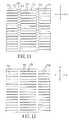
- a first conducive pattern 71 shown in Figure 11 is formed on the light-receiving surface 211 of the photoelectric conversion unit 21 (see Figure 10a ) using a screen (not shown) having a screen pattern corresponding to the first conductive pattern 71. Then, a process of baking is performed to dry the first conductive pattern 71.
Landscapes
- Photovoltaic Devices (AREA)
- Connection Of Batteries Or Terminals (AREA)
Applications Claiming Priority (1)
| Application Number | Priority Date | Filing Date | Title |
|---|---|---|---|
| TW100139125A TW201318187A (zh) | 2011-10-27 | 2011-10-27 | 太陽能電池及其模組 |
Publications (2)
| Publication Number | Publication Date |
|---|---|
| EP2587546A2 true EP2587546A2 (de) | 2013-05-01 |
| EP2587546A3 EP2587546A3 (de) | 2014-06-04 |
Family
ID=46796348
Family Applications (1)
| Application Number | Title | Priority Date | Filing Date |
|---|---|---|---|
| EP12181729.0A Withdrawn EP2587546A3 (de) | 2011-10-27 | 2012-08-24 | Solarzelle und Solarzellenmodul |
Country Status (5)
| Country | Link |
|---|---|
| US (1) | US20130104956A1 (de) |
| EP (1) | EP2587546A3 (de) |
| JP (1) | JP5469225B2 (de) |
| CN (1) | CN103094367B (de) |
| TW (1) | TW201318187A (de) |
Families Citing this family (11)
| Publication number | Priority date | Publication date | Assignee | Title |
|---|---|---|---|---|
| CN103236465B (zh) * | 2013-04-03 | 2016-03-02 | 苏州达方电子有限公司 | 元件上的电极结构及其制造方法 |
| TWI456782B (zh) * | 2013-06-05 | 2014-10-11 | Motech Ind Inc | 印刷用網版及應用該印刷用網版之太陽能電池的製造方法 |
| DE102013212845A1 (de) * | 2013-07-02 | 2015-01-08 | Solarworld Industries Sachsen Gmbh | Photovoltaikmodul |
| EP3582266B1 (de) * | 2014-09-30 | 2021-01-27 | Lg Electronics Inc. | Solarzelle und solarzellenplatte damit |
| US11532765B2 (en) * | 2015-04-30 | 2022-12-20 | Shangrao Jinko Solar Technology Development Co., Ltd | Solar cell and solar cell panel including the same |
| JP6628196B2 (ja) * | 2016-01-05 | 2020-01-08 | パナソニックIpマネジメント株式会社 | 太陽電池モジュール |
| JP2019204806A (ja) * | 2016-09-27 | 2019-11-28 | パナソニックIpマネジメント株式会社 | 太陽電池セル、太陽電池モジュール、及び太陽電池セルの製造方法 |
| JP6735894B2 (ja) * | 2017-02-16 | 2020-08-05 | 三菱電機株式会社 | 太陽電池セルの製造方法および太陽電池セル |
| CN109037363B (zh) * | 2018-07-24 | 2024-07-26 | 浙江爱旭太阳能科技有限公司 | 具有防断栅功能的晶硅太阳能电池的正电极 |
| TWI800190B (zh) * | 2021-12-30 | 2023-04-21 | 欣興電子股份有限公司 | 玻璃載板保護結構及其製法 |
| US20250374709A1 (en) * | 2024-06-03 | 2025-12-04 | Longi Green Energy Technology Co., Ltd. | Solar cell and photovoltaic module |
Family Cites Families (15)
| Publication number | Priority date | Publication date | Assignee | Title |
|---|---|---|---|---|
| JPS6138206Y2 (de) * | 1981-01-12 | 1986-11-05 | ||
| JP2703673B2 (ja) * | 1991-05-17 | 1998-01-26 | 三菱電機株式会社 | 半導体装置 |
| JP4255248B2 (ja) * | 2002-06-03 | 2009-04-15 | シャープ株式会社 | 太陽電池およびその製造方法 |
| US6936761B2 (en) * | 2003-03-29 | 2005-08-30 | Nanosolar, Inc. | Transparent electrode, optoelectronic apparatus and devices |
| JPWO2005109524A1 (ja) * | 2004-05-07 | 2008-03-21 | 三菱電機株式会社 | 太陽電池及びその製造方法 |
| JP5301758B2 (ja) * | 2005-05-19 | 2013-09-25 | 信越半導体株式会社 | 太陽電池 |
| JP2007103473A (ja) * | 2005-09-30 | 2007-04-19 | Sanyo Electric Co Ltd | 太陽電池装置および太陽電池モジュール |
| JP5203450B2 (ja) * | 2008-03-31 | 2013-06-05 | シャープ株式会社 | 太陽電池、太陽電池ストリングおよび太陽電池モジュール |
| JP2009272405A (ja) * | 2008-05-02 | 2009-11-19 | Mitsubishi Electric Corp | 太陽電池素子およびその製造方法 |
| JP5172480B2 (ja) * | 2008-06-04 | 2013-03-27 | シャープ株式会社 | 光電変換装置およびその製造方法 |
| TWM387372U (en) * | 2010-03-29 | 2010-08-21 | Neo Solar Power Corp | Electrode structure of solar cell |
| CN102152676A (zh) * | 2010-11-29 | 2011-08-17 | 奥特斯维能源(太仓)有限公司 | 一种节约式太阳能电池片栅线喷墨印刷工艺 |
| TWI434427B (zh) * | 2011-04-08 | 2014-04-11 | Gintech Energy Corp | 光伏面板及形成光伏面板之導電通道的方法 |
| US20120285519A1 (en) * | 2011-05-10 | 2012-11-15 | Emcore Solar Power, Inc. | Grid design for iii-v compound semiconductor cell |
| US9337363B2 (en) * | 2011-05-11 | 2016-05-10 | International Business Machines Corporation | Low resistance, low reflection, and low cost contact grids for photovoltaic cells |
-
2011
- 2011-10-27 TW TW100139125A patent/TW201318187A/zh not_active IP Right Cessation
-
2012
- 2012-01-06 CN CN201210003561.8A patent/CN103094367B/zh not_active Expired - Fee Related
- 2012-06-11 US US13/493,379 patent/US20130104956A1/en not_active Abandoned
- 2012-08-24 EP EP12181729.0A patent/EP2587546A3/de not_active Withdrawn
- 2012-10-17 JP JP2012229791A patent/JP5469225B2/ja not_active Expired - Fee Related
Non-Patent Citations (1)
| Title |
|---|
| None |
Also Published As
| Publication number | Publication date |
|---|---|
| TW201318187A (zh) | 2013-05-01 |
| US20130104956A1 (en) | 2013-05-02 |
| CN103094367B (zh) | 2015-06-24 |
| TWI496297B (de) | 2015-08-11 |
| EP2587546A3 (de) | 2014-06-04 |
| JP5469225B2 (ja) | 2014-04-16 |
| JP2013098548A (ja) | 2013-05-20 |
| CN103094367A (zh) | 2013-05-08 |
Similar Documents
| Publication | Publication Date | Title |
|---|---|---|
| EP2587546A2 (de) | Solarzelle und Solarzellenmodul | |
| JP4646558B2 (ja) | 太陽電池モジュール | |
| JP4738149B2 (ja) | 太陽電池モジュール | |
| EP2978025B1 (de) | Solarzelle und solarzellenmodul damit | |
| TWI603493B (zh) | 太陽能電池及其模組 | |
| KR20100019389A (ko) | 태양 전지 모듈 | |
| US20100193028A1 (en) | Solar cell | |
| EP2738816B1 (de) | Solarzelle, solarzellenmodul und verfahren zur herstellung einer solarzelle | |
| KR20110122176A (ko) | 태양전지 모듈 | |
| JP2011044750A (ja) | 太陽電池モジュール | |
| US9153713B2 (en) | Solar cell modules and methods of manufacturing the same | |
| US20180294367A1 (en) | Back contact solar cell substrate, method of manufacturing the same and back contact solar cell | |
| US20180219109A1 (en) | Solar module and method for manufacturing the solar module | |
| JP2010050350A (ja) | 太陽電池モジュール及び太陽電池 | |
| JP2015207598A (ja) | 太陽電池モジュール、太陽電池およびこれに用いられる素子間接続体 | |
| JP4953562B2 (ja) | 太陽電池モジュール | |
| US20190393369A1 (en) | Solar cell module | |
| JP5269014B2 (ja) | 太陽電池モジュール | |
| JP3198443U (ja) | 太陽電池モジュール | |
| CN104241404B (zh) | 太阳能电池及其模组 | |
| CN104218102A (zh) | 太阳能电池及其模组 | |
| JP2006210654A (ja) | 太陽電池素子及びこれを用いた太陽電池モジュール | |
| KR20190056550A (ko) | Mwt형 양면수광 태양전지 및 와이어 인터커넥터를 이용한 태양전지 모듈 | |
| KR20180000070A (ko) | 후면접합 양면수광형 태양전지 및 그 제조방법 | |
| KR20120081417A (ko) | 태양전지 및 그 제조방법 |
Legal Events
| Date | Code | Title | Description |
|---|---|---|---|
| PUAI | Public reference made under article 153(3) epc to a published international application that has entered the european phase |
Free format text: ORIGINAL CODE: 0009012 |
|
| 17P | Request for examination filed |
Effective date: 20120824 |
|
| AK | Designated contracting states |
Kind code of ref document: A2 Designated state(s): AL AT BE BG CH CY CZ DE DK EE ES FI FR GB GR HR HU IE IS IT LI LT LU LV MC MK MT NL NO PL PT RO RS SE SI SK SM TR |
|
| AX | Request for extension of the european patent |
Extension state: BA ME |
|
| RIC1 | Information provided on ipc code assigned before grant |
Ipc: H01L 31/0224 20060101AFI20140109BHEP Ipc: H01L 31/048 20060101ALI20140109BHEP Ipc: H01L 31/05 20060101ALI20140109BHEP |
|
| PUAL | Search report despatched |
Free format text: ORIGINAL CODE: 0009013 |
|
| AK | Designated contracting states |
Kind code of ref document: A3 Designated state(s): AL AT BE BG CH CY CZ DE DK EE ES FI FR GB GR HR HU IE IS IT LI LT LU LV MC MK MT NL NO PL PT RO RS SE SI SK SM TR |
|
| AX | Request for extension of the european patent |
Extension state: BA ME |
|
| RIC1 | Information provided on ipc code assigned before grant |
Ipc: H01L 31/048 20140101ALI20140425BHEP Ipc: H01L 31/05 20140101ALI20140425BHEP Ipc: H01L 31/0224 20060101AFI20140425BHEP |
|
| RBV | Designated contracting states (corrected) |
Designated state(s): AL AT BE BG CH CY CZ DE DK EE ES FI FR GB GR HR HU IE IS IT LI LT LU LV MC MK MT NL NO PL PT RO RS SE SI SK SM TR |
|
| 17Q | First examination report despatched |
Effective date: 20151111 |
|
| STAA | Information on the status of an ep patent application or granted ep patent |
Free format text: STATUS: THE APPLICATION IS DEEMED TO BE WITHDRAWN |
|
| 18D | Application deemed to be withdrawn |
Effective date: 20160322 |