EP2587554A2 - Verfahren zur Herstellung von Halbleiter-Lichtempfidlichensvorrichtungen - Google Patents
Verfahren zur Herstellung von Halbleiter-Lichtempfidlichensvorrichtungen Download PDFInfo
- Publication number
- EP2587554A2 EP2587554A2 EP12250166.1A EP12250166A EP2587554A2 EP 2587554 A2 EP2587554 A2 EP 2587554A2 EP 12250166 A EP12250166 A EP 12250166A EP 2587554 A2 EP2587554 A2 EP 2587554A2
- Authority
- EP
- European Patent Office
- Prior art keywords
- cap
- region
- wafer
- reflection coating
- front surface
- Prior art date
- Legal status (The legal status is an assumption and is not a legal conclusion. Google has not performed a legal analysis and makes no representation as to the accuracy of the status listed.)
- Withdrawn
Links
- 238000000034 method Methods 0.000 title claims abstract description 54
- 239000004065 semiconductor Substances 0.000 title claims abstract description 23
- 238000000576 coating method Methods 0.000 claims abstract description 31
- 239000011248 coating agent Substances 0.000 claims abstract description 30
- 238000001514 detection method Methods 0.000 claims abstract description 15
- 229910052751 metal Inorganic materials 0.000 claims description 47
- 239000002184 metal Substances 0.000 claims description 47
- 238000000059 patterning Methods 0.000 claims description 14
- 229920002120 photoresistant polymer Polymers 0.000 claims description 14
- 239000000758 substrate Substances 0.000 claims description 7
- 238000005530 etching Methods 0.000 claims description 5
- 238000000206 photolithography Methods 0.000 claims description 5
- 238000001459 lithography Methods 0.000 abstract description 10
- 238000004519 manufacturing process Methods 0.000 abstract description 8
- 238000000151 deposition Methods 0.000 description 7
- 238000001465 metallisation Methods 0.000 description 7
- 239000000969 carrier Substances 0.000 description 6
- 230000008021 deposition Effects 0.000 description 6
- 238000010586 diagram Methods 0.000 description 5
- 238000000407 epitaxy Methods 0.000 description 4
- 239000000126 substance Substances 0.000 description 4
- 230000004888 barrier function Effects 0.000 description 3
- 239000003989 dielectric material Substances 0.000 description 3
- 239000002923 metal particle Substances 0.000 description 3
- 230000003647 oxidation Effects 0.000 description 3
- 238000007254 oxidation reaction Methods 0.000 description 3
- 101100537937 Caenorhabditis elegans arc-1 gene Proteins 0.000 description 2
- VYPSYNLAJGMNEJ-UHFFFAOYSA-N Silicium dioxide Chemical compound O=[Si]=O VYPSYNLAJGMNEJ-UHFFFAOYSA-N 0.000 description 2
- 238000006243 chemical reaction Methods 0.000 description 2
- 239000000356 contaminant Substances 0.000 description 2
- 238000002955 isolation Methods 0.000 description 2
- 230000003287 optical effect Effects 0.000 description 2
- 239000000047 product Substances 0.000 description 2
- 230000006798 recombination Effects 0.000 description 2
- 238000005215 recombination Methods 0.000 description 2
- 229910052709 silver Inorganic materials 0.000 description 2
- 239000004332 silver Substances 0.000 description 2
- XLYOFNOQVPJJNP-UHFFFAOYSA-N water Substances O XLYOFNOQVPJJNP-UHFFFAOYSA-N 0.000 description 2
- 230000010748 Photoabsorption Effects 0.000 description 1
- 230000002411 adverse Effects 0.000 description 1
- 239000003570 air Substances 0.000 description 1
- 238000011109 contamination Methods 0.000 description 1
- 230000007547 defect Effects 0.000 description 1
- 238000010292 electrical insulation Methods 0.000 description 1
- 230000008030 elimination Effects 0.000 description 1
- 238000003379 elimination reaction Methods 0.000 description 1
- 230000003116 impacting effect Effects 0.000 description 1
- 239000012212 insulator Substances 0.000 description 1
- 239000000463 material Substances 0.000 description 1
- 150000002739 metals Chemical class 0.000 description 1
- 239000000615 nonconductor Substances 0.000 description 1
- 239000002245 particle Substances 0.000 description 1
- 238000002161 passivation Methods 0.000 description 1
- 230000000149 penetrating effect Effects 0.000 description 1
- 239000012466 permeate Substances 0.000 description 1
- 238000009877 rendering Methods 0.000 description 1
- 235000012239 silicon dioxide Nutrition 0.000 description 1
- 239000000377 silicon dioxide Substances 0.000 description 1
- 238000001228 spectrum Methods 0.000 description 1
- 238000012421 spiking Methods 0.000 description 1
- 239000010409 thin film Substances 0.000 description 1
Images


Classifications
-
- H—ELECTRICITY
- H10—SEMICONDUCTOR DEVICES; ELECTRIC SOLID-STATE DEVICES NOT OTHERWISE PROVIDED FOR
- H10F—INORGANIC SEMICONDUCTOR DEVICES SENSITIVE TO INFRARED RADIATION, LIGHT, ELECTROMAGNETIC RADIATION OF SHORTER WAVELENGTH OR CORPUSCULAR RADIATION
- H10F77/00—Constructional details of devices covered by this subclass
- H10F77/30—Coatings
- H10F77/306—Coatings for devices having potential barriers
- H10F77/311—Coatings for devices having potential barriers for photovoltaic cells
- H10F77/315—Coatings for devices having potential barriers for photovoltaic cells the coatings being antireflective or having enhancing optical properties
-
- H—ELECTRICITY
- H10—SEMICONDUCTOR DEVICES; ELECTRIC SOLID-STATE DEVICES NOT OTHERWISE PROVIDED FOR
- H10F—INORGANIC SEMICONDUCTOR DEVICES SENSITIVE TO INFRARED RADIATION, LIGHT, ELECTROMAGNETIC RADIATION OF SHORTER WAVELENGTH OR CORPUSCULAR RADIATION
- H10F10/00—Individual photovoltaic cells, e.g. solar cells
- H10F10/10—Individual photovoltaic cells, e.g. solar cells having potential barriers
- H10F10/14—Photovoltaic cells having only PN homojunction potential barriers
- H10F10/142—Photovoltaic cells having only PN homojunction potential barriers comprising multiple PN homojunctions, e.g. tandem cells
-
- H—ELECTRICITY
- H10—SEMICONDUCTOR DEVICES; ELECTRIC SOLID-STATE DEVICES NOT OTHERWISE PROVIDED FOR
- H10F—INORGANIC SEMICONDUCTOR DEVICES SENSITIVE TO INFRARED RADIATION, LIGHT, ELECTROMAGNETIC RADIATION OF SHORTER WAVELENGTH OR CORPUSCULAR RADIATION
- H10F71/00—Manufacture or treatment of devices covered by this subclass
- H10F71/127—The active layers comprising only Group III-V materials, e.g. GaAs or InP
-
- H—ELECTRICITY
- H10—SEMICONDUCTOR DEVICES; ELECTRIC SOLID-STATE DEVICES NOT OTHERWISE PROVIDED FOR
- H10F—INORGANIC SEMICONDUCTOR DEVICES SENSITIVE TO INFRARED RADIATION, LIGHT, ELECTROMAGNETIC RADIATION OF SHORTER WAVELENGTH OR CORPUSCULAR RADIATION
- H10F77/00—Constructional details of devices covered by this subclass
- H10F77/20—Electrodes
- H10F77/206—Electrodes for devices having potential barriers
- H10F77/211—Electrodes for devices having potential barriers for photovoltaic cells
-
- Y—GENERAL TAGGING OF NEW TECHNOLOGICAL DEVELOPMENTS; GENERAL TAGGING OF CROSS-SECTIONAL TECHNOLOGIES SPANNING OVER SEVERAL SECTIONS OF THE IPC; TECHNICAL SUBJECTS COVERED BY FORMER USPC CROSS-REFERENCE ART COLLECTIONS [XRACs] AND DIGESTS
- Y02—TECHNOLOGIES OR APPLICATIONS FOR MITIGATION OR ADAPTATION AGAINST CLIMATE CHANGE
- Y02E—REDUCTION OF GREENHOUSE GAS [GHG] EMISSIONS, RELATED TO ENERGY GENERATION, TRANSMISSION OR DISTRIBUTION
- Y02E10/00—Energy generation through renewable energy sources
- Y02E10/50—Photovoltaic [PV] energy
- Y02E10/52—PV systems with concentrators
-
- Y—GENERAL TAGGING OF NEW TECHNOLOGICAL DEVELOPMENTS; GENERAL TAGGING OF CROSS-SECTIONAL TECHNOLOGIES SPANNING OVER SEVERAL SECTIONS OF THE IPC; TECHNICAL SUBJECTS COVERED BY FORMER USPC CROSS-REFERENCE ART COLLECTIONS [XRACs] AND DIGESTS
- Y02—TECHNOLOGIES OR APPLICATIONS FOR MITIGATION OR ADAPTATION AGAINST CLIMATE CHANGE
- Y02E—REDUCTION OF GREENHOUSE GAS [GHG] EMISSIONS, RELATED TO ENERGY GENERATION, TRANSMISSION OR DISTRIBUTION
- Y02E10/00—Energy generation through renewable energy sources
- Y02E10/50—Photovoltaic [PV] energy
- Y02E10/544—Solar cells from Group III-V materials
-
- Y—GENERAL TAGGING OF NEW TECHNOLOGICAL DEVELOPMENTS; GENERAL TAGGING OF CROSS-SECTIONAL TECHNOLOGIES SPANNING OVER SEVERAL SECTIONS OF THE IPC; TECHNICAL SUBJECTS COVERED BY FORMER USPC CROSS-REFERENCE ART COLLECTIONS [XRACs] AND DIGESTS
- Y02—TECHNOLOGIES OR APPLICATIONS FOR MITIGATION OR ADAPTATION AGAINST CLIMATE CHANGE
- Y02E—REDUCTION OF GREENHOUSE GAS [GHG] EMISSIONS, RELATED TO ENERGY GENERATION, TRANSMISSION OR DISTRIBUTION
- Y02E10/00—Energy generation through renewable energy sources
- Y02E10/50—Photovoltaic [PV] energy
- Y02E10/547—Monocrystalline silicon PV cells
-
- Y—GENERAL TAGGING OF NEW TECHNOLOGICAL DEVELOPMENTS; GENERAL TAGGING OF CROSS-SECTIONAL TECHNOLOGIES SPANNING OVER SEVERAL SECTIONS OF THE IPC; TECHNICAL SUBJECTS COVERED BY FORMER USPC CROSS-REFERENCE ART COLLECTIONS [XRACs] AND DIGESTS
- Y02—TECHNOLOGIES OR APPLICATIONS FOR MITIGATION OR ADAPTATION AGAINST CLIMATE CHANGE
- Y02P—CLIMATE CHANGE MITIGATION TECHNOLOGIES IN THE PRODUCTION OR PROCESSING OF GOODS
- Y02P70/00—Climate change mitigation technologies in the production process for final industrial or consumer products
- Y02P70/50—Manufacturing or production processes characterised by the final manufactured product
Definitions
- This invention relates to a method for making semiconductor light detection devices such as solar cells and photodetectors and products made according to the method.
- the invention is particularly useful for high-power solar cells and photodetectors. More particularly the invention relates to a method of patterning anti-reflection coatings on solar cells, particularly multi-junction solar cells, to accommodate epitaxial contact regions with minimum loss.
- Conventional light detection devices have features that reduce the efficiency of optical (e.g. solar) to electrical energy conversion. For example, a portion of the absorbed optical (solar) energy cannot be collected at the electrodes as electrical power and has to be dissipated as heat. For high-power devices, the dissipated heat may result in substantially increased temperature, thereby further reducing the performance of the device. It is desirable to improve efficiency in semiconductor light detection devices and, in particular, solar cell devices.
- Multi-junction solar cells typically considered as high-powered solar cells, comprise multiple diodes (aka junctions) in series connection, realized by growing thin regions of epitaxy in stacks on semiconductor substrates. Each junction in a stack is optimized for absorbing a different portion of the solar spectrum, thereby improving efficiency of solar energy conversion.
- the top region in the epitaxial stack is a semiconductor region that is highly doped to promote good metal-semiconductor electrical contacts with low contact resistance.
- the cap region may comprise multiple heterogeneous epitaxial regions.
- the cap region is patterned into a grid of lines (a cap grid) so that in a subsequent metallization step a corresponding metal grid is deposited on top of the cap grid. The patterning and the subsequent cap etch are achieved by conventional semiconductor processing techniques.
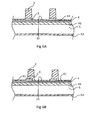
- FIG 1 A shows the cross-section schematic of a typical (prior art) semiconductor-based light detection device, represented by a multi-junction solar cell 100.
- the entire device is depicted, but the method according to the invention is performed only on the top and affects only the cap region 3 and the front surface field (FSF) region 4, which are the top regions of a multi-junction epitaxy grown on a semiconductor substrate 5.
- the solar cell 100 shown in FIG 1A consists of three sub-cells (junctions) 106-108 that are connected through tunnel junctions 167 and 178. It is to be understood that FIG 1 A is merely an example of a typical multi-junction solar cell and that such solar cells may comprise any number of sub-cells.
- FIG 1B is a simplified schematic of a typical (prior art) multi-junction solar cell which only shows the top epitaxial regions relevant to this patent.
- the FSF region 4 is the window region that faces the sun after cap etch. Underneath the FSF region 4 is the emitter region 102 of the top p-n junction 106 that forms a diode. Similar junctions 107 and 108 are disposed below the top p-n junction thus forming a multi-junction cell.
- the FSF region 4 has an important function for the performance in the device. For example, since multi-junction solar cells are minority carrier-type devices, the minority carriers generated through photoabsorption in the emitter region 102 of the top junction 106 must diffuse into the depletion region 103 in order to be collected at the base 104.
- the function of the FSF region 4 is thus to improve the quality of passivation on the surface region 102 and to reduce the surface recombination velocity by reflecting back the minority carriers that diffuse away from the depletion region 103.
- the FSF region 4 is a thin (usually 10 nm to 50 nm) epitaxial region. In addition to improving the collection of the carriers generated in the emitter region 102, the FSF region 4 is usually an absorbing region. The photogenerated minority carriers in the FSF 4 diffuse through the emitter region 102 to the depletion region 103 of the top junction 106 to be collected. Consequently, protection of the top surface 14 of the FSF 4 is important for improving the collection of the minority carriers in the FSF 4.
- the FSF region 4 becomes exposed to a variety of conditions in the process flow subsequent to the cap etch step. These conditions may include, but are not limited to:
- problems are caused by grid metal that comes into direct contact with the FSF region 4.
- the metal grid 2 is deposited while the FSF 4 is exposed
- silver/metal particles may find their way into the exposed FSF and propagate into the p-n junction regions underneath the FSF, rendering the solar cell useless.
- misalignment of the metal grid pattern 2 with respect to the cap grid pattern 3 due to lithographical inaccuracy can result in direct contact between the metal 2 and the FSF 4.
- the portion of the metal 6 on the FSF 4 may result in metal spikes into the junctions during high temperature process steps, resulting in non-operational devices.
- FIG 3 compares the IV characteristics of two different solar cells.
- IV curve 9 is from a high-performance solar cell with no alignment problems
- IV curve 8 shows a shunted current-voltage characteristics resulting from misalignment of the metal grid.
- the cap grid width is typically chosen to be larger than the metal grid width for lithographical misalignment tolerance. A wider cap width negatively affects the performance of the solar cell by increasing the shadowing loss and reducing the current that can be extracted. Consequently there is a need to eliminate metal contact with the FSF surface without increasing the shadowing loss.
- ARC 1 is usually a stack of thin films of dielectrics, the refractive indices of which are chosen to minimize the reflection of sunlight over a desired wavelength range.
- the collective ARC 1 region is required to cover the entire surface of the semiconductor facing the sun, i.e., including the FSF.
- the gridlines were typically also covered during ARC deposition.
- ARC on busbars must be opened to allow for wirebonding, however. This process step is called contact opening and is typically realized using a separate, additional photolithography step.
- the ARC deposition and patterning may be performed at different stages and hence there is no specific requirement to realize this step in a particular order within the process flow.
- a method for making a semiconductor light detection device in which the cap etch and anti-reflection coating steps are performed using a single, self-aligning lithography module.
- the steps are performed in such an order as to minimize exposure of the front surface field region to contaminants and to assure metal to cap region alignment so that the metallized contact regions on top minimally blocks incident light.
- Photoresist is patterned with a cap etch pattern on a provided substrate incorporating epitaxy of a semiconductor light detection device. Subsequently, the cap region is etched, and anti-reflection coating (ARC) is deposited without removing the photoresist. Lastly, the photoresist is removed, henceforth lifting-off the ARC over the defined cap regions.
- the invention is particularly applicable to the manufacture of high-powered light detection devices such as high-efficiency solar cells.
- FIGURE 1A is across-sectional diagram of a multi-junction solar cell in which the invention could be used.
- FIGURE 1B is a simplified version of Figure 1A .
- FIGURE 2 is a cross-sectional diagram of a portion of a prior art cell in which the cap and metal are misaligned.
- FIGURE 3 is a graph of performance of a prior art solar cell in comparison with an ideal cell.
- FIGURES 4A-4E illustrate the process steps according to the invention.
- FIGURE 5 is an illustration of an alternative embodiment of a structure made according to the invention.
- FIGURES 6A-6B are cross-sectional diagrams illustrating perfectly aligned and an imperfectly aligned cells with FSF region protection according to the invention.
- FIGURES 7A-7B are cross-sectional diagrams illustrating oversized metal over a cap in accordance with the invention.
- FIGURE 8 is a cross-sectional diagram showing an alternative embodiment of a device made according to the invention.
- FIG 4A through FIG 4E The main process steps according to the invention are given in FIG 4A through FIG 4E .
- the order of the process steps listed above is critical.
- the remaining process steps, however, can be designed and executed in a variety of ways.
- the present invention is a "process module" of process steps that can be inserted into other process flows as necessary.
- the intervening steps, before the module or after the module can be conventional semiconductor processing steps.
- the order of steps between the epitaxial growth and dicing steps can be changed as necessary, and other steps may be added to the flow.
- the subcells (junctions) forming the solar cell are serially connected through the epitaxy and the metal grid makes a top contact to the top junction and the bottom junction is contacted through the substrate by backside metal 52.
- the present invention is more generally applicable anytime contacts are made to light detection devices from the front side of the substrate, including cases where junctions in a multi-junction solar cell are contacted individually to make multi-terminal solar cell devices.
- the process flow for such devices is generally more complicated and includes more steps.
- the process module as described by the present invention can be used to make top contacts.
- the cap etching and subsequent anti reflection coating steps can be inserted at a desired point in the full process flow.
- the cap etch and subsequent anti reflection coating steps are the first steps in semiconductor processing after the epitaxial growth of the junctions. Subsequently, metal grids are patterned using lift-off. Following metallization, mesa isolation etch is done. The process is finalized with back metallization and dicing.
- the self-aligned nature of the invention allows multiple configurations of the widths of the cap and the metal grid.
- the width of the cap 3 is chosen to be wider than the width of the metal grid 2.
- the grid shadowing is determined by the cap width rather than the metal width.
- the anti-reflection coating 11 will act as an electrically isolating barrier between the metal falling outside of the cap 3 and the FSF 4.
- the width of the cap 3 is chosen to be the same as the width of the metal grid 2.
- the shadowing loss is determined by the metal grid width (and misalignment) and the light detection device can be designed to reflect the optimum performance.
- misalignment as shown in FIG 6B , the anti reflection coating 41 will act as an insulating cap and there will be no electrical conduction between the grid line 2 and the window region 4.
- the width of the cap 3 is chosen to be narrower than the width of the metal grid 2.
- the anti-reflection coating 41 acts as an insulating barrier between the FSF and the metal.
- the total shadowing loss is determined by the width of the metal grids. The advantage of this embodiment is that, even in the case of misalignment as shown in FIG 7B , the shadowing loss will still be determined by the width of the metal grids 2.
- FIG 8 shows another embodiment in which suboptimal process conditions resulted in stray metal clusters 22 depositing near gridlines 12.
- the self-aligned anti reflection coating 31 provides electrical insulation and also acts as a physical barrier between these particles and the FSF 4.
Landscapes
- Photovoltaic Devices (AREA)
- Life Sciences & Earth Sciences (AREA)
- Engineering & Computer Science (AREA)
- Sustainable Development (AREA)
- Sustainable Energy (AREA)
- Light Receiving Elements (AREA)
Applications Claiming Priority (1)
| Application Number | Priority Date | Filing Date | Title |
|---|---|---|---|
| US13/283,379 US8912617B2 (en) | 2011-10-27 | 2011-10-27 | Method for making semiconductor light detection devices |
Publications (2)
| Publication Number | Publication Date |
|---|---|
| EP2587554A2 true EP2587554A2 (de) | 2013-05-01 |
| EP2587554A3 EP2587554A3 (de) | 2015-08-26 |
Family
ID=47216167
Family Applications (1)
| Application Number | Title | Priority Date | Filing Date |
|---|---|---|---|
| EP12250166.1A Withdrawn EP2587554A3 (de) | 2011-10-27 | 2012-10-29 | Verfahren zur Herstellung von Halbleiter-Lichtempfidlichensvorrichtungen |
Country Status (5)
| Country | Link |
|---|---|
| US (1) | US8912617B2 (de) |
| EP (1) | EP2587554A3 (de) |
| JP (1) | JP2013098564A (de) |
| CN (1) | CN103094412A (de) |
| TW (1) | TW201318030A (de) |
Families Citing this family (8)
| Publication number | Priority date | Publication date | Assignee | Title |
|---|---|---|---|---|
| US9263611B2 (en) | 2011-11-17 | 2016-02-16 | Solar Junction Corporation | Method for etching multi-layer epitaxial material |
| US9385169B2 (en) * | 2011-11-29 | 2016-07-05 | Ignis Innovation Inc. | Multi-functional active matrix organic light-emitting diode display |
| US9142615B2 (en) | 2012-10-10 | 2015-09-22 | Solar Junction Corporation | Methods and apparatus for identifying and reducing semiconductor failures |
| DE102015006379B4 (de) * | 2015-05-18 | 2022-03-17 | Azur Space Solar Power Gmbh | Skalierbare Spannungsquelle |
| JP7090400B2 (ja) | 2017-03-08 | 2022-06-24 | 浜松ホトニクス株式会社 | 半導体光検出素子 |
| DE102018110954A1 (de) * | 2018-05-07 | 2019-11-07 | Optics Balzers Ag | Lift-Off Verfahren mittels Jetten |
| US12100772B2 (en) * | 2019-06-04 | 2024-09-24 | The Boeing Company | Solar cell design that minimizes weld attrition and gridline shadowing losses |
| US12245444B2 (en) * | 2021-09-29 | 2025-03-04 | The Boeing Company | Upright photovoltaic cell with front contacts |
Family Cites Families (7)
| Publication number | Priority date | Publication date | Assignee | Title |
|---|---|---|---|---|
| US4838952A (en) | 1988-04-29 | 1989-06-13 | Spectrolab, Inc. | Controlled reflectance solar cell |
| US5330585A (en) * | 1992-10-30 | 1994-07-19 | Spectrolab, Inc. | Gallium arsenide/aluminum gallium arsenide photocell including environmentally sealed ohmic contact grid interface and method of fabricating the cell |
| JP2008282926A (ja) | 2007-05-09 | 2008-11-20 | Sanyo Electric Co Ltd | 太陽電池モジュール |
| DE102008051521A1 (de) * | 2008-10-13 | 2010-04-22 | Helmholtz-Zentrum Berlin Für Materialien Und Energie Gmbh | Verfahren zur Herstellung einer waferbasierten, rückseitenkontaktierten Hetero-Solarzelle und mit dem Verfahren hergestellte Hetero-Solarzelle |
| US20110303281A1 (en) * | 2009-02-26 | 2011-12-15 | Tomoya Kodama | Method for manufacturing thin film compound solar cell |
| US8115097B2 (en) | 2009-11-19 | 2012-02-14 | International Business Machines Corporation | Grid-line-free contact for a photovoltaic cell |
| KR101197945B1 (ko) * | 2010-07-21 | 2012-11-05 | 삼성전기주식회사 | 잉크젯 프린트 헤드 및 그 제조방법 |
-
2011
- 2011-10-27 US US13/283,379 patent/US8912617B2/en active Active
-
2012
- 2012-10-26 CN CN2012104153331A patent/CN103094412A/zh active Pending
- 2012-10-29 JP JP2012237501A patent/JP2013098564A/ja active Pending
- 2012-10-29 TW TW101140005A patent/TW201318030A/zh unknown
- 2012-10-29 EP EP12250166.1A patent/EP2587554A3/de not_active Withdrawn
Non-Patent Citations (1)
| Title |
|---|
| D. DANZILIO ET AL.: "Overview of EMCORE's Multi-junction Solar Cell Technology and High Volume Manufacturing Capabilities", CS MANTECH CONFERENCE, 14 May 2007 (2007-05-14) |
Also Published As
| Publication number | Publication date |
|---|---|
| US20130105930A1 (en) | 2013-05-02 |
| JP2013098564A (ja) | 2013-05-20 |
| TW201318030A (zh) | 2013-05-01 |
| CN103094412A (zh) | 2013-05-08 |
| US8912617B2 (en) | 2014-12-16 |
| EP2587554A3 (de) | 2015-08-26 |
Similar Documents
| Publication | Publication Date | Title |
|---|---|---|
| US8912617B2 (en) | Method for making semiconductor light detection devices | |
| EP3465770B1 (de) | Oberflächenmontierte solarzelle mit integriertem deckglas | |
| KR101991767B1 (ko) | 넓은 밴드갭 반도체 재료를 갖는 이미터 영역을 구비한 태양 전지 | |
| EP3349253B1 (de) | Halbleiterbauelemente und verfahren zur herstellung davon | |
| US10680122B2 (en) | Solar cell and method for manufacturing the same | |
| KR102710224B1 (ko) | 전하-캐리어-선택적 접촉을 통해 연결되는 복수의 흡수체들을 구비한 태양 전지 | |
| US10090428B2 (en) | Solar cell and method for manufacturing the same | |
| EP0595634B1 (de) | Photozelle aus GaAs/AlGaAs bestehend aus einer umgebungsdichten Schnittstelle zwischen Gitter und ohmischen Kontakt, und Verfahren zu deren Herstellung | |
| US8883552B2 (en) | MWT architecture for thin SI solar cells | |
| KR101826912B1 (ko) | 광전변환소자 및 그 제조 방법 | |
| US20140196779A1 (en) | Multi-junction solar cells with through-substrate vias | |
| US10090420B2 (en) | Via etch method for back contact multijunction solar cells | |
| US20100240169A1 (en) | Method to make electrical contact to a bonded face of a photovoltaic cell | |
| US20120298175A1 (en) | Solar panel module and method for manufacturing such a solar panel module | |
| US20150206997A1 (en) | Multi-junction solar cells with recessed through-substrate vias | |
| US20120000506A1 (en) | Photovoltaic module and method of manufacturing the same | |
| JP6021392B2 (ja) | 光電変換装置の製造方法 | |
| KR101714779B1 (ko) | 태양전지 및 이의 제조 방법 | |
| KR20120032238A (ko) | 양면 수광형 태양전지 모듈 | |
| US20100224238A1 (en) | Photovoltaic cell comprising an mis-type tunnel diode | |
| WO2015138764A1 (en) | Multi-junction solar cells with through-substrate vias | |
| WO2014144897A1 (en) | Multi-junction solar cells with through-substrate vias | |
| US8921686B2 (en) | Back-contact photovoltaic cell comprising a thin lamina having a superstrate receiver element | |
| KR20120034964A (ko) | 기판, 상기 기판을 포함하는 태양 전지 및 이들의 제조 방법 | |
| KR101755624B1 (ko) | 태양 전지의 제조 방법 |
Legal Events
| Date | Code | Title | Description |
|---|---|---|---|
| PUAI | Public reference made under article 153(3) epc to a published international application that has entered the european phase |
Free format text: ORIGINAL CODE: 0009012 |
|
| AK | Designated contracting states |
Kind code of ref document: A2 Designated state(s): AL AT BE BG CH CY CZ DE DK EE ES FI FR GB GR HR HU IE IS IT LI LT LU LV MC MK MT NL NO PL PT RO RS SE SI SK SM TR |
|
| AX | Request for extension of the european patent |
Extension state: BA ME |
|
| PUAL | Search report despatched |
Free format text: ORIGINAL CODE: 0009013 |
|
| AK | Designated contracting states |
Kind code of ref document: A3 Designated state(s): AL AT BE BG CH CY CZ DE DK EE ES FI FR GB GR HR HU IE IS IT LI LT LU LV MC MK MT NL NO PL PT RO RS SE SI SK SM TR |
|
| AX | Request for extension of the european patent |
Extension state: BA ME |
|
| RIC1 | Information provided on ipc code assigned before grant |
Ipc: H01L 31/18 20060101ALI20150721BHEP Ipc: H01L 31/0687 20120101AFI20150721BHEP Ipc: H01L 31/0216 20140101ALI20150721BHEP Ipc: H01L 31/0224 20060101ALI20150721BHEP |
|
| STAA | Information on the status of an ep patent application or granted ep patent |
Free format text: STATUS: THE APPLICATION HAS BEEN WITHDRAWN |
|
| 18W | Application withdrawn |
Effective date: 20160205 |