EP2587596A2 - Ensemble avancé de connecteur micro-électronique et procédé de fabrication - Google Patents
Ensemble avancé de connecteur micro-électronique et procédé de fabrication Download PDFInfo
- Publication number
- EP2587596A2 EP2587596A2 EP13152761.6A EP13152761A EP2587596A2 EP 2587596 A2 EP2587596 A2 EP 2587596A2 EP 13152761 A EP13152761 A EP 13152761A EP 2587596 A2 EP2587596 A2 EP 2587596A2
- Authority
- EP
- European Patent Office
- Prior art keywords
- connector
- assembly
- connector assembly
- conductors
- substrate
- Prior art date
- Legal status (The legal status is an assumption and is not a legal conclusion. Google has not performed a legal analysis and makes no representation as to the accuracy of the status listed.)
- Withdrawn
Links
- 238000004519 manufacturing process Methods 0.000 title abstract description 26
- 238000004377 microelectronic Methods 0.000 title description 5
- 239000000758 substrate Substances 0.000 claims abstract description 140
- 239000004020 conductor Substances 0.000 claims description 170
- 230000013011 mating Effects 0.000 claims description 11
- 230000007246 mechanism Effects 0.000 claims description 9
- 230000037361 pathway Effects 0.000 claims description 8
- 230000000717 retained effect Effects 0.000 claims description 7
- 238000000034 method Methods 0.000 abstract description 32
- 230000003750 conditioning effect Effects 0.000 abstract description 5
- 230000005291 magnetic effect Effects 0.000 abstract description 5
- 230000000712 assembly Effects 0.000 description 34
- 238000000429 assembly Methods 0.000 description 34
- 230000003287 optical effect Effects 0.000 description 19
- 238000013459 approach Methods 0.000 description 14
- 239000000853 adhesive Substances 0.000 description 12
- 230000001070 adhesive effect Effects 0.000 description 12
- 239000010410 layer Substances 0.000 description 12
- 239000000463 material Substances 0.000 description 12
- 238000003491 array Methods 0.000 description 8
- ORQBXQOJMQIAOY-UHFFFAOYSA-N nobelium Chemical compound [No] ORQBXQOJMQIAOY-UHFFFAOYSA-N 0.000 description 8
- 230000008569 process Effects 0.000 description 8
- 238000000926 separation method Methods 0.000 description 7
- 230000005540 biological transmission Effects 0.000 description 6
- 238000003780 insertion Methods 0.000 description 6
- 230000037431 insertion Effects 0.000 description 6
- 229920000642 polymer Polymers 0.000 description 6
- 230000008901 benefit Effects 0.000 description 5
- 230000015572 biosynthetic process Effects 0.000 description 5
- 238000013461 design Methods 0.000 description 5
- 239000011152 fibreglass Substances 0.000 description 5
- PXHVJJICTQNCMI-UHFFFAOYSA-N Nickel Chemical compound [Ni] PXHVJJICTQNCMI-UHFFFAOYSA-N 0.000 description 4
- 230000000295 complement effect Effects 0.000 description 4
- 238000010276 construction Methods 0.000 description 4
- 238000001746 injection moulding Methods 0.000 description 4
- RYGMFSIKBFXOCR-UHFFFAOYSA-N Copper Chemical compound [Cu] RYGMFSIKBFXOCR-UHFFFAOYSA-N 0.000 description 3
- 239000003990 capacitor Substances 0.000 description 3
- 238000004891 communication Methods 0.000 description 3
- 239000010949 copper Substances 0.000 description 3
- 230000008878 coupling Effects 0.000 description 3
- 238000010168 coupling process Methods 0.000 description 3
- 238000005859 coupling reaction Methods 0.000 description 3
- 239000008393 encapsulating agent Substances 0.000 description 3
- 230000005496 eutectics Effects 0.000 description 3
- 238000000465 moulding Methods 0.000 description 3
- 239000013307 optical fiber Substances 0.000 description 3
- 229910000679 solder Inorganic materials 0.000 description 3
- 229910000881 Cu alloy Inorganic materials 0.000 description 2
- XUIMIQQOPSSXEZ-UHFFFAOYSA-N Silicon Chemical compound [Si] XUIMIQQOPSSXEZ-UHFFFAOYSA-N 0.000 description 2
- 229910001297 Zn alloy Inorganic materials 0.000 description 2
- 229910052802 copper Inorganic materials 0.000 description 2
- TVZPLCNGKSPOJA-UHFFFAOYSA-N copper zinc Chemical compound [Cu].[Zn] TVZPLCNGKSPOJA-UHFFFAOYSA-N 0.000 description 2
- 230000002939 deleterious effect Effects 0.000 description 2
- 238000005516 engineering process Methods 0.000 description 2
- 238000002955 isolation Methods 0.000 description 2
- 230000000116 mitigating effect Effects 0.000 description 2
- 238000012986 modification Methods 0.000 description 2
- 230000004048 modification Effects 0.000 description 2
- 229910052759 nickel Inorganic materials 0.000 description 2
- 238000012545 processing Methods 0.000 description 2
- 229910052710 silicon Inorganic materials 0.000 description 2
- 239000010703 silicon Substances 0.000 description 2
- 239000002356 single layer Substances 0.000 description 2
- 239000000243 solution Substances 0.000 description 2
- 230000000007 visual effect Effects 0.000 description 2
- 229910000838 Al alloy Inorganic materials 0.000 description 1
- 239000004642 Polyimide Substances 0.000 description 1
- 238000009825 accumulation Methods 0.000 description 1
- 230000004075 alteration Effects 0.000 description 1
- 230000003466 anti-cipated effect Effects 0.000 description 1
- 238000005452 bending Methods 0.000 description 1
- 239000011248 coating agent Substances 0.000 description 1
- 238000000576 coating method Methods 0.000 description 1
- 238000011109 contamination Methods 0.000 description 1
- 230000001066 destructive effect Effects 0.000 description 1
- 238000010586 diagram Methods 0.000 description 1
- 235000019800 disodium phosphate Nutrition 0.000 description 1
- 239000006185 dispersion Substances 0.000 description 1
- 238000006073 displacement reaction Methods 0.000 description 1
- 230000000694 effects Effects 0.000 description 1
- 238000005421 electrostatic potential Methods 0.000 description 1
- 239000000835 fiber Substances 0.000 description 1
- 238000001914 filtration Methods 0.000 description 1
- 230000001939 inductive effect Effects 0.000 description 1
- 239000007924 injection Substances 0.000 description 1
- 238000009434 installation Methods 0.000 description 1
- 230000003993 interaction Effects 0.000 description 1
- 239000004973 liquid crystal related substance Substances 0.000 description 1
- 230000014759 maintenance of location Effects 0.000 description 1
- UXOUKMQIEVGVLY-UHFFFAOYSA-N morin Natural products OC1=CC(O)=CC(C2=C(C(=O)C3=C(O)C=C(O)C=C3O2)O)=C1 UXOUKMQIEVGVLY-UHFFFAOYSA-N 0.000 description 1
- 230000006855 networking Effects 0.000 description 1
- 239000003973 paint Substances 0.000 description 1
- 230000035515 penetration Effects 0.000 description 1
- 229920001721 polyimide Polymers 0.000 description 1
- 238000002360 preparation method Methods 0.000 description 1
- 230000000750 progressive effect Effects 0.000 description 1
- 239000000523 sample Substances 0.000 description 1
- 238000005070 sampling Methods 0.000 description 1
- 238000005476 soldering Methods 0.000 description 1
- 238000006467 substitution reaction Methods 0.000 description 1
- 229920001169 thermoplastic Polymers 0.000 description 1
- 239000004416 thermosoftening plastic Substances 0.000 description 1
- 239000010409 thin film Substances 0.000 description 1
- 229910001174 tin-lead alloy Inorganic materials 0.000 description 1
- 238000012546 transfer Methods 0.000 description 1
- 238000001721 transfer moulding Methods 0.000 description 1
- 230000009466 transformation Effects 0.000 description 1
- 239000012780 transparent material Substances 0.000 description 1
Images











Classifications
-
- H—ELECTRICITY
- H01—ELECTRIC ELEMENTS
- H01R—ELECTRICALLY-CONDUCTIVE CONNECTIONS; STRUCTURAL ASSOCIATIONS OF A PLURALITY OF MUTUALLY-INSULATED ELECTRICAL CONNECTING ELEMENTS; COUPLING DEVICES; CURRENT COLLECTORS
- H01R24/00—Two-part coupling devices, or either of their cooperating parts, characterised by their overall structure
- H01R24/60—Contacts spaced along planar side wall transverse to longitudinal axis of engagement
- H01R24/62—Sliding engagements with one side only, e.g. modular jack coupling devices
- H01R24/64—Sliding engagements with one side only, e.g. modular jack coupling devices for high frequency, e.g. RJ 45
-
- H—ELECTRICITY
- H01—ELECTRIC ELEMENTS
- H01R—ELECTRICALLY-CONDUCTIVE CONNECTIONS; STRUCTURAL ASSOCIATIONS OF A PLURALITY OF MUTUALLY-INSULATED ELECTRICAL CONNECTING ELEMENTS; COUPLING DEVICES; CURRENT COLLECTORS
- H01R13/00—Details of coupling devices of the kinds covered by groups H01R12/70 or H01R24/00 - H01R33/00
- H01R13/46—Bases; Cases
- H01R13/514—Bases; Cases composed as a modular blocks or assembly, i.e. composed of co-operating parts provided with contact members or holding contact members between them
-
- H—ELECTRICITY
- H01—ELECTRIC ELEMENTS
- H01R—ELECTRICALLY-CONDUCTIVE CONNECTIONS; STRUCTURAL ASSOCIATIONS OF A PLURALITY OF MUTUALLY-INSULATED ELECTRICAL CONNECTING ELEMENTS; COUPLING DEVICES; CURRENT COLLECTORS
- H01R13/00—Details of coupling devices of the kinds covered by groups H01R12/70 or H01R24/00 - H01R33/00
- H01R13/66—Structural association with built-in electrical component
- H01R13/717—Structural association with built-in electrical component with built-in light source
- H01R13/7172—Conduits for light transmission
-
- H—ELECTRICITY
- H01—ELECTRIC ELEMENTS
- H01R—ELECTRICALLY-CONDUCTIVE CONNECTIONS; STRUCTURAL ASSOCIATIONS OF A PLURALITY OF MUTUALLY-INSULATED ELECTRICAL CONNECTING ELEMENTS; COUPLING DEVICES; CURRENT COLLECTORS
- H01R13/00—Details of coupling devices of the kinds covered by groups H01R12/70 or H01R24/00 - H01R33/00
- H01R13/66—Structural association with built-in electrical component
- H01R13/6608—Structural association with built-in electrical component with built-in single component
- H01R13/6633—Structural association with built-in electrical component with built-in single component with inductive component, e.g. transformer
-
- H—ELECTRICITY
- H01—ELECTRIC ELEMENTS
- H01R—ELECTRICALLY-CONDUCTIVE CONNECTIONS; STRUCTURAL ASSOCIATIONS OF A PLURALITY OF MUTUALLY-INSULATED ELECTRICAL CONNECTING ELEMENTS; COUPLING DEVICES; CURRENT COLLECTORS
- H01R13/00—Details of coupling devices of the kinds covered by groups H01R12/70 or H01R24/00 - H01R33/00
- H01R13/66—Structural association with built-in electrical component
- H01R13/665—Structural association with built-in electrical component with built-in electronic circuit
- H01R13/6658—Structural association with built-in electrical component with built-in electronic circuit on printed circuit board
-
- H—ELECTRICITY
- H01—ELECTRIC ELEMENTS
- H01R—ELECTRICALLY-CONDUCTIVE CONNECTIONS; STRUCTURAL ASSOCIATIONS OF A PLURALITY OF MUTUALLY-INSULATED ELECTRICAL CONNECTING ELEMENTS; COUPLING DEVICES; CURRENT COLLECTORS
- H01R13/00—Details of coupling devices of the kinds covered by groups H01R12/70 or H01R24/00 - H01R33/00
- H01R13/66—Structural association with built-in electrical component
- H01R13/717—Structural association with built-in electrical component with built-in light source
- H01R13/7175—Light emitting diodes (LEDs)
-
- H—ELECTRICITY
- H01—ELECTRIC ELEMENTS
- H01R—ELECTRICALLY-CONDUCTIVE CONNECTIONS; STRUCTURAL ASSOCIATIONS OF A PLURALITY OF MUTUALLY-INSULATED ELECTRICAL CONNECTING ELEMENTS; COUPLING DEVICES; CURRENT COLLECTORS
- H01R13/00—Details of coupling devices of the kinds covered by groups H01R12/70 or H01R24/00 - H01R33/00
- H01R13/66—Structural association with built-in electrical component
- H01R13/719—Structural association with built-in electrical component specially adapted for high frequency, e.g. with filters
-
- H—ELECTRICITY
- H01—ELECTRIC ELEMENTS
- H01R—ELECTRICALLY-CONDUCTIVE CONNECTIONS; STRUCTURAL ASSOCIATIONS OF A PLURALITY OF MUTUALLY-INSULATED ELECTRICAL CONNECTING ELEMENTS; COUPLING DEVICES; CURRENT COLLECTORS
- H01R13/00—Details of coupling devices of the kinds covered by groups H01R12/70 or H01R24/00 - H01R33/00
- H01R13/66—Structural association with built-in electrical component
- H01R13/719—Structural association with built-in electrical component specially adapted for high frequency, e.g. with filters
- H01R13/7195—Structural association with built-in electrical component specially adapted for high frequency, e.g. with filters with planar filters with openings for contacts
-
- Y—GENERAL TAGGING OF NEW TECHNOLOGICAL DEVELOPMENTS; GENERAL TAGGING OF CROSS-SECTIONAL TECHNOLOGIES SPANNING OVER SEVERAL SECTIONS OF THE IPC; TECHNICAL SUBJECTS COVERED BY FORMER USPC CROSS-REFERENCE ART COLLECTIONS [XRACs] AND DIGESTS
- Y10—TECHNICAL SUBJECTS COVERED BY FORMER USPC
- Y10S—TECHNICAL SUBJECTS COVERED BY FORMER USPC CROSS-REFERENCE ART COLLECTIONS [XRACs] AND DIGESTS
- Y10S439/00—Electrical connectors
- Y10S439/939—Electrical connectors with grounding to metal mounting panel
Definitions
- Prior art connector arrangements relates to their visual indication systems.
- Prior art systems generally use one of two arrangements comprising either LEDs which are directly viewable by the user from the front face of the connector, or optically transmissive conduits (e.g., light pipes) which transfer the light energy from the LED to the front face of the connector.
- a common problem relates to enclosure of the LED within the connector housing (and hence often the external noise shield). This arrangement increases the level of radiated noise within the housing, and therefore the level of noise and cross-talk present in the signal. See for example U.S. Patent No. 6,368,159 issued April 9, 2002 to Hess, et al. . See for example European Patent No. 0878872 to Talend et al.
- an improved connector assembly for use on, inter alia , a printed circuit board or other device.
- the connector includes at least one substrate (e.g., circuit board) disposed in substantially vertical and orthogonal orientation to the front face of the connector.
- the assembly comprises a connector housing having a single port pair (i.e., two modular plug recesses), a plurality of conductors disposed within the recesses for contact with the terminals of the modular plug, and at least one component substrate disposed in the rear portion of the housing, the component substrates having at least one electronic component disposed thereon and in the electrical pathway between the conductors and the corresponding circuit board leads.
- the substantially orthogonal orientation of the board(s) allows maximum space efficiency with minimal noise and cross-talk.
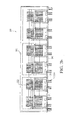
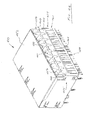
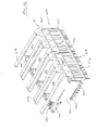
- the assembly 200 generally comprises a connector housing element 202 having a plurality of individual connectors 204 formed therein.
- the connectors 204 are arranged in the illustrated embodiment in side-by-side row fashion within the housing 202 such that two rows 208, 210 of connectors 204 are formed, one disposed atop the other ("row-and-column").
- the front walls 206a of each individual connector 204 are further disposed parallel to one another and generally coplanar, such that modular plugs ( Fig.
- a plurality of grooves 222 which are disposed generally parallel and oriented vertically within the housing 202 are formed generally within the recess 212 of each connector 204 in the housing element 202.
- the grooves 222 are spaced and adapted to guide and receive the aforementioned conductors 220 used to mate with the conductors 216 of the modular plug.
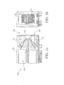
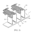
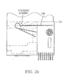
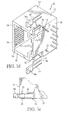
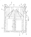
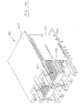
- the conductors 220 are formed in a predetermined shape and held within one of a plurality (e.g., two) of electronic component substrate assemblies 230, 232 ( Fig. 2c ), the latter also mating with the housing element 202 as shown in Fig. 2b .
- the first conductors 220a of the substrate/component assemblies 230, 232 are deformed such that when the assemblies 230, 232 is inserted into its respective cavity 234, the upper conductors 220a are received within the grooves 222, maintained in position to mate with the conductors of the modular plug when the latter is received within the plug recess 212, and also maintained in electrical separation by the separators 223 disposed between and defining the grooves 222.
- the respective primary substrates are in a substantially vertical alignment, and are oriented "face to face" such that the components on each respective substrate are disposed within the cavity for that port pair (see Fig. 2b ).
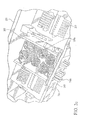
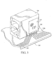
- the recesses 344 formed within the housing element 302 each encompass their respective LED when the latter is inserted therein, and securely hold the LED in place via friction between the LED 303 and the inner walls of the recess (not shown).
- a looser fit and adhesive may be used, or both friction and adhesive.
- the indicator assembly 454 may be mated to the internal substrates 231, 260 of the connector assembly and/or the insert assembly 494 so as to make the inserts 494, substrates 231, 260, and indicator assembly 454 into one unitary assembly. This approach is useful where no external noise shield (or alternatively one which does not impede insertion of the foregoing unitary insert/indicator assembly into the housing) is used.
- the indicator assemblies 454 described herein may be used with other configurations of multi-port connector.
- the disposition and orientation of components internal to the connector are not determinative of the use of the indicator assembly, the latter being able to be adapted to many different connector configurations given the present disclosure and the skill of the ordinary artisan.
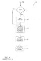
- Fig. 6 the method 600 of manufacturing the aforementioned connector assembly 100 is described in detail. It is noted that while the following description of the method 600 of Fig. 6 is cast in terms of the single port pair connector assembly, the broader method of the invention is equally applicable to other configurations (e.g. , the "row-and-column" embodiment of Fig. 2 ).
Landscapes
- Details Of Connecting Devices For Male And Female Coupling (AREA)
- Connector Housings Or Holding Contact Members (AREA)
- Optical Couplings Of Light Guides (AREA)
- Manufacturing Of Electrical Connectors (AREA)
Applications Claiming Priority (2)
| Application Number | Priority Date | Filing Date | Title |
|---|---|---|---|
| US10/246,840 US6962511B2 (en) | 2001-03-16 | 2002-09-18 | Advanced microelectronic connector assembly and method of manufacturing |
| EP03752601A EP1597751A4 (fr) | 2002-09-18 | 2003-09-17 | Ensemble connecteur microelectronique perfectionne et procede de fabrication correspondant |
Related Parent Applications (1)
| Application Number | Title | Priority Date | Filing Date |
|---|---|---|---|
| EP03752601.9 Division | 2003-09-17 |
Publications (2)
| Publication Number | Publication Date |
|---|---|
| EP2587596A2 true EP2587596A2 (fr) | 2013-05-01 |
| EP2587596A3 EP2587596A3 (fr) | 2013-07-03 |
Family
ID=32028965
Family Applications (2)
| Application Number | Title | Priority Date | Filing Date |
|---|---|---|---|
| EP03752601A Withdrawn EP1597751A4 (fr) | 2002-09-18 | 2003-09-17 | Ensemble connecteur microelectronique perfectionne et procede de fabrication correspondant |
| EP13152761.6A Withdrawn EP2587596A3 (fr) | 2002-09-18 | 2003-09-17 | Ensemble avancé de connecteur micro-électronique et procédé de fabrication |
Family Applications Before (1)
| Application Number | Title | Priority Date | Filing Date |
|---|---|---|---|
| EP03752601A Withdrawn EP1597751A4 (fr) | 2002-09-18 | 2003-09-17 | Ensemble connecteur microelectronique perfectionne et procede de fabrication correspondant |
Country Status (7)
| Country | Link |
|---|---|
| US (1) | US6962511B2 (fr) |
| EP (2) | EP1597751A4 (fr) |
| JP (1) | JP4287374B2 (fr) |
| KR (1) | KR100649810B1 (fr) |
| CN (1) | CN1774842B (fr) |
| AU (1) | AU2003270887A1 (fr) |
| WO (1) | WO2004027835A2 (fr) |
Families Citing this family (50)
| Publication number | Priority date | Publication date | Assignee | Title |
|---|---|---|---|---|
| JP4129195B2 (ja) * | 2003-03-31 | 2008-08-06 | 松下電器産業株式会社 | 蛍光ランプ用点灯装置および電球型蛍光ランプ |
| TW582655U (en) * | 2003-04-17 | 2004-04-01 | Speed Tech Corp | Electrical connector |
| CN105093391B (zh) * | 2004-05-14 | 2022-12-02 | 莫莱克斯公司 | 光导管组件及连接器组件 |
| US7241181B2 (en) | 2004-06-29 | 2007-07-10 | Pulse Engineering, Inc. | Universal connector assembly and method of manufacturing |
| US7029331B1 (en) * | 2005-02-18 | 2006-04-18 | Cheng Uei Precision Industry Co., Ltd. | Shield and connector with the shield |
| US7524206B2 (en) * | 2005-03-23 | 2009-04-28 | Pulse Engineering, Inc. | Power-enabled connector assembly with heat dissipation apparatus and method of manufacturing |
| JP4953682B2 (ja) * | 2006-04-12 | 2012-06-13 | モレックス インコーポレイテド | 表示機能付コネクタ |
| US7125280B1 (en) * | 2006-04-18 | 2006-10-24 | Cheng Uei Precision Industry Co., Ltd. | Electrical connector assembly |
| US7429178B2 (en) | 2006-09-12 | 2008-09-30 | Samtec, Inc. | Modular jack with removable contact array |
| US7519245B2 (en) | 2006-10-31 | 2009-04-14 | Hewlett-Packard Development Company, L.P. | Modular array computer with optical intercell communications pathways |
| WO2008057097A1 (fr) * | 2006-11-10 | 2008-05-15 | Molex Incorporated | Jack modulaire avec boîtier en deux pièces et insert |
| US7285016B1 (en) * | 2006-11-24 | 2007-10-23 | Cheng Uei Precision Industry Co., Ltd. | Connector |
| US7708602B2 (en) * | 2007-03-01 | 2010-05-04 | Pulse Engineering, Inc. | Connector keep-out apparatus and methods |
| US8147278B2 (en) | 2007-03-01 | 2012-04-03 | Pulse Electronics, Inc. | Integrated connector apparatus and methods |
| CN201113016Y (zh) * | 2007-10-09 | 2008-09-10 | 富士康(昆山)电脑接插件有限公司 | 电连接器 |
| JP5098579B2 (ja) * | 2007-10-31 | 2012-12-12 | 株式会社Jvcケンウッド | 電子機器の外部接続コネクタホルダ |
| US7413468B1 (en) | 2007-12-12 | 2008-08-19 | Hon Hai Precision Ind. Co., Ltd. | Connector assembly provided with LED |
| CN201178025Y (zh) * | 2008-01-05 | 2009-01-07 | 富士康(昆山)电脑接插件有限公司 | 磁性线圈模组及设有该模组的电连接器 |
| US8092246B1 (en) | 2008-04-18 | 2012-01-10 | Lockheed Martin Corporation | Self-locking micro-D connector |
| US7845984B2 (en) * | 2008-07-01 | 2010-12-07 | Pulse Engineering, Inc. | Power-enabled connector assembly and method of manufacturing |
| CN201303084Y (zh) * | 2008-07-21 | 2009-09-02 | 富士康(昆山)电脑接插件有限公司 | 电连接器组件 |
| CN101813714B (zh) * | 2009-02-23 | 2012-07-18 | 和舰科技(苏州)有限公司 | 探针装置 |
| US8043109B2 (en) * | 2009-07-27 | 2011-10-25 | Avx Corporation | Wire to board connector |
| US8342884B2 (en) | 2009-07-27 | 2013-01-01 | Avx Corporation | Dual card edge connector with top-loading male and female components |
| US9664711B2 (en) | 2009-07-31 | 2017-05-30 | Pulse Electronics, Inc. | Current sensing devices and methods |
| US9823274B2 (en) | 2009-07-31 | 2017-11-21 | Pulse Electronics, Inc. | Current sensing inductive devices |
| CN105071167B (zh) | 2009-11-06 | 2017-11-24 | 莫列斯公司 | 模块化插座 |
| CN102696154B (zh) | 2009-11-06 | 2015-07-29 | 莫列斯公司 | 连接器 |
| JP2010050110A (ja) * | 2009-12-01 | 2010-03-04 | Japan Aviation Electronics Industry Ltd | コネクタ |
| EP2400294B1 (fr) * | 2010-01-19 | 2014-05-14 | NGK Insulators, Ltd. | Détecteur de gaz et procédé pour sa fabrication |
| CN102237586B (zh) | 2010-04-23 | 2015-11-25 | 富士康(昆山)电脑接插件有限公司 | 电连接器 |
| US8591262B2 (en) | 2010-09-03 | 2013-11-26 | Pulse Electronics, Inc. | Substrate inductive devices and methods |
| WO2013130842A1 (fr) | 2012-03-02 | 2013-09-06 | Pulse Electronics, Inc. | Appareil d'antenne à déposition et procédés |
| US9178318B2 (en) | 2012-04-27 | 2015-11-03 | Pulse Electronics, Inc. | Shielded integrated connector modules and assemblies and methods of manufacturing the same |
| US9304149B2 (en) | 2012-05-31 | 2016-04-05 | Pulse Electronics, Inc. | Current sensing devices and methods |
| US20140125446A1 (en) | 2012-11-07 | 2014-05-08 | Pulse Electronics, Inc. | Substrate inductive device methods and apparatus |
| CN103972743A (zh) | 2013-01-28 | 2014-08-06 | 富士康(昆山)电脑接插件有限公司 | 发光二极管及运用其的电连接器 |
| US9601857B2 (en) | 2013-05-23 | 2017-03-21 | Pulse Electronics, Inc. | Methods and apparatus for terminating wire wound electronic devices |
| US9401561B2 (en) | 2013-07-02 | 2016-07-26 | Pulse Electronics, Inc. | Methods and apparatus for terminating wire wound electronic components to a header assembly |
| US9716344B2 (en) | 2013-07-02 | 2017-07-25 | Pulse Electronics, Inc. | Apparatus for terminating wire wound electronic components to an insert header assembly |
| US10020561B2 (en) | 2013-09-19 | 2018-07-10 | Pulse Finland Oy | Deposited three-dimensional antenna apparatus and methods |
| US9486956B2 (en) * | 2013-09-30 | 2016-11-08 | Apple Inc. | Power adapter components, housing and methods of assembly |
| WO2015125028A2 (fr) | 2014-02-12 | 2015-08-27 | Pulse Finland Oy | Procédés et appareil permettant une formation et un dépôt d'éléments conducteurs |
| TWM484783U (zh) * | 2014-05-07 | 2014-08-21 | Bothhand Entpr Inc | 電子元件座 |
| US9833802B2 (en) | 2014-06-27 | 2017-12-05 | Pulse Finland Oy | Methods and apparatus for conductive element deposition and formation |
| US9397450B1 (en) * | 2015-06-12 | 2016-07-19 | Amphenol Corporation | Electrical connector with port light indicator |
| US9905985B2 (en) * | 2015-06-16 | 2018-02-27 | Lear Corporation | Optimized high current connector pattern for PDB |
| DE202017101914U1 (de) * | 2017-03-31 | 2018-05-02 | Igus Gmbh | Baukastensystem für Steckverbindermodule, Steckverbindereinheit und modulare Gehäuserahmen hierfür |
| JP6955984B2 (ja) * | 2017-12-05 | 2021-10-27 | 東京エレクトロン株式会社 | 基板処理装置、基板処理装置の設置方法及びコンピュータ記憶媒体 |
| DE102018125121A1 (de) | 2018-10-11 | 2020-04-16 | Harting Electric Gmbh & Co. Kg | Steckverbinder |
Family Cites Families (27)
| Publication number | Priority date | Publication date | Assignee | Title |
|---|---|---|---|---|
| US5069641A (en) | 1990-02-03 | 1991-12-03 | Murata Manufacturing Co., Ltd. | Modular jack |
| US5613873A (en) | 1993-12-16 | 1997-03-25 | Dell Usa, L.P. | Modular jack with integral light-emitting diode |
| US5741152A (en) * | 1995-04-25 | 1998-04-21 | Amphenol Corporation | Electrical connector with indicator lights |
| US5876240A (en) * | 1997-04-01 | 1999-03-02 | The Whitaker Corp | Stacked electrical connector with visual indicators |
| US5876239A (en) * | 1996-08-30 | 1999-03-02 | The Whitaker Corporation | Electrical connector having a light indicator |
| US5759067A (en) | 1996-12-11 | 1998-06-02 | Scheer; Peter L. | Shielded connector |
| US5885100A (en) | 1997-05-12 | 1999-03-23 | Molex Incorporated | Electrical connector with light transmission means |
| US6095851A (en) | 1997-11-17 | 2000-08-01 | Xircom, Inc. | Status indicator for electronic device |
| US6174194B1 (en) | 1998-11-09 | 2001-01-16 | Molex Incorporated | Add-on electrical assembly with light transmission means |
| US6116963A (en) | 1998-10-09 | 2000-09-12 | Pulse Engineering, Inc. | Two-piece microelectronic connector and method |
| US6554638B1 (en) | 1998-10-14 | 2003-04-29 | Stewart Connector Systems, Inc. | Modular electrical connector assemblies with magnetic filter and/or visual indicator |
| US6196879B1 (en) | 1998-12-02 | 2001-03-06 | Stewart Connector Systems, Inc. | Surface-mountable modular electrical connector assemblies having co-planar terminals |
| US6457992B2 (en) | 1999-02-08 | 2002-10-01 | 3Com Corporation | Visual feedback system for electronic device |
| US6325664B1 (en) | 1999-03-11 | 2001-12-04 | Pulse Engineering, Inc. | Shielded microelectronic connector with indicators and method of manufacturing |
| US6428361B1 (en) | 1999-05-24 | 2002-08-06 | Stewart Connector Systems, Inc. | Surface mountable connector assembly including a printed circuit board |
| US6132260A (en) | 1999-08-10 | 2000-10-17 | Hon Hai Precision Ind. Co., Ltd. | Modular connector assembly |
| US6193560B1 (en) | 2000-03-03 | 2001-02-27 | Tyco Electronics Corporation | Connector assembly with side-by-side terminal arrays |
| US6483712B1 (en) | 2000-03-20 | 2002-11-19 | 3Com Corporation | Illuminating electrical jack system |
| US6361357B1 (en) | 2000-04-13 | 2002-03-26 | 3Com Corporation | Remotely illuminated electronic connector for improving viewing of status indicators |
| US6325665B1 (en) * | 2000-04-25 | 2001-12-04 | Yu-Lin Chung | Power adapter with cable storage device |
| US6642827B1 (en) | 2000-09-13 | 2003-11-04 | Pulse Engineering | Advanced electronic microminiature coil and method of manufacturing |
| TW464086U (en) | 2000-11-15 | 2001-11-11 | Hon Hai Prec Ind Co Ltd | Electric connector for socket |
| US6585540B2 (en) | 2000-12-06 | 2003-07-01 | Pulse Engineering | Shielded microelectronic connector assembly and method of manufacturing |
| US6368159B1 (en) | 2000-12-13 | 2002-04-09 | Stewart Connector Systems, Inc. | Light pipe for a modular jack |
| TW477479U (en) | 2000-12-21 | 2002-02-21 | Hon Hai Prec Ind Co Ltd | Socket connector |
| US20020146940A1 (en) | 2001-04-10 | 2002-10-10 | Robert Colantuono | Magnetically integrated jack |
| US6773298B2 (en) | 2002-05-06 | 2004-08-10 | Pulse Engineering, Inc. | Connector assembly with light source sub-assemblies and method of manufacturing |
-
2002
- 2002-09-18 US US10/246,840 patent/US6962511B2/en not_active Expired - Lifetime
-
2003
- 2003-09-17 EP EP03752601A patent/EP1597751A4/fr not_active Withdrawn
- 2003-09-17 AU AU2003270887A patent/AU2003270887A1/en not_active Abandoned
- 2003-09-17 CN CN03825137.XA patent/CN1774842B/zh not_active Expired - Fee Related
- 2003-09-17 KR KR1020057004741A patent/KR100649810B1/ko not_active Expired - Fee Related
- 2003-09-17 EP EP13152761.6A patent/EP2587596A3/fr not_active Withdrawn
- 2003-09-17 WO PCT/US2003/030184 patent/WO2004027835A2/fr not_active Ceased
- 2003-09-17 JP JP2004538490A patent/JP4287374B2/ja not_active Expired - Fee Related
Also Published As
| Publication number | Publication date |
|---|---|
| WO2004027835A2 (fr) | 2004-04-01 |
| JP4287374B2 (ja) | 2009-07-01 |
| AU2003270887A8 (en) | 2004-04-08 |
| US6962511B2 (en) | 2005-11-08 |
| JP2006503405A (ja) | 2006-01-26 |
| EP1597751A4 (fr) | 2008-06-25 |
| CN1774842A (zh) | 2006-05-17 |
| KR100649810B1 (ko) | 2006-11-28 |
| KR20050067151A (ko) | 2005-06-30 |
| EP2587596A3 (fr) | 2013-07-03 |
| EP1597751A2 (fr) | 2005-11-23 |
| WO2004027835A3 (fr) | 2005-09-29 |
| CN1774842B (zh) | 2014-06-25 |
| AU2003270887A1 (en) | 2004-04-08 |
| US20040005820A1 (en) | 2004-01-08 |
Similar Documents
| Publication | Publication Date | Title |
|---|---|---|
| US6962511B2 (en) | Advanced microelectronic connector assembly and method of manufacturing | |
| US6773302B2 (en) | Advanced microelectronic connector assembly and method of manufacturing | |
| US6773298B2 (en) | Connector assembly with light source sub-assemblies and method of manufacturing | |
| US6878012B2 (en) | Shielded microelectronic connector assembly and method of manufacturing | |
| US6769936B2 (en) | Connector with insert assembly and method of manufacturing | |
| US8480440B2 (en) | Universal connector assembly and method of manufacturing |
Legal Events
| Date | Code | Title | Description |
|---|---|---|---|
| PUAI | Public reference made under article 153(3) epc to a published international application that has entered the european phase |
Free format text: ORIGINAL CODE: 0009012 |
|
| AC | Divisional application: reference to earlier application |
Ref document number: 1597751 Country of ref document: EP Kind code of ref document: P |
|
| AK | Designated contracting states |
Kind code of ref document: A2 Designated state(s): AT BE BG CH CY CZ DE DK EE ES FI FR GB GR HU IE IT LI LU MC NL PT RO SE SI SK TR |
|
| PUAL | Search report despatched |
Free format text: ORIGINAL CODE: 0009013 |
|
| AK | Designated contracting states |
Kind code of ref document: A3 Designated state(s): AT BE BG CH CY CZ DE DK EE ES FI FR GB GR HU IE IT LI LU MC NL PT RO SE SI SK TR |
|
| RIC1 | Information provided on ipc code assigned before grant |
Ipc: H01R 13/719 20110101ALN20130524BHEP Ipc: H01R 13/66 20060101ALN20130524BHEP Ipc: H01R 24/64 20110101ALI20130524BHEP Ipc: H01R 13/717 20060101AFI20130524BHEP |
|
| RAP1 | Party data changed (applicant data changed or rights of an application transferred) |
Owner name: PULSE ELECTRONICS, INC. |
|
| STAA | Information on the status of an ep patent application or granted ep patent |
Free format text: STATUS: THE APPLICATION IS DEEMED TO BE WITHDRAWN |
|
| 18D | Application deemed to be withdrawn |
Effective date: 20140104 |