EP2587652A1 - Convertisseur continu-continu - Google Patents
Convertisseur continu-continu Download PDFInfo
- Publication number
- EP2587652A1 EP2587652A1 EP10853590.7A EP10853590A EP2587652A1 EP 2587652 A1 EP2587652 A1 EP 2587652A1 EP 10853590 A EP10853590 A EP 10853590A EP 2587652 A1 EP2587652 A1 EP 2587652A1
- Authority
- EP
- European Patent Office
- Prior art keywords
- switching
- mode
- leg
- rectifier circuit
- diode
- Prior art date
- Legal status (The legal status is an assumption and is not a legal conclusion. Google has not performed a legal analysis and makes no representation as to the accuracy of the status listed.)
- Granted
Links
Images







Classifications
-
- H—ELECTRICITY
- H02—GENERATION; CONVERSION OR DISTRIBUTION OF ELECTRIC POWER
- H02M—APPARATUS FOR CONVERSION BETWEEN AC AND AC, BETWEEN AC AND DC, OR BETWEEN DC AND DC, AND FOR USE WITH MAINS OR SIMILAR POWER SUPPLY SYSTEMS; CONVERSION OF DC OR AC INPUT POWER INTO SURGE OUTPUT POWER; CONTROL OR REGULATION THEREOF
- H02M3/00—Conversion of DC power input into DC power output
- H02M3/22—Conversion of DC power input into DC power output with intermediate conversion into AC
- H02M3/24—Conversion of DC power input into DC power output with intermediate conversion into AC by static converters
- H02M3/28—Conversion of DC power input into DC power output with intermediate conversion into AC by static converters using discharge tubes with control electrode or semiconductor devices with control electrode to produce the intermediate AC
- H02M3/325—Conversion of DC power input into DC power output with intermediate conversion into AC by static converters using discharge tubes with control electrode or semiconductor devices with control electrode to produce the intermediate AC using devices of a triode or a transistor type requiring continuous application of a control signal
- H02M3/335—Conversion of DC power input into DC power output with intermediate conversion into AC by static converters using discharge tubes with control electrode or semiconductor devices with control electrode to produce the intermediate AC using devices of a triode or a transistor type requiring continuous application of a control signal using semiconductor devices only
-
- H—ELECTRICITY
- H02—GENERATION; CONVERSION OR DISTRIBUTION OF ELECTRIC POWER
- H02M—APPARATUS FOR CONVERSION BETWEEN AC AND AC, BETWEEN AC AND DC, OR BETWEEN DC AND DC, AND FOR USE WITH MAINS OR SIMILAR POWER SUPPLY SYSTEMS; CONVERSION OF DC OR AC INPUT POWER INTO SURGE OUTPUT POWER; CONTROL OR REGULATION THEREOF
- H02M3/00—Conversion of DC power input into DC power output
- H02M3/22—Conversion of DC power input into DC power output with intermediate conversion into AC
- H02M3/24—Conversion of DC power input into DC power output with intermediate conversion into AC by static converters
- H02M3/28—Conversion of DC power input into DC power output with intermediate conversion into AC by static converters using discharge tubes with control electrode or semiconductor devices with control electrode to produce the intermediate AC
- H02M3/325—Conversion of DC power input into DC power output with intermediate conversion into AC by static converters using discharge tubes with control electrode or semiconductor devices with control electrode to produce the intermediate AC using devices of a triode or a transistor type requiring continuous application of a control signal
- H02M3/335—Conversion of DC power input into DC power output with intermediate conversion into AC by static converters using discharge tubes with control electrode or semiconductor devices with control electrode to produce the intermediate AC using devices of a triode or a transistor type requiring continuous application of a control signal using semiconductor devices only
- H02M3/33507—Conversion of DC power input into DC power output with intermediate conversion into AC by static converters using discharge tubes with control electrode or semiconductor devices with control electrode to produce the intermediate AC using devices of a triode or a transistor type requiring continuous application of a control signal using semiconductor devices only with automatic control of the output voltage or current, e.g. flyback converters
-
- H—ELECTRICITY
- H02—GENERATION; CONVERSION OR DISTRIBUTION OF ELECTRIC POWER
- H02M—APPARATUS FOR CONVERSION BETWEEN AC AND AC, BETWEEN AC AND DC, OR BETWEEN DC AND DC, AND FOR USE WITH MAINS OR SIMILAR POWER SUPPLY SYSTEMS; CONVERSION OF DC OR AC INPUT POWER INTO SURGE OUTPUT POWER; CONTROL OR REGULATION THEREOF
- H02M3/00—Conversion of DC power input into DC power output
- H02M3/22—Conversion of DC power input into DC power output with intermediate conversion into AC
- H02M3/24—Conversion of DC power input into DC power output with intermediate conversion into AC by static converters
-
- H—ELECTRICITY
- H02—GENERATION; CONVERSION OR DISTRIBUTION OF ELECTRIC POWER
- H02M—APPARATUS FOR CONVERSION BETWEEN AC AND AC, BETWEEN AC AND DC, OR BETWEEN DC AND DC, AND FOR USE WITH MAINS OR SIMILAR POWER SUPPLY SYSTEMS; CONVERSION OF DC OR AC INPUT POWER INTO SURGE OUTPUT POWER; CONTROL OR REGULATION THEREOF
- H02M3/00—Conversion of DC power input into DC power output
- H02M3/22—Conversion of DC power input into DC power output with intermediate conversion into AC
- H02M3/24—Conversion of DC power input into DC power output with intermediate conversion into AC by static converters
- H02M3/28—Conversion of DC power input into DC power output with intermediate conversion into AC by static converters using discharge tubes with control electrode or semiconductor devices with control electrode to produce the intermediate AC
-
- H—ELECTRICITY
- H02—GENERATION; CONVERSION OR DISTRIBUTION OF ELECTRIC POWER
- H02M—APPARATUS FOR CONVERSION BETWEEN AC AND AC, BETWEEN AC AND DC, OR BETWEEN DC AND DC, AND FOR USE WITH MAINS OR SIMILAR POWER SUPPLY SYSTEMS; CONVERSION OF DC OR AC INPUT POWER INTO SURGE OUTPUT POWER; CONTROL OR REGULATION THEREOF
- H02M3/00—Conversion of DC power input into DC power output
- H02M3/22—Conversion of DC power input into DC power output with intermediate conversion into AC
- H02M3/24—Conversion of DC power input into DC power output with intermediate conversion into AC by static converters
- H02M3/28—Conversion of DC power input into DC power output with intermediate conversion into AC by static converters using discharge tubes with control electrode or semiconductor devices with control electrode to produce the intermediate AC
- H02M3/325—Conversion of DC power input into DC power output with intermediate conversion into AC by static converters using discharge tubes with control electrode or semiconductor devices with control electrode to produce the intermediate AC using devices of a triode or a transistor type requiring continuous application of a control signal
- H02M3/335—Conversion of DC power input into DC power output with intermediate conversion into AC by static converters using discharge tubes with control electrode or semiconductor devices with control electrode to produce the intermediate AC using devices of a triode or a transistor type requiring continuous application of a control signal using semiconductor devices only
- H02M3/33538—Conversion of DC power input into DC power output with intermediate conversion into AC by static converters using discharge tubes with control electrode or semiconductor devices with control electrode to produce the intermediate AC using devices of a triode or a transistor type requiring continuous application of a control signal using semiconductor devices only of the forward type
-
- H—ELECTRICITY
- H02—GENERATION; CONVERSION OR DISTRIBUTION OF ELECTRIC POWER
- H02M—APPARATUS FOR CONVERSION BETWEEN AC AND AC, BETWEEN AC AND DC, OR BETWEEN DC AND DC, AND FOR USE WITH MAINS OR SIMILAR POWER SUPPLY SYSTEMS; CONVERSION OF DC OR AC INPUT POWER INTO SURGE OUTPUT POWER; CONTROL OR REGULATION THEREOF
- H02M3/00—Conversion of DC power input into DC power output
- H02M3/22—Conversion of DC power input into DC power output with intermediate conversion into AC
- H02M3/24—Conversion of DC power input into DC power output with intermediate conversion into AC by static converters
- H02M3/28—Conversion of DC power input into DC power output with intermediate conversion into AC by static converters using discharge tubes with control electrode or semiconductor devices with control electrode to produce the intermediate AC
- H02M3/325—Conversion of DC power input into DC power output with intermediate conversion into AC by static converters using discharge tubes with control electrode or semiconductor devices with control electrode to produce the intermediate AC using devices of a triode or a transistor type requiring continuous application of a control signal
- H02M3/335—Conversion of DC power input into DC power output with intermediate conversion into AC by static converters using discharge tubes with control electrode or semiconductor devices with control electrode to produce the intermediate AC using devices of a triode or a transistor type requiring continuous application of a control signal using semiconductor devices only
- H02M3/337—Conversion of DC power input into DC power output with intermediate conversion into AC by static converters using discharge tubes with control electrode or semiconductor devices with control electrode to produce the intermediate AC using devices of a triode or a transistor type requiring continuous application of a control signal using semiconductor devices only in push-pull configuration
- H02M3/3376—Conversion of DC power input into DC power output with intermediate conversion into AC by static converters using discharge tubes with control electrode or semiconductor devices with control electrode to produce the intermediate AC using devices of a triode or a transistor type requiring continuous application of a control signal using semiconductor devices only in push-pull configuration with automatic control of output voltage or current
-
- H—ELECTRICITY
- H02—GENERATION; CONVERSION OR DISTRIBUTION OF ELECTRIC POWER
- H02M—APPARATUS FOR CONVERSION BETWEEN AC AND AC, BETWEEN AC AND DC, OR BETWEEN DC AND DC, AND FOR USE WITH MAINS OR SIMILAR POWER SUPPLY SYSTEMS; CONVERSION OF DC OR AC INPUT POWER INTO SURGE OUTPUT POWER; CONTROL OR REGULATION THEREOF
- H02M1/00—Details of apparatus for conversion
- H02M1/0003—Details of control, feedback or regulation circuits
- H02M1/0032—Control circuits allowing low power mode operation, e.g. in standby mode
-
- Y—GENERAL TAGGING OF NEW TECHNOLOGICAL DEVELOPMENTS; GENERAL TAGGING OF CROSS-SECTIONAL TECHNOLOGIES SPANNING OVER SEVERAL SECTIONS OF THE IPC; TECHNICAL SUBJECTS COVERED BY FORMER USPC CROSS-REFERENCE ART COLLECTIONS [XRACs] AND DIGESTS
- Y02—TECHNOLOGIES OR APPLICATIONS FOR MITIGATION OR ADAPTATION AGAINST CLIMATE CHANGE
- Y02B—CLIMATE CHANGE MITIGATION TECHNOLOGIES RELATED TO BUILDINGS, e.g. HOUSING, HOUSE APPLIANCES OR RELATED END-USER APPLICATIONS
- Y02B70/00—Technologies for an efficient end-user side electric power management and consumption
- Y02B70/10—Technologies improving the efficiency by using switched-mode power supplies [SMPS], i.e. efficient power electronics conversion e.g. power factor correction or reduction of losses in power supplies or efficient standby modes
Definitions
- the present invention relates to a DC-DC converter having insulating function.
- a conventionally known DC-DC converter is a device for outputting a power by converting DC power to AC power by a switching circuit, transforming this using a transformer, and converting this to DC power by a rectifier circuit.
- a full bridge circuit In handling large power, it is general that a full bridge circuit is used.
- it became hard switching in turn-on and turn-off of the switching element which generated a large switching loss, resulting in inferior efficiency.
- PATENT DOCUMENT 1 a DC-DC converter to reduce the switching loss and to improve efficiency has been disclosed in PATENT DOCUMENT 1.
- This DC-DC converter is implemented by shifting a phase of on/off drive of one switching element connected in series and on/off drive of the other switching element connected in series, composing the full bridge circuit. In this way, zero voltage switching becomes possible, and reduction of the switching loss is attained.
- This control system is called a phase shift system.
- the full bridge circuit of the phase shift system enables zero voltage switching, in large power supply amount to a load, however, time required in charge-discharge of a parasitic capacitance of the switching element becomes long, due to small current flowing in a circuit, in small power supply amount to a load.
- the DC-DC converter relevant to the present invention is characterized by a full bridge circuit, composed of a first switching leg connecting a first and a second switching elements in series, and a second switching leg connecting a third and a fourth switching elements in series, the first and second switching legs being connected in parallel, wherein DC terminals are provided between both ends of the first switching leg and between both ends of the second switching leg, and AC terminals are provided between the series connecting point of the first and the second switching elements, and the series connecting point of the third and the fourth switching elements; a rectifier circuit having a smoothing reactor; a first smoothing capacitor connected to a DC power source in parallel and connected to the DC terminals of the full bridge circuit; a second smoothing capacitor connected to a load in parallel, and connected to a DC terminals of the rectifier circuit; a primary winding connected to the AC terminals of the full bridge circuit; a secondary winding connected to an AC terminals of the rectifier circuit; a transformer for connecting magnetically the primary winding and the secondary winding; and
- a vehicle relevant to the present invention is characterized by mounting the DC-DC converter of the present invention.
- a highly-efficient DC-DC converter can be provided.
- a vehicle regardless of a power supply amount of to a load, a vehicle, which enables a highly-efficient power supply to a load, can be provided.
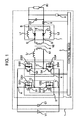
- Fig. 1 is a circuit configuration diagram of the DC-DC converter 1 according to Embodiment 1 of the present invention.
- This DC-DC converter 1 supplies power to a load R1, by transforming the voltage of a DC power source V1. It should be noted that the DC power source V1 may be substituted with output of other converter of a power factor correction circuit or the like.
- the DC power source V1 and a smoothing capacitor C1 are connected between DC terminals A-A' of a full bridge circuit 2.
- a smoothing capacitor C2 and the load R1 are connected between DC terminals B-B of a rectifier circuit 7.
- a primary winding N1 is connected between AC terminals C-C' of full bridge circuit 2
- a secondary winding N2 is connected between AC terminals D-D' of the rectifier circuit 7.
- This primary winding N1 and secondary winding N2 are magnetically connected by a transformer 6.
- the full bridge circuit 2 is composed of a first switching leg 3 connected a first switching element S1 and a second switching element S2 in series, and a second switching leg 4 connected a third switching element S3 and a fourth switching element S4 in series.
- antiparallel diodes DS1 to DS4 are connected, respectively.
- a body diode of MOSFET can be utilized as the antiparallel diode.
- the switching elements S1 to S4 have parasitic capacitance CS1 to CS4.
- a snubber capacitor may be connected to the switching elements S1 to S4 in parallel, as a capacitor.
- MOSFET is used as the switching elements S1 and S2
- IGBT is used as the switching elements S3 and S4.
- a reactor Lr is inserted in series between the AC terminals and the primary winding N1 of the full bridge circuit 2.
- a leak inductance of the transformer 6 may be utilized.
- a rectifier circuit 7 is composed of two smoothing reactors L1 and L2 and two diodes D1 and D2. At one end of the secondary winding N2, one end of the smoothing reactor L1 and a cathode of the diode D2 are connected, and at the other end of the secondary winding N2, one end of the smoothing reactor L2 and a cathode of the diode D1 are connected. The other end of the smoothing reactor L1 and L2 is connected to one end of the smoothing capacitor C2, and an anode of the diode D1 and D2 is connected to the other end of the smoothing capacitor C2.
- the switching element may be used instead of the diode D1 and D2. In this case, adoption of a synchronous rectification system enables to further enhance efficiency of the DC-DC converter 1.
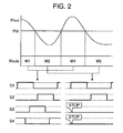
- the DC-DC converter 1 of the present invention is characterized by switching an operating mode of the switching element in response to power supply amount to the load R1. Explanation will be given below on switching of an operating mode with reference to Fig. 2 .
- Fig. 2 is a drawing explaining the switching of operating mode.
- Output power Pout is a product of output current detected by a current sensor 8, and output voltage detected by a voltage sensor 9.
- Pth is a predetermined value set to switch the operating mode.
- the control means 5 drives the switching elements S1 to S4, as the heavy load mode M1, which is the first mode. In this case, when the switching elements S 1 to S4 are driven by the phase shift system, zero voltage switching is possible.
- output power Pout becomes predetermined value Pth or less, it is transferred to the light load mode M2, which is the second mode.
- the control means 5 makes the switching elements S3 and S4 stopped in an OFF state, and drives only the switching elements S 1 and S2.
- the control means 5 controls output power by controlling drive frequency of the switching elements S1 and S2. It should be noted that, in the same drawing, a drive signal for driving the switching elements S 1 to S4 is described at the lower stage of the graph, and the High side represents an ON-signal and the Low side represents an OFF-signal.
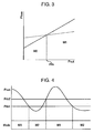
- Fig. 3 is a drawing explaining a determination method for a predetermined value Pth.
- a Ploss-Pout straight line shown by a dotted line shows loss in each output power Pout actuated by the heavy load mode M1
- the Ploss-Pout straight line shown by a solid line shows loss in each output power Pout actuated by the light load mode M2.
- the predetermined value Pth may be determined by size of the output power Pout, so that loss Ploss selects the smaller operating modes M1 and M2. Theoretically, by setting a cross-point of the dotted line and the solid line as Pth, the best efficiency is obtained. Naturally, the predetermined value Pth may be set arbitrarily.
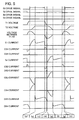
- FIG. 5 is a drawing of a voltage/current waveform explaining the operation in a light load mode M2 of the DC-DC converter 1.
- An S1 drive signal to an S4 drive signal represent a drive signal waveform which the control means 5 outputs to the switching elements S1 to S4, respectively.
- the switching elements S 1 to S4 are made ON, when the drive signal waveform to be output to the switching elements S 1 to S4 becomes High, and are made OFF, when it becomes Low.
- T1 voltage represents a waveform of voltage of the node T1 at one end side of the primary winding N1
- T2 voltage represents a waveform of voltage of the node T2 at the other end side of the primary winding N1.
- Voltage between T1-T2 represents a voltage waveform where T2 voltage is subtracted from T1 voltage. Explanation will be given next on a current waveform in Fig. 5 .
- S1 current and S2 current represent current between drain-source of the switching elements S1 and S2, respectively.
- CS1 current to CS4 current represent a current waveform flowing the parasitic capacitance CS1 to CS4, respectively.
- CS1 current to CS4 current positive current is called charge current, and negative current is called discharge current, provided that flow direction from one end of the parasitic capacitance connected to a drain of the switching element to the other end of the parasitic capacitance connected to a source of the switching element is positive.
- DS1 current to DS4 current represent a current waveform flowing the antiparallel diodes DS1 to DS4, respectively.
- a direction flowing from an anode to a cathode is set to be positive, in antiparallel diodes DS1 to DS4, respectively.
- periods (a) to (h) partitioned by each dotted line in Fig. 5 correspond to the (mode a) to the (mode h), to be explained below, respectively.
- drive signals of the switching elements S3 and S4 become OFF over all modes of the (mode a) to the (mode h).
- Fig. 6 is a circuit diagram explaining an operation (mode a) in a light load mode M2 in the period (a) shown in Fig. 5 .
- the switching element S1 is turned-ON. Voltage between the both ends of the switching element S1 is zero voltage due to conduction of the antiparallel diode DS1, and thus the switching element S1 becomes zero voltage switching. After that, when current flowing the reactor Lr comes up to zero, reverse recovery current flows, which is current till reverse recovery to the antiparallel diode DS4, and current flowing the reactor Lr increases in a positive direction. After that, when the antiparallel diode DS4 attains reverse recovery, current flowing the switching element S1 becomes charge current of the parasitic capacitance CS4 and discharge current of the parasitic capacitance CS3.
- Fig. 7 is a circuit diagram explaining an operation (mode b) in a light load mode M2 in the period (b) shown in Fig. 5 .
- Discharge of the parasitic capacitance CS3 decreases both ends voltage of the antiparallel diode DS3, and crossing the zero voltage conducts the antiparallel diode DS3.
- Conduction of the antiparallel diode DS3 inhibits flow of discharge current of the parasitic capacitance CS3 and charge current of the parasitic capacitance CS4.
- Current flowed the antiparallel diode DS3 returns to the antiparallel diode DS3 through the switching element S1, the reactor Lr and the primary winding N1. Current flowing this route increases gradually.
- Fig. 8 is a circuit diagram explaining an operation (mode c) in a light load mode M2 in the period (c) shown in Fig. 5 .
- the switching element S1 is turned-OFF.
- Current flowing the antiparallel diode DS3 becomes charge current to the parasitic capacitance CS1 and discharge current of the parasitic capacitance CS2.
- Discharge of the parasitic capacitance CS2 decreases voltage of the node T1, however, voltage of the node T2 maintains higher voltage than the DC voltage V1 due to conduction of the antiparallel diode DS3. In this way, voltage between the node T1 and the node T2 enlarges in a negative direction.
- Fig. 9 is a circuit diagram explaining an operation (mode d) in a light load mode M2 in the period (d) shown in Fig. 5 .
- Discharge of the parasitic capacitance CS2 decreases both ends voltage of the antiparallel diode DS2, and crossing the zero voltage conducts the antiparallel diode DS2.
- Conduction of the antiparallel diode DS2 inhibits flow of discharge current of the parasitic capacitance CS2 and charge current of the parasitic capacitance CS1.
- Current flowed the antiparallel diode DS2 returns to the antiparallel diode DS2 through the reactor Lr and the primary winding N1. Current flowing this route increases gradually.
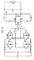
- Fig. 10 is a circuit diagram explaining an operation (mode e) in a light load mode M2 in the period (e) shown in Fig. 5 .
- the switching element S2 is turned-ON. Voltage between the both ends of the switching element S2 is zero voltage due to conduction of the antiparallel diode DS2, and thus the switching element S2 becomes zero voltage switching. After that, when current flowing the reactor Lr comes up to zero, reverse recovery current flows, which is current till reverse recovery to the antiparallel diode DS3, and current flowing the reactor Lr increases in a negative direction.
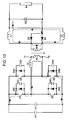
- Fig. 11 is a circuit diagram explaining an operation (mode f) in a light load mode M2 in the period (f) shown in Fig. 5 .
- Discharge of the parasitic capacitance CS4 decreases both ends voltage of the antiparallel diode DS4, and crossing the zero voltage conducts the antiparallel diode DS4.
- Conduction of the antiparallel diode DS4 inhibits flow of discharge current of the parasitic capacitance CS4 and charge current of the parasitic capacitance CS3.
- Current flowed the antiparallel diode DS4 returns to the antiparallel diode DS4 through the primary winding N1, the reactor Lr and the switching element S2. Current flowing this route increases gradually.
- Fig. 12 is a circuit diagram explaining an operation (mode g) in a light load mode M2 in the period (g) shown in Fig. 5 .
- the switching element S2 is turned-ON. Current flowing the switching element S2 becomes discharge current of the parasitic capacitance CS1 and charge current of the parasitic capacitance CS2. Charge of the parasitic capacitance CS2 increases voltage of the node T1, however, voltage of the node T2 maintains zero voltage due to conduction of the antiparallel diode D4. In this way, voltage between the node T1 and the node T2 increases in a positive direction.
- Fig. 13 is a circuit diagram explaining an operation (mode h) in a light load mode M2 in the period (h) shown in Fig. 5 .
- Discharge of the parasitic capacitance CS1 decreases both ends voltage of the antiparallel diode DS1, and crossing the zero voltage conducts the antiparallel diode DS1.
- Conduction of the antiparallel diode DS1 inhibits flow of discharge current of the parasitic capacitance CS1 and charge current of the parasitic capacitance CS2.
- Current flowed the antiparallel diode DS1 returns to the antiparallel diode DS1 through the antiparallel diode DS4, the primary winding N1 and the reactor Lr. Current flowing this route decreases gradually.
- Reason for enabling control of the output power by controlling drive frequency of the switching elements S1 and S2 is because a time period when a voltage is generated between the node T1 and the node T2 is changed. That is, by increasing the drive frequency, an effective value of the voltage between the node T1 and the node T2 per one cycle increases, and thus the output power can be increased. On the contrary, by decreasing the drive frequency, the output power also decreases.
- adoption of a switching element having a large parasitic capacitance, as the switching elements S3 and S4 is preferable because of enabling to extend the period when the voltage is generated between both ends of a transformer.
- a snubber capacitor may be connected to the switching elements S3 and S4 in parallel. It is because the addition of charge-discharge period of the snubber capacitor in the (mode a) and the (mode e) results in extending the period when the voltage is generated between the node T1 and the node T2.
- a diode having slow reverse recovery characteristics can be adopted as the antiparallel diodes DS3 and dS4.
- the voltage between the node T 1 and the node T2 is maintained till completion of reverse recovery of the antiparallel diodes DS3 and DS4. Accordingly, the output voltage can be increased.
- a switching element having fast switching characteristics may sometimes enhance efficiency.
- a MOSFET has fast switching characteristics and small switching loss.
- an enthusiast has small on-resistance and small conduction loss.
- the MOSFET is used as the switching elements S1 and S2
- the IGBT is used as the switching elements S3 and S4. In this way, switching loss in the light load mode M2 can also be decreased while suppressing conduction loss in the heavy load mode M1.
- the DC-DC converter 1 of the present invention is characterized in that, zero voltage switching becomes easy to be realized, even in the light load.
- a current required for charge-discharge of the parasitic capacitance CS1 to CS4 cannot be secured, which may sometimes provide a case that the switching elements S 1 and S2 become hard switching.
- a drive frequency of the switching elements S1 and S2 is lower as compared with a drive frequency in the heavy load mode M1. Therefore, it can be said that the present invention is effective, because even when power supply amount to the load appears nearly zero, the light load mode M2 has higher efficiency than the heavy load mode M1.
- a resonant type circuit having operation principle different from that of the phase shift type is shown.
- the frequency range should be limited for stable operation.
- many limitations in input voltage range and variation range of output voltage In addition, it requires having operation frequency apart from resonance frequency to turn down the output because the resonant circuit is a frequency controlled circuit. Therefore, it causes increase in ripple, requires bigger power to drive the elements, and thus making higher efficiency is difficult to attain.
- the operation is implemented by utilization of conduction of a diode connected to these switching elements in parallel or charge-discharge to the parasitic capacitance, in addition to ON/FF of the switching element.
- it is important how to realize zero voltage switching or switching near thereto, in performing ON/FF of the switching element. Therefore, it is important that the charge-discharge to the parasitic capacitance is controlled.
- the turn-on of the switch becomes possible by lower voltage, and switching loss decreases, as compared with a conventional control method.
- the output is more easily turned down due to low frequency, as well as because of making operation of one set of the switching elements connected in series composing one switching legs stopped, drive loss in theses switches can also be suppressed, and thus further enhancement of efficiency can be attained, as compared with a conventional control method.
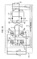
- Fig. 15 is a circuit configuration diagram of the DC-DC converter 101 according to Embodiment 2 of the present invention.
- the same reference signs will be furnished to the same parts as in Fig. 1 , and explanation thereof is omitted.
- the rectifier circuit 7 is composed of the smoothing reactor L11 and the two diodes D1 and D2. One end of the smoothing reactor L11 is connected to the diodes D1 and D2, and the other end of the smoothing reactor L11 is connected to one end of the smoothing capacitor C2. Two secondary winding N21 and N22 are connected mutually at one end thereof, and the connecting point thereof is connected to the other end of the smoothing capacitor C2.
- N21 and N22 are connected to the anode of the diode D1 and the anode of the diode D2, respectively.
- the smoothing reactor can be reduced, by which parts number can be reduced and cost can be decreased, as compared with Embodiment 1.
- the switching element instead of the diodes D1 and D2, and by using a synchronous rectifying system, further higher efficiency can be attained.
- Fig. 16 is a circuit configuration diagram of the DC-DC converter 102 according to Embodiment 3 of the present invention.
- the same reference signs will be furnished to the same parts as in Fig. 1 , and explanation thereof is omitted.
- the rectifier circuit 7 is composed of the smoothing reactor L12, the diode leg 10 connected the diodes D1 and D2 in series, and the diode leg 11 connected the diodes D3 and D4 in series and connected to the diode leg 10 in parallel.
- One end of the smoothing reactor L12 is connected to one end of the diode leg 10, the other end of the smoothing reactor L12 is connected to one end of the smoothing capacitor C2, and the other end of the diode leg 10 is connected to the other end of the smoothing capacitor C2.
- the connecting point the diodes D1 and D2, and the connecting point the diodes D3 and D4 are connected to both ends of the secondary winding N2. In this way, a diode having small peak inverse voltage can be used. Such a configuration is suitable to be used when output voltage is large.
- the switching element instead of the diodes D1 to D4, and by using a synchronous rectifying system, further higher efficiency can be attained.
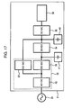
- Fig. 17 is a schematic configuration diagram of a power source system of a conventional electric vehicle 31.
- the charger 32 converts AC power from the AC power source 51 to DC power with the AC-DC converter 52, and the DC-DC converter 53 supplies a power, by transforming DC power to voltage required for charging the battery 41.
- the DC-DC converter 55 supplies power to the load 56, by transforming voltage of the battery 42, which is lower voltage than voltage of the battery 41.
- power of the battery 41 is supplied to the DC-DC converter S55 and the battery 42 by the DC-DC converter 54.
- the charger 32 had the DC-DC converter 57 to supply power from the AC-DC converter 52 to the DC-DC converter 55 and the battery 42 from the DC-DC converter 57 not via the DC-DC converter 54.
- Fig. 18 is a schematic configuration diagram of a power source system of an electric vehicle 131 adopting the DC-DC converter 1 according to Embodiment 4 of the present invention.
- the same reference code will be furnished to the same parts as in Fig. 17 , and explanation thereof is omitted.
- Adoption of the DC-DC converter 1 explained in the above Embodiment 1, instead of the DC-DC converter 54 in Fig. 17 enables for the DC-DC converter 1 to supply power in high efficiency, even in the case of small power supply amount to the load 56.
- the charger 132 requires no DC-DC converter 57 in Fig. 17 , enables to reduce parts number and to supply power in high efficiency, while attaining significant cost down.
- drive frequency of the switching elements S1 and S2 of the DC-DC converter 1 becomes lower in many cases, as compared with drive frequency in the heavy load mode M1. That is, at a time when a vehicle itself is not used such as at midnight, the battery 41 is in a charging state. In such a time, the load 56 is in a very small level minimum required. Therefore, even when power supply amount to a load is considered to be nearly zero, the light load mode M2 has higher efficiency than the heavy load mode M1, and thus it can be said that utilization of the DC-DC converter explained in the present Embodiment, for an electric vehicle is very useful.
Landscapes
- Engineering & Computer Science (AREA)
- Power Engineering (AREA)
- Dc-Dc Converters (AREA)
Priority Applications (1)
| Application Number | Priority Date | Filing Date | Title |
|---|---|---|---|
| EP19169440.5A EP3540927B1 (fr) | 2010-06-25 | 2010-06-25 | Convertisseur cc-cc |
Applications Claiming Priority (1)
| Application Number | Priority Date | Filing Date | Title |
|---|---|---|---|
| PCT/JP2010/004221 WO2011161729A1 (fr) | 2010-06-25 | 2010-06-25 | Convertisseur continu-continu |
Related Child Applications (2)
| Application Number | Title | Priority Date | Filing Date |
|---|---|---|---|
| EP19169440.5A Division EP3540927B1 (fr) | 2010-06-25 | 2010-06-25 | Convertisseur cc-cc |
| EP19169440.5A Division-Into EP3540927B1 (fr) | 2010-06-25 | 2010-06-25 | Convertisseur cc-cc |
Publications (3)
| Publication Number | Publication Date |
|---|---|
| EP2587652A1 true EP2587652A1 (fr) | 2013-05-01 |
| EP2587652A4 EP2587652A4 (fr) | 2017-11-01 |
| EP2587652B1 EP2587652B1 (fr) | 2019-06-19 |
Family
ID=45370945
Family Applications (2)
| Application Number | Title | Priority Date | Filing Date |
|---|---|---|---|
| EP19169440.5A Not-in-force EP3540927B1 (fr) | 2010-06-25 | 2010-06-25 | Convertisseur cc-cc |
| EP10853590.7A Not-in-force EP2587652B1 (fr) | 2010-06-25 | 2010-06-25 | Convertisseur continu-continu |
Family Applications Before (1)
| Application Number | Title | Priority Date | Filing Date |
|---|---|---|---|
| EP19169440.5A Not-in-force EP3540927B1 (fr) | 2010-06-25 | 2010-06-25 | Convertisseur cc-cc |
Country Status (7)
| Country | Link |
|---|---|
| US (2) | US8934265B2 (fr) |
| EP (2) | EP3540927B1 (fr) |
| JP (1) | JP5590124B2 (fr) |
| KR (1) | KR101395487B1 (fr) |
| CN (1) | CN102959846B (fr) |
| TW (1) | TWI467909B (fr) |
| WO (1) | WO2011161729A1 (fr) |
Families Citing this family (30)
| Publication number | Priority date | Publication date | Assignee | Title |
|---|---|---|---|---|
| WO2013132727A1 (fr) * | 2012-03-05 | 2013-09-12 | 富士電機株式会社 | Dispositif de conversion c.c.-c.c. |
| CN104115386A (zh) * | 2012-03-05 | 2014-10-22 | 富士电机株式会社 | 直流-直流转换装置 |
| JP5732431B2 (ja) * | 2012-05-21 | 2015-06-10 | オリジン電気株式会社 | 直列共振型コンバータシステム |
| JP5552149B2 (ja) * | 2012-10-05 | 2014-07-16 | オリジン電気株式会社 | コンバータ及び双方向コンバータ |
| JP6103874B2 (ja) * | 2012-10-12 | 2017-03-29 | 株式会社日立情報通信エンジニアリング | 電源装置とその運転方法 |
| JP6033649B2 (ja) * | 2012-11-16 | 2016-11-30 | 株式会社ダイヘン | Dc−dcコンバータ |
| TWI554015B (zh) * | 2013-04-19 | 2016-10-11 | Univ Nat Kaohsiung Applied Sci | Single - stage high power return - forward converter and light source system |
| KR101481277B1 (ko) | 2013-06-10 | 2015-01-09 | 현대자동차주식회사 | 친환경 차량의 배터리 충전용 온보드 충전기 |
| US9252672B2 (en) * | 2013-10-04 | 2016-02-02 | Chicony Power Technology Co., Ltd. | Method of controlling phase-shift full-bridge converter in light load operation |
| CN104578718B (zh) * | 2013-10-29 | 2017-10-10 | 群光电能科技股份有限公司 | 移相全桥转换器轻载控制方法 |
| KR102418750B1 (ko) * | 2014-03-17 | 2022-07-07 | 메타 시스템 - 에스.피.에이. | 전기 어플라이언스,특히 전기 자동차의 배터리 충전을 위한 배터리 충전기의 전력 공급 스테이지 |
| RU2572002C1 (ru) * | 2014-06-26 | 2015-12-27 | Борис Александрович Глебов | Способ управления преобразователем напряжения |
| JP6456063B2 (ja) * | 2014-07-14 | 2019-01-23 | 菊水電子工業株式会社 | スイッチング回路 |
| US9831790B2 (en) | 2014-09-17 | 2017-11-28 | Alps Electric Co., Ltd. | DC-to-DC converter |
| US9627979B2 (en) * | 2014-10-03 | 2017-04-18 | Bombardier Transportation Gmbh | Dual mode DC-DC converter |
| KR102344534B1 (ko) * | 2014-11-11 | 2021-12-29 | 엘지이노텍 주식회사 | 전력변환부 |
| US10158286B2 (en) * | 2015-02-02 | 2018-12-18 | Mitsubishi Electric Corporation | DC/DC converter |
| CN106067738B (zh) * | 2015-04-23 | 2020-04-14 | 松下知识产权经营株式会社 | 电力变换装置 |
| KR101703122B1 (ko) * | 2015-05-29 | 2017-02-06 | 숭실대학교산학협력단 | 배터리 진단 기능을 갖는 충전기 및 그 구동방법 |
| US9958509B2 (en) | 2015-05-29 | 2018-05-01 | Foundation Of Soongsil University-Industry Cooperation | Charger having battery diagnosis function and method of driving the same |
| US10075055B2 (en) * | 2015-09-30 | 2018-09-11 | Apple Inc. | Zero-voltage-switching scheme for phase shift converters |
| DE112017003632T5 (de) * | 2016-07-19 | 2019-04-11 | Mitsubishi Electric Corporation | Dc/dc-umrichter |
| EP3537587A4 (fr) | 2016-11-01 | 2019-11-06 | Mitsubishi Electric Corporation | Dispositif de conversion de puissance |
| EP3576281A4 (fr) * | 2017-01-30 | 2020-08-19 | Furukawa Electric Co., Ltd. | Procédé de commande d'onduleur pendant le démarrage et dispositif de commande |
| US10476398B1 (en) * | 2018-05-01 | 2019-11-12 | Postech Academy-Industry Foundation | Power conversion circuit for photovoltaic power generation with high efficiency over wide input voltage range |
| EP3853988A4 (fr) * | 2018-09-20 | 2022-04-27 | ABB Schweiz AG | Convertisseur de puissance |
| JP7105727B2 (ja) * | 2019-05-14 | 2022-07-25 | 三菱電機株式会社 | 車載用バッテリ充電装置 |
| TWI747347B (zh) * | 2020-06-30 | 2021-11-21 | 至美科技股份有限公司 | 具有半電流倍增輸出之相移全橋轉換器及其控制方法 |
| US20240258929A1 (en) * | 2021-06-04 | 2024-08-01 | Mitsubishi Electric Corporation | Power converter and power supply apparatus |
| JP7098025B1 (ja) * | 2021-06-09 | 2022-07-08 | 三菱電機株式会社 | 電力変換装置 |
Family Cites Families (18)
| Publication number | Priority date | Publication date | Assignee | Title |
|---|---|---|---|---|
| JPS6333337U (fr) | 1986-08-20 | 1988-03-03 | ||
| JP2588786B2 (ja) * | 1990-02-26 | 1997-03-12 | オリジン電気株式会社 | X線電源装置 |
| JP3318240B2 (ja) * | 1997-09-12 | 2002-08-26 | 松下電器産業株式会社 | スイッチング電源装置 |
| WO2001084699A1 (fr) * | 2000-04-28 | 2001-11-08 | Tdk Corporation | Dispositif de conversion de puissance |
| JP4466798B2 (ja) | 2000-05-26 | 2010-05-26 | サンケン電気株式会社 | 直流−直流変換器 |
| JP3482378B2 (ja) * | 2000-06-01 | 2003-12-22 | 松下電器産業株式会社 | スイッチング電源装置 |
| JP2002238257A (ja) | 2001-02-06 | 2002-08-23 | Toshiba Corp | 共振型dc−dcコンバータの制御方法 |
| JP2003047245A (ja) | 2001-07-31 | 2003-02-14 | Toshiba Corp | 電気車用電源装置 |
| JP3753978B2 (ja) | 2001-12-10 | 2006-03-08 | 株式会社東芝 | Dc−dcコンバータ制御方法 |
| JP2003324956A (ja) | 2002-05-09 | 2003-11-14 | Origin Electric Co Ltd | 直列共振型ブリッジインバータ回路の制御方法及び直列共振型ブリッジインバータ回路 |
| JP2004215469A (ja) | 2003-01-09 | 2004-07-29 | Renesas Technology Corp | スイッチング電源装置および電源制御用半導体集積回路 |
| US6856521B1 (en) * | 2003-08-19 | 2005-02-15 | General Motors Corporation | Pulse width modulation soft-switching control |
| JP2005229783A (ja) | 2004-02-16 | 2005-08-25 | Omron Corp | 燃料電池発電システム用パワーコンディショナおよびこれを用いた燃料電池発電システム |
| JP2007202370A (ja) | 2006-01-30 | 2007-08-09 | Mitsumi Electric Co Ltd | 電源装置 |
| JP4378400B2 (ja) | 2007-08-28 | 2009-12-02 | 日立コンピュータ機器株式会社 | 双方向dc−dcコンバータ及び双方向dc−dcコンバータの制御方法 |
| US7826236B2 (en) * | 2008-03-19 | 2010-11-02 | International Business Machines Corporation | Apparatus, system, and method for a switching power supply with high efficiency near zero load conditions |
| US7796405B2 (en) * | 2008-04-07 | 2010-09-14 | Dell Products, Lp | Phase shifted DC-DC converter with improved efficiency at light load |
| JP5530401B2 (ja) * | 2011-05-26 | 2014-06-25 | 株式会社日立情報通信エンジニアリング | 電源装置 |
-
2010
- 2010-06-25 EP EP19169440.5A patent/EP3540927B1/fr not_active Not-in-force
- 2010-06-25 WO PCT/JP2010/004221 patent/WO2011161729A1/fr not_active Ceased
- 2010-06-25 EP EP10853590.7A patent/EP2587652B1/fr not_active Not-in-force
- 2010-06-25 CN CN201080067480.3A patent/CN102959846B/zh not_active Expired - Fee Related
- 2010-06-25 US US13/806,819 patent/US8934265B2/en active Active
- 2010-06-25 JP JP2012521172A patent/JP5590124B2/ja not_active Expired - Fee Related
- 2010-06-25 KR KR1020127033653A patent/KR101395487B1/ko not_active Expired - Fee Related
-
2011
- 2011-05-27 TW TW100118716A patent/TWI467909B/zh not_active IP Right Cessation
-
2014
- 2014-12-08 US US14/563,693 patent/US9755524B2/en not_active Expired - Fee Related
Non-Patent Citations (1)
| Title |
|---|
| See references of WO2011161729A1 * |
Also Published As
| Publication number | Publication date |
|---|---|
| EP3540927A1 (fr) | 2019-09-18 |
| WO2011161729A1 (fr) | 2011-12-29 |
| KR101395487B1 (ko) | 2014-05-14 |
| TWI467909B (zh) | 2015-01-01 |
| EP2587652B1 (fr) | 2019-06-19 |
| US20150092452A1 (en) | 2015-04-02 |
| EP2587652A4 (fr) | 2017-11-01 |
| CN102959846B (zh) | 2015-07-15 |
| JP5590124B2 (ja) | 2014-09-17 |
| US20130100707A1 (en) | 2013-04-25 |
| US9755524B2 (en) | 2017-09-05 |
| JPWO2011161729A1 (ja) | 2013-08-19 |
| CN102959846A (zh) | 2013-03-06 |
| US8934265B2 (en) | 2015-01-13 |
| EP3540927B1 (fr) | 2020-10-14 |
| TW201223105A (en) | 2012-06-01 |
| KR20130034028A (ko) | 2013-04-04 |
Similar Documents
| Publication | Publication Date | Title |
|---|---|---|
| EP2587652B1 (fr) | Convertisseur continu-continu | |
| CN101795076B (zh) | 功率变换器以及控制功率变换器的方法 | |
| CN105144561B (zh) | Dc/dc转换器 | |
| CN101170277A (zh) | Dc-dc变换器及其控制方法 | |
| EP1742340A1 (fr) | Convertisseur dc/dc | |
| EP2523338A1 (fr) | Convertisseur alternatif-continu et procédé de commande de celui-ci | |
| JP2015159711A (ja) | スイッチング電源装置、電力変換装置 | |
| EP2757673A2 (fr) | Convertisseur | |
| US20150097507A1 (en) | Motor driving apparatus | |
| JP2015181329A (ja) | 電力変換装置 | |
| JP7100847B2 (ja) | 電力変換装置の制御装置 | |
| US7324355B2 (en) | Dc-DC converter | |
| US7196913B2 (en) | DC conversion apparatus | |
| JP2010172146A (ja) | スイッチング電源および電源制御用半導体集積回路 | |
| JP5962717B2 (ja) | Dc−dcコンバータ | |
| Khodabakhsh et al. | A comparative study of conventional and T-type ZVS-PWM full-bridge converters | |
| JP6455412B2 (ja) | プッシュプル型dc/dcコンバータ | |
| CN105048816B (zh) | Dc‑dc变换器 | |
| JP6565770B2 (ja) | プッシュプル型dc/dcコンバータ | |
| KR20100133790A (ko) | 단일단 준공진 플라이백 컨버터 | |
| JPWO2020053615A1 (ja) | 電力変換装置および電力変換装置の制御方法 | |
| JPWO2011036912A1 (ja) | 電力変換装置 | |
| KR20130083500A (ko) | 전해커패시터가 없는 단일단 배터리 충전기 |
Legal Events
| Date | Code | Title | Description |
|---|---|---|---|
| PUAI | Public reference made under article 153(3) epc to a published international application that has entered the european phase |
Free format text: ORIGINAL CODE: 0009012 |
|
| 17P | Request for examination filed |
Effective date: 20130115 |
|
| AK | Designated contracting states |
Kind code of ref document: A1 Designated state(s): AL AT BE BG CH CY CZ DE DK EE ES FI FR GB GR HR HU IE IS IT LI LT LU LV MC MK MT NL NO PL PT RO SE SI SK SM TR |
|
| DAX | Request for extension of the european patent (deleted) | ||
| RA4 | Supplementary search report drawn up and despatched (corrected) |
Effective date: 20171005 |
|
| RIC1 | Information provided on ipc code assigned before grant |
Ipc: H02M 3/335 20060101AFI20170928BHEP Ipc: H02M 1/00 20070101ALI20170928BHEP Ipc: H02M 3/28 20060101ALI20170928BHEP |
|
| GRAP | Despatch of communication of intention to grant a patent |
Free format text: ORIGINAL CODE: EPIDOSNIGR1 |
|
| STAA | Information on the status of an ep patent application or granted ep patent |
Free format text: STATUS: GRANT OF PATENT IS INTENDED |
|
| INTG | Intention to grant announced |
Effective date: 20190104 |
|
| GRAS | Grant fee paid |
Free format text: ORIGINAL CODE: EPIDOSNIGR3 |
|
| GRAA | (expected) grant |
Free format text: ORIGINAL CODE: 0009210 |
|
| STAA | Information on the status of an ep patent application or granted ep patent |
Free format text: STATUS: THE PATENT HAS BEEN GRANTED |
|
| AK | Designated contracting states |
Kind code of ref document: B1 Designated state(s): AL AT BE BG CH CY CZ DE DK EE ES FI FR GB GR HR HU IE IS IT LI LT LU LV MC MK MT NL NO PL PT RO SE SI SK SM TR |
|
| REG | Reference to a national code |
Ref country code: GB Ref legal event code: FG4D |
|
| REG | Reference to a national code |
Ref country code: CH Ref legal event code: EP |
|
| REG | Reference to a national code |
Ref country code: IE Ref legal event code: FG4D |
|
| REG | Reference to a national code |
Ref country code: DE Ref legal event code: R096 Ref document number: 602010059605 Country of ref document: DE |
|
| REG | Reference to a national code |
Ref country code: AT Ref legal event code: REF Ref document number: 1146758 Country of ref document: AT Kind code of ref document: T Effective date: 20190715 |
|
| REG | Reference to a national code |
Ref country code: NL Ref legal event code: MP Effective date: 20190619 |
|
| PG25 | Lapsed in a contracting state [announced via postgrant information from national office to epo] |
Ref country code: FI Free format text: LAPSE BECAUSE OF FAILURE TO SUBMIT A TRANSLATION OF THE DESCRIPTION OR TO PAY THE FEE WITHIN THE PRESCRIBED TIME-LIMIT Effective date: 20190619 Ref country code: SE Free format text: LAPSE BECAUSE OF FAILURE TO SUBMIT A TRANSLATION OF THE DESCRIPTION OR TO PAY THE FEE WITHIN THE PRESCRIBED TIME-LIMIT Effective date: 20190619 Ref country code: LT Free format text: LAPSE BECAUSE OF FAILURE TO SUBMIT A TRANSLATION OF THE DESCRIPTION OR TO PAY THE FEE WITHIN THE PRESCRIBED TIME-LIMIT Effective date: 20190619 Ref country code: NO Free format text: LAPSE BECAUSE OF FAILURE TO SUBMIT A TRANSLATION OF THE DESCRIPTION OR TO PAY THE FEE WITHIN THE PRESCRIBED TIME-LIMIT Effective date: 20190919 Ref country code: AL Free format text: LAPSE BECAUSE OF FAILURE TO SUBMIT A TRANSLATION OF THE DESCRIPTION OR TO PAY THE FEE WITHIN THE PRESCRIBED TIME-LIMIT Effective date: 20190619 Ref country code: HR Free format text: LAPSE BECAUSE OF FAILURE TO SUBMIT A TRANSLATION OF THE DESCRIPTION OR TO PAY THE FEE WITHIN THE PRESCRIBED TIME-LIMIT Effective date: 20190619 |
|
| REG | Reference to a national code |
Ref country code: LT Ref legal event code: MG4D |
|
| PG25 | Lapsed in a contracting state [announced via postgrant information from national office to epo] |
Ref country code: LV Free format text: LAPSE BECAUSE OF FAILURE TO SUBMIT A TRANSLATION OF THE DESCRIPTION OR TO PAY THE FEE WITHIN THE PRESCRIBED TIME-LIMIT Effective date: 20190619 Ref country code: GR Free format text: LAPSE BECAUSE OF FAILURE TO SUBMIT A TRANSLATION OF THE DESCRIPTION OR TO PAY THE FEE WITHIN THE PRESCRIBED TIME-LIMIT Effective date: 20190920 Ref country code: BG Free format text: LAPSE BECAUSE OF FAILURE TO SUBMIT A TRANSLATION OF THE DESCRIPTION OR TO PAY THE FEE WITHIN THE PRESCRIBED TIME-LIMIT Effective date: 20190919 |
|
| REG | Reference to a national code |
Ref country code: AT Ref legal event code: MK05 Ref document number: 1146758 Country of ref document: AT Kind code of ref document: T Effective date: 20190619 |
|
| PG25 | Lapsed in a contracting state [announced via postgrant information from national office to epo] |
Ref country code: NL Free format text: LAPSE BECAUSE OF FAILURE TO SUBMIT A TRANSLATION OF THE DESCRIPTION OR TO PAY THE FEE WITHIN THE PRESCRIBED TIME-LIMIT Effective date: 20190619 Ref country code: CZ Free format text: LAPSE BECAUSE OF FAILURE TO SUBMIT A TRANSLATION OF THE DESCRIPTION OR TO PAY THE FEE WITHIN THE PRESCRIBED TIME-LIMIT Effective date: 20190619 Ref country code: RO Free format text: LAPSE BECAUSE OF FAILURE TO SUBMIT A TRANSLATION OF THE DESCRIPTION OR TO PAY THE FEE WITHIN THE PRESCRIBED TIME-LIMIT Effective date: 20190619 Ref country code: EE Free format text: LAPSE BECAUSE OF FAILURE TO SUBMIT A TRANSLATION OF THE DESCRIPTION OR TO PAY THE FEE WITHIN THE PRESCRIBED TIME-LIMIT Effective date: 20190619 Ref country code: AT Free format text: LAPSE BECAUSE OF FAILURE TO SUBMIT A TRANSLATION OF THE DESCRIPTION OR TO PAY THE FEE WITHIN THE PRESCRIBED TIME-LIMIT Effective date: 20190619 Ref country code: PT Free format text: LAPSE BECAUSE OF FAILURE TO SUBMIT A TRANSLATION OF THE DESCRIPTION OR TO PAY THE FEE WITHIN THE PRESCRIBED TIME-LIMIT Effective date: 20191021 Ref country code: SK Free format text: LAPSE BECAUSE OF FAILURE TO SUBMIT A TRANSLATION OF THE DESCRIPTION OR TO PAY THE FEE WITHIN THE PRESCRIBED TIME-LIMIT Effective date: 20190619 |
|
| REG | Reference to a national code |
Ref country code: CH Ref legal event code: PL |
|
| PG25 | Lapsed in a contracting state [announced via postgrant information from national office to epo] |
Ref country code: IT Free format text: LAPSE BECAUSE OF FAILURE TO SUBMIT A TRANSLATION OF THE DESCRIPTION OR TO PAY THE FEE WITHIN THE PRESCRIBED TIME-LIMIT Effective date: 20190619 Ref country code: SM Free format text: LAPSE BECAUSE OF FAILURE TO SUBMIT A TRANSLATION OF THE DESCRIPTION OR TO PAY THE FEE WITHIN THE PRESCRIBED TIME-LIMIT Effective date: 20190619 Ref country code: IS Free format text: LAPSE BECAUSE OF FAILURE TO SUBMIT A TRANSLATION OF THE DESCRIPTION OR TO PAY THE FEE WITHIN THE PRESCRIBED TIME-LIMIT Effective date: 20191019 Ref country code: ES Free format text: LAPSE BECAUSE OF FAILURE TO SUBMIT A TRANSLATION OF THE DESCRIPTION OR TO PAY THE FEE WITHIN THE PRESCRIBED TIME-LIMIT Effective date: 20190619 |
|
| REG | Reference to a national code |
Ref country code: BE Ref legal event code: MM Effective date: 20190630 |
|
| PG25 | Lapsed in a contracting state [announced via postgrant information from national office to epo] |
Ref country code: TR Free format text: LAPSE BECAUSE OF FAILURE TO SUBMIT A TRANSLATION OF THE DESCRIPTION OR TO PAY THE FEE WITHIN THE PRESCRIBED TIME-LIMIT Effective date: 20190619 Ref country code: MC Free format text: LAPSE BECAUSE OF FAILURE TO SUBMIT A TRANSLATION OF THE DESCRIPTION OR TO PAY THE FEE WITHIN THE PRESCRIBED TIME-LIMIT Effective date: 20190619 |
|
| PG25 | Lapsed in a contracting state [announced via postgrant information from national office to epo] |
Ref country code: DK Free format text: LAPSE BECAUSE OF FAILURE TO SUBMIT A TRANSLATION OF THE DESCRIPTION OR TO PAY THE FEE WITHIN THE PRESCRIBED TIME-LIMIT Effective date: 20190619 Ref country code: IE Free format text: LAPSE BECAUSE OF NON-PAYMENT OF DUE FEES Effective date: 20190625 Ref country code: PL Free format text: LAPSE BECAUSE OF FAILURE TO SUBMIT A TRANSLATION OF THE DESCRIPTION OR TO PAY THE FEE WITHIN THE PRESCRIBED TIME-LIMIT Effective date: 20190619 |
|
| PG25 | Lapsed in a contracting state [announced via postgrant information from national office to epo] |
Ref country code: IS Free format text: LAPSE BECAUSE OF FAILURE TO SUBMIT A TRANSLATION OF THE DESCRIPTION OR TO PAY THE FEE WITHIN THE PRESCRIBED TIME-LIMIT Effective date: 20200224 Ref country code: CH Free format text: LAPSE BECAUSE OF NON-PAYMENT OF DUE FEES Effective date: 20190630 Ref country code: LI Free format text: LAPSE BECAUSE OF NON-PAYMENT OF DUE FEES Effective date: 20190630 Ref country code: LU Free format text: LAPSE BECAUSE OF NON-PAYMENT OF DUE FEES Effective date: 20190625 Ref country code: BE Free format text: LAPSE BECAUSE OF NON-PAYMENT OF DUE FEES Effective date: 20190630 |
|
| REG | Reference to a national code |
Ref country code: DE Ref legal event code: R097 Ref document number: 602010059605 Country of ref document: DE |
|
| PLBE | No opposition filed within time limit |
Free format text: ORIGINAL CODE: 0009261 |
|
| STAA | Information on the status of an ep patent application or granted ep patent |
Free format text: STATUS: NO OPPOSITION FILED WITHIN TIME LIMIT |
|
| PG2D | Information on lapse in contracting state deleted |
Ref country code: IS |
|
| PG25 | Lapsed in a contracting state [announced via postgrant information from national office to epo] |
Ref country code: FR Free format text: LAPSE BECAUSE OF NON-PAYMENT OF DUE FEES Effective date: 20190819 |
|
| 26N | No opposition filed |
Effective date: 20200603 |
|
| PG25 | Lapsed in a contracting state [announced via postgrant information from national office to epo] |
Ref country code: SI Free format text: LAPSE BECAUSE OF FAILURE TO SUBMIT A TRANSLATION OF THE DESCRIPTION OR TO PAY THE FEE WITHIN THE PRESCRIBED TIME-LIMIT Effective date: 20190619 |
|
| GBPC | Gb: european patent ceased through non-payment of renewal fee |
Effective date: 20190919 |
|
| PG25 | Lapsed in a contracting state [announced via postgrant information from national office to epo] |
Ref country code: GB Free format text: LAPSE BECAUSE OF NON-PAYMENT OF DUE FEES Effective date: 20190919 |
|
| PG25 | Lapsed in a contracting state [announced via postgrant information from national office to epo] |
Ref country code: CY Free format text: LAPSE BECAUSE OF FAILURE TO SUBMIT A TRANSLATION OF THE DESCRIPTION OR TO PAY THE FEE WITHIN THE PRESCRIBED TIME-LIMIT Effective date: 20190619 |
|
| PG25 | Lapsed in a contracting state [announced via postgrant information from national office to epo] |
Ref country code: HU Free format text: LAPSE BECAUSE OF FAILURE TO SUBMIT A TRANSLATION OF THE DESCRIPTION OR TO PAY THE FEE WITHIN THE PRESCRIBED TIME-LIMIT; INVALID AB INITIO Effective date: 20100625 Ref country code: MT Free format text: LAPSE BECAUSE OF FAILURE TO SUBMIT A TRANSLATION OF THE DESCRIPTION OR TO PAY THE FEE WITHIN THE PRESCRIBED TIME-LIMIT Effective date: 20190619 |
|
| PG25 | Lapsed in a contracting state [announced via postgrant information from national office to epo] |
Ref country code: MK Free format text: LAPSE BECAUSE OF FAILURE TO SUBMIT A TRANSLATION OF THE DESCRIPTION OR TO PAY THE FEE WITHIN THE PRESCRIBED TIME-LIMIT Effective date: 20190619 |
|
| PGFP | Annual fee paid to national office [announced via postgrant information from national office to epo] |
Ref country code: DE Payment date: 20230502 Year of fee payment: 14 |
|
| REG | Reference to a national code |
Ref country code: DE Ref legal event code: R119 Ref document number: 602010059605 Country of ref document: DE |
|
| PG25 | Lapsed in a contracting state [announced via postgrant information from national office to epo] |
Ref country code: DE Free format text: LAPSE BECAUSE OF NON-PAYMENT OF DUE FEES Effective date: 20250101 |