EP2587903A2 - Boîtier et dispositif électronique lýutilisant - Google Patents
Boîtier et dispositif électronique lýutilisant Download PDFInfo
- Publication number
- EP2587903A2 EP2587903A2 EP12165416.4A EP12165416A EP2587903A2 EP 2587903 A2 EP2587903 A2 EP 2587903A2 EP 12165416 A EP12165416 A EP 12165416A EP 2587903 A2 EP2587903 A2 EP 2587903A2
- Authority
- EP
- European Patent Office
- Prior art keywords
- housing
- main body
- electronic device
- top surface
- protrusions
- Prior art date
- Legal status (The legal status is an assumption and is not a legal conclusion. Google has not performed a legal analysis and makes no representation as to the accuracy of the status listed.)
- Withdrawn
Links
- 239000010410 layer Substances 0.000 claims 2
- 239000011241 protective layer Substances 0.000 claims 2
- 230000000007 visual effect Effects 0.000 abstract description 4
- 238000000034 method Methods 0.000 description 5
- 239000000919 ceramic Substances 0.000 description 1
- 238000003486 chemical etching Methods 0.000 description 1
- 239000011521 glass Substances 0.000 description 1
- 230000001788 irregular Effects 0.000 description 1
- 238000010147 laser engraving Methods 0.000 description 1
- 239000000463 material Substances 0.000 description 1
- 230000003647 oxidation Effects 0.000 description 1
- 238000007254 oxidation reaction Methods 0.000 description 1
- 239000003973 paint Substances 0.000 description 1
- 239000004033 plastic Substances 0.000 description 1
- 238000002310 reflectometry Methods 0.000 description 1
- 238000004381 surface treatment Methods 0.000 description 1
Images


Classifications
-
- H—ELECTRICITY
- H05—ELECTRIC TECHNIQUES NOT OTHERWISE PROVIDED FOR
- H05K—PRINTED CIRCUITS; CASINGS OR CONSTRUCTIONAL DETAILS OF ELECTRIC APPARATUS; MANUFACTURE OF ASSEMBLAGES OF ELECTRICAL COMPONENTS
- H05K5/00—Casings, cabinets or drawers for electric apparatus
- H05K5/02—Details
- H05K5/0217—Mechanical details of casings
- H05K5/0243—Mechanical details of casings for decorative purposes
-
- H—ELECTRICITY
- H04—ELECTRIC COMMUNICATION TECHNIQUE
- H04M—TELEPHONIC COMMUNICATION
- H04M1/00—Substation equipment, e.g. for use by subscribers
- H04M1/02—Constructional features of telephone sets
- H04M1/0202—Portable telephone sets, e.g. cordless phones, mobile phones or bar type handsets
- H04M1/0279—Improving the user comfort or ergonomics
- H04M1/0283—Improving the user comfort or ergonomics for providing a decorative aspect, e.g. customization of casings, exchangeable faceplate
Definitions
- the disclosure relates to a housing and an electronic device employing the housing.
- the surface treatment method may be a laser engraving process, an anodic oxidation process, or a chemical etching process. However, these methods are not always so successful at forming novel and attractive patterns.
- a housing for an electronic device includes a main body and a plurality of prismatic-shaped protrusions formed on a surface of the main body. Each protrusion has a top surface slanted relative to the main body.
- an electronic device using a housing includes a main body and a plurality of prismatic-shaped protrusions formed on a surface of the main body. Each protrusion has a top surface slanted relative to the main body.
- FIG. 1 is a schematic view of a first exemplary embodiment of a housing.
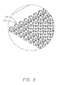
- FIG. 2 is a partial enlarged view of FIG. 1 .
- FIG. 3 is a schematic view of a second exemplary embodiment of a housing.
- FIG. 1 shows a housing 100 according to a first exemplary embodiment.
- the housing 100 is made of plastic, glass, or ceramic.
- the housing 100 includes a plate-shaped main body 110 and a plurality of equally spaced apart prismatic-shaped protrusions 130 defined on a surface of the main body 110.
- FIG. 2 shows an enlarged view of the housing 100.
- Each protrusion 130 has a top surface 131.
- Each top surface 131 is a quadrilateral surface slanted relative to the main body 110. The directions and angles of the slanting relative to the main body can be set as needed to create different visual effects. Observing from the side of the housing 100, the top surfaces 131 present different visual effects of light and shade due to setting the top surfaces 131 at different angles, which makes the protrusions 130 present a desired pattern.
- FIG. 3 shows a housing 200 according to a second exemplary embodiment.
- the housing 200 includes a plate-shaped main body 210 and a plurality of prismatic-shaped protrusions 230 formed on a surface of the main body 210. Where in the first embodiment adjacent protrusions 130 are spaced apart, in this second embodiment, adjacent protrusions 230 are not spaced apart and are in contact with each other.
- Each protrusion 230 also has a top surface 231 which is an irregular polygon surface slanted relative to the main body 210. As in the previous embodiment, directions and angles of the slanting can be set as needed to create different visual effects.
- top surfaces 131 and 231 of the protrusions 130 and 230 can also be other shapes, such as elliptical, triangular, or other polygonal shapes.
- top surfaces 131 and 231 of the protrusions 130 and 230 may be coated with a layer of paint or other materials to enhance reflectivity or to protect the housings 100 and 200.
- the housings 100 and 200 can be used as shells of electronic devices.
Landscapes
- Engineering & Computer Science (AREA)
- Signal Processing (AREA)
- Microelectronics & Electronic Packaging (AREA)
- Casings For Electric Apparatus (AREA)
Applications Claiming Priority (1)
| Application Number | Priority Date | Filing Date | Title |
|---|---|---|---|
| CN2011103256251A CN103068192A (zh) | 2011-10-24 | 2011-10-24 | 壳体 |
Publications (2)
| Publication Number | Publication Date |
|---|---|
| EP2587903A2 true EP2587903A2 (fr) | 2013-05-01 |
| EP2587903A3 EP2587903A3 (fr) | 2015-07-01 |
Family
ID=46049219
Family Applications (1)
| Application Number | Title | Priority Date | Filing Date |
|---|---|---|---|
| EP12165416.4A Withdrawn EP2587903A3 (fr) | 2011-10-24 | 2012-04-24 | Boîtier et dispositif électronique l'utilisant |
Country Status (3)
| Country | Link |
|---|---|
| US (1) | US20130100592A1 (fr) |
| EP (1) | EP2587903A3 (fr) |
| CN (1) | CN103068192A (fr) |
Families Citing this family (9)
| Publication number | Priority date | Publication date | Assignee | Title |
|---|---|---|---|---|
| CN104754888A (zh) * | 2013-12-25 | 2015-07-01 | 正达国际光电股份有限公司 | 玻璃外壳、制造该玻璃外壳的成型模具及成型方法 |
| US20180320859A1 (en) * | 2017-05-04 | 2018-11-08 | Case-Mate, Inc. | Electronics case with light-reflective elements |
| CN108873117B (zh) * | 2017-05-16 | 2020-04-21 | 昇印光电(昆山)股份有限公司 | 光学元件、手机盖板及制备光学元件的模具 |
| CN108873118B (zh) | 2017-05-16 | 2020-06-26 | 昇印光电(昆山)股份有限公司 | 光学元件、手机盖板及用于制备该光学元件的模具 |
| CN107770314B (zh) * | 2017-11-29 | 2020-03-24 | Oppo广东移动通信有限公司 | 移动终端保护壳和移动终端 |
| WO2019105268A1 (fr) * | 2017-11-29 | 2019-06-06 | Oppo广东移动通信有限公司 | Étui de protection pour dispositif électronique, et dispositif électronique |
| USD880469S1 (en) | 2019-01-24 | 2020-04-07 | Spigen Korea Co., Ltd. | Case for electronic communications device |
| CN114615838B (zh) * | 2020-12-09 | 2023-03-21 | Oppo广东移动通信有限公司 | 壳体组件及其制备方法和电子设备 |
| CN116867205A (zh) * | 2021-09-30 | 2023-10-10 | Oppo广东移动通信有限公司 | 壳体及电子设备 |
Family Cites Families (7)
| Publication number | Priority date | Publication date | Assignee | Title |
|---|---|---|---|---|
| JP4584003B2 (ja) * | 2005-04-07 | 2010-11-17 | セイコーエプソン株式会社 | ラベル作成装置のラベル作成方法、およびラベル作成装置 |
| CN101325620A (zh) * | 2007-06-14 | 2008-12-17 | 鸿富锦精密工业(深圳)有限公司 | 防辐射手机壳体 |
| CN101420829B (zh) * | 2007-10-25 | 2011-09-21 | 深圳富泰宏精密工业有限公司 | 金属外壳及其制作方法 |
| US7667956B2 (en) * | 2008-04-09 | 2010-02-23 | High Tech Computer Corporation | Portable electronic apparatus and housing thereof |
| CN101730410A (zh) * | 2008-10-20 | 2010-06-09 | 深圳富泰宏精密工业有限公司 | 外壳及其制造方法 |
| CN102049957A (zh) * | 2009-10-29 | 2011-05-11 | 深圳富泰宏精密工业有限公司 | 陶瓷塑料复合制品及其制作方法 |
| CN102770787B (zh) * | 2009-12-01 | 2015-09-16 | 凸版印刷株式会社 | 显示体及带标签的物品 |
-
2011
- 2011-10-24 CN CN2011103256251A patent/CN103068192A/zh active Pending
-
2012
- 2012-04-06 US US13/441,297 patent/US20130100592A1/en not_active Abandoned
- 2012-04-24 EP EP12165416.4A patent/EP2587903A3/fr not_active Withdrawn
Non-Patent Citations (1)
| Title |
|---|
| None |
Also Published As
| Publication number | Publication date |
|---|---|
| US20130100592A1 (en) | 2013-04-25 |
| EP2587903A3 (fr) | 2015-07-01 |
| CN103068192A (zh) | 2013-04-24 |
Similar Documents
| Publication | Publication Date | Title |
|---|---|---|
| EP2587903A2 (fr) | Boîtier et dispositif électronique lýutilisant | |
| KR101914298B1 (ko) | 디스플레이용 글라스 윈도우 가공 장치 및 방법 | |
| US10562273B2 (en) | Cover glass lamination structure and manufacturing method thereof | |
| US10526237B2 (en) | Cover glass lamination structure and manufacturing method thereof | |
| US20140078412A1 (en) | Exposed Glass Article with Inner Recessed Area for Portable Electronic Device Housing | |
| EP4258847A3 (fr) | Appareil d'affichage | |
| EP3552134A4 (fr) | Procédé d'authentification adaptative et dispositif électronique le supportant | |
| EP3220433A3 (fr) | Afficheur | |
| CN104981124B (zh) | 移动终端及其壳体及壳体的加工方法 | |
| EP3196735A3 (fr) | Dispositif tactile, afficheur le comprenant et son procédé de fabrication | |
| EP2777909A3 (fr) | Boîtier, procédé de fabrication de boîtier et dispositif électronique | |
| EP4394486A3 (fr) | Procédé de réseau incliné à hauteur variable | |
| EP2025466A3 (fr) | Appareil de polissage, procédé de fabrication de substrat, et procédé de fabrication d'un appareil électronique | |
| EP2495643A3 (fr) | Procédé de fabrication de substrat de circuit transparent pour écran tactile | |
| CN107799009A (zh) | 覆盖窗、包括覆盖窗的显示装置及制造覆盖窗的方法 | |
| EP2913420A3 (fr) | Procédés de revêtement et substrat revêtu | |
| WO2011071753A3 (fr) | Génération de motifs combinatoires par inclinaison délibérée d'un réseau de plumes polymère | |
| EP2302989A3 (fr) | Appareil support de substrat | |
| MY176154A (en) | Body having fine concave portions and convex portions in surface, and production method of body having fine concave portions and convex portions in surface | |
| TW201716954A (zh) | 具隱藏式盲孔之顯示面板結構及其製作方法 | |
| US20190045643A1 (en) | Anti-Slip Substrates | |
| US20160185067A1 (en) | Housing, electronic device using same, and method for making same | |
| ATE393839T1 (de) | Verfahren zur gehäusebildung bei elektronischen bauteilen so wie so hermetisch verkapselte elektronische bauteile | |
| EP2770310A3 (fr) | Filtre d'interférence de longueur d'onde variable, filtre optique, module optique et appareil électronique | |
| DE60134997D1 (de) | Hydrophile oberfläche mit temporären schutzverkleidungen |
Legal Events
| Date | Code | Title | Description |
|---|---|---|---|
| PUAI | Public reference made under article 153(3) epc to a published international application that has entered the european phase |
Free format text: ORIGINAL CODE: 0009012 |
|
| AK | Designated contracting states |
Kind code of ref document: A2 Designated state(s): AL AT BE BG CH CY CZ DE DK EE ES FI FR GB GR HR HU IE IS IT LI LT LU LV MC MK MT NL NO PL PT RO RS SE SI SK SM TR |
|
| AX | Request for extension of the european patent |
Extension state: BA ME |
|
| PUAL | Search report despatched |
Free format text: ORIGINAL CODE: 0009013 |
|
| AK | Designated contracting states |
Kind code of ref document: A3 Designated state(s): AL AT BE BG CH CY CZ DE DK EE ES FI FR GB GR HR HU IE IS IT LI LT LU LV MC MK MT NL NO PL PT RO RS SE SI SK SM TR |
|
| AX | Request for extension of the european patent |
Extension state: BA ME |
|
| RIC1 | Information provided on ipc code assigned before grant |
Ipc: H05K 5/02 20060101AFI20150528BHEP Ipc: H04M 1/02 20060101ALI20150528BHEP |
|
| STAA | Information on the status of an ep patent application or granted ep patent |
Free format text: STATUS: THE APPLICATION IS DEEMED TO BE WITHDRAWN |
|
| 18D | Application deemed to be withdrawn |
Effective date: 20151103 |