EP2589055B1 - Transformator für galvanische trennung - Google Patents
Transformator für galvanische trennung Download PDFInfo
- Publication number
- EP2589055B1 EP2589055B1 EP11810082.5A EP11810082A EP2589055B1 EP 2589055 B1 EP2589055 B1 EP 2589055B1 EP 11810082 A EP11810082 A EP 11810082A EP 2589055 B1 EP2589055 B1 EP 2589055B1
- Authority
- EP
- European Patent Office
- Prior art keywords
- integrated circuit
- transformer
- die
- quartz substrate
- voltage
- Prior art date
- Legal status (The legal status is an assumption and is not a legal conclusion. Google has not performed a legal analysis and makes no representation as to the accuracy of the status listed.)
- Active
Links
Images

Classifications
-
- H—ELECTRICITY
- H10—SEMICONDUCTOR DEVICES; ELECTRIC SOLID-STATE DEVICES NOT OTHERWISE PROVIDED FOR
- H10W—GENERIC PACKAGES, INTERCONNECTIONS, CONNECTORS OR OTHER CONSTRUCTIONAL DETAILS OF DEVICES COVERED BY CLASS H10
- H10W44/00—Electrical arrangements for controlling or matching impedance
- H10W44/501—Inductive arrangements
-
- H—ELECTRICITY
- H10—SEMICONDUCTOR DEVICES; ELECTRIC SOLID-STATE DEVICES NOT OTHERWISE PROVIDED FOR
- H10W—GENERIC PACKAGES, INTERCONNECTIONS, CONNECTORS OR OTHER CONSTRUCTIONAL DETAILS OF DEVICES COVERED BY CLASS H10
- H10W90/00—Package configurations
-
- H—ELECTRICITY
- H01—ELECTRIC ELEMENTS
- H01F—MAGNETS; INDUCTANCES; TRANSFORMERS; SELECTION OF MATERIALS FOR THEIR MAGNETIC PROPERTIES
- H01F19/00—Fixed transformers or mutual inductances of the signal type
- H01F19/04—Transformers or mutual inductances suitable for handling frequencies considerably beyond the audio range
- H01F19/08—Transformers having magnetic bias, e.g. for handling pulses
- H01F2019/085—Transformer for galvanic isolation
-
- Y—GENERAL TAGGING OF NEW TECHNOLOGICAL DEVELOPMENTS; GENERAL TAGGING OF CROSS-SECTIONAL TECHNOLOGIES SPANNING OVER SEVERAL SECTIONS OF THE IPC; TECHNICAL SUBJECTS COVERED BY FORMER USPC CROSS-REFERENCE ART COLLECTIONS [XRACs] AND DIGESTS
- Y10—TECHNICAL SUBJECTS COVERED BY FORMER USPC
- Y10T—TECHNICAL SUBJECTS COVERED BY FORMER US CLASSIFICATION
- Y10T29/00—Metal working
- Y10T29/49—Method of mechanical manufacture
- Y10T29/49002—Electrical device making
- Y10T29/49117—Conductor or circuit manufacturing
- Y10T29/49124—On flat or curved insulated base, e.g., printed circuit, etc.
- Y10T29/49128—Assembling formed circuit to base
Definitions
- the present invention relates to galvanic isolation in an electrical system and, in particular, to formation of a galvanic isolation transformer on a quartz substrate.
- Galvanic isolation for integrated circuits requires a device that electrically isolates two systems to a high target isolation voltage, e.g. 5kV, but that transmits data between systems that are at different ground potentials.
- a high target isolation voltage e.g. 5kV
- One solution is a multi-die approach that utilizes a transformer between the die that are to be isolated from each other; short pulses generated on one die system are transmitted across the transformer to be decoded by the second die system.
- Another solution is similar to that just described, but uses a capacitor to isolate the two die systems instead of a transformer.
- Yet another solution utilizes optical coupling, whereby a light emitting diode (LED) on one die system emits light and a photodiode on the second die system detects the light and generates corresponding electrical current.
- LED light emitting diode
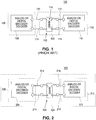
- Fig. 1 shows a multi-die galvanic isolation design 100 that utilizes a transformer 102 formed on a single silicon substrate 104 to create galvanic isolation between a first integrated circuit 106 formed on a first silicon die 108 and a second integrated circuit 110 formed on a second silicon die 112.
- Fig. 1 shows the transformer 102 connected between the first integrated circuit 106 and the second integrated circuit 110 by wire bonds 114 that electrically connect the first silicon die 108 and the second silicon die 112 to the "transformer" substrate 104.
- the dielectric 116 (shown schematically in Fig. 1 ) formed between the windings of the transformer 102 must be thick enough to hold off the voltage difference between the first integrated circuit 106 and the second integrated circuit 110.
- an analog or digital encoder/decoder included in the first integrated circuit 106 takes data generated by the first integrated circuit 106, encodes it and transmits it across the transformer 102.
- There are a number of existing methods used to transfer voltage or current across a transformer e.g., very short, square pulses or via a high frequency rf carrier sinusoidal wave.
- An analog or digital encoder/decoder included in the second integrated circuit 110 detects the transmitted encoded data, decodes them and extracts the data for utilization by the second integrated circuit 110.
- inter-wound planar type utilizes a single metal layer and the windings are separated based upon layout design.
- stacked type utilizes two layers of metal that are separated by a distance that is great enough to hold off the voltage difference in the two windings.
- At least four types of isolation are required: winding-to-winding isolation, winding-to-substrate isolation, bond wire-to-bond wire isolation and die-to-die isolation.
- the minimum distance for winding-to-winding isolation is determined from the dielectric strength of the insulator used between the windings. Table 1 below provides an overview of several dielectric materials commonly utilized in the semiconductor processing and packaging industry and the distance required for isolation of 5kV. Typically, the distances utilized in an actual device are greater to safely account for differences in dielectric quality and uniformity.
- the minimum distance for winding-to-substrate isolation is determined differently for a stacked transformer and an inter-wound transformer.
- the high voltage side is in the top metal layer which, by design, is located a sufficient distance from the substrate to avoid dielectric breakdown to the substrate.
- the metal layer i.e. both windings of the transformer, must be sufficiently distanced from the silicon substrate so that dielectric breakdown does not occur at the isolation voltage. The distance is similar to the distances shown in Table 1 and depends upon the material stack between the metal layers and the substrate.
- the bond wire-to-bond wire spacing is dictated by the molding compound with which the final package is injected.
- a typical compound might be the Sumitomo G700 series of molding compounds that has a listed dielectric strength of 15 V/ ⁇ m.
- the spacing between bond pads and wires must be sufficiently large that breakdown will never occur in the molding compound.
- the molding compound is the least well controlled of all materials within the package and, therefore, would introduce too much variation.
- the die-to-die breakdown voltage is similarly defined through the molding compound.
- integrated circuits are built on silicon substrates on copper leadframes, which means that two silicon die cannot be mounted on the same die attach pad (DAP). This forces the use of two DAP leadframes with a space in between which is subsequently filled with molding compound. Similarly to the wire bonds, the distance between the two DAPs must be sufficient to exceed the rated dielectric withstand voltage.
- US 7,064,442 relates to an integrated circuit package device.
- US 2008/0278275 relates to miniature transformers adapted for use in galvanic isolators and the like.
- US 2001/0050607 relates to an integrated transformer.
- an integrated circuit system comprises a quartz substrate, a first integrated circuit die system attached to the substrate and having a first voltage associated therewith, a second integrated circuit die system attached to the substrate and having a second voltage associated therewith, the second voltage being less than the first voltage, and a transformer formed on the substrate and electrically connected between the first integrated circuit die system and the second integrated circuit die system to provide galvanic isolation therebetween.
- a method of forming an integrated circuit system comprises providing a first integrated circuit die having a first integrated circuit formed thereon, providing a second integrated circuit die having a second integrated circuit formed thereon, and electrically connecting a transformer formed on a quartz substrate between the first integrated circuit and the second integrated circuit to provide galvanic isolation therebetween, wherein the first integrated circuit die and the second integrated circuit die are attached to the quartz substrate.
- a galvanic isolation transformer may be created in one or more layers of metal, but above a quartz wafer rather than a silicon wafer. Quartz, similar to silicon dioxide, is a dielectric isolator, which therefore means that the breakdown from the high voltage winding of the transformer to the substrate is removed.
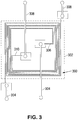
- Fig. 2 shows an integrated circuit system 200 that includes a transformer 202 formed on a quartz substrate 204 and connected between a first integrated circuit 206 formed on a first semiconductor (e.g., silicon) die 208 and a second integrated circuit 210 formed on a second semiconductor (e.g., silicon) die 212. According to the embodiments, both the first semiconductor die 208 and the second semiconductor die 212 are also formed on the quartz substrate 204.
- the first integrated circuit 206 has a first voltage, e.g., greater than or equal to 5kV, associated therewith and the second integrated circuit 210 has a second voltage associated therewith that is less than the first voltage.
- Fig. 2 shows an integrated circuit system 200 that includes a transformer 202 formed on a quartz substrate 204 and connected between a first integrated circuit 206 formed on a first semiconductor (e.g., silicon) die 208 and a second integrated circuit 210 formed on a second semiconductor (e.g., silicon) die 212. According to the embodiments, both the first semiconductor die
- FIG. 2 shows wire bonds 214 that electrically connect the transformer 202 between the first integrated circuit 206 and the second integrated circuit 210.
- an analog or digital encoder/decoder included in the first integrated circuit 206 takes data generated by the first integrated circuit 206, encodes it and transmits it across transformer 102 utilizing either very short, square pulses or a high frequency carrier; an analog or digital encoder/decoder included in the second integrated circuit 210 detects the pulses, decodes them and extracts the data for utilization by the second integrated circuit 210.
- the integrated circuit system design shown in Fig. 2 could be implemented using two die attach paddles (DAPs) inside a package.
- the DAP would then act as the support for the die.
- the Fig. 2 design shows the system formed entirely on a single quartz substrate 204.
- the first silicon die 208 and the second silicon die 212 are attached to the quartz substrate 204 using bond adhesive.
- Bonding adhesive well known to those skilled in the art can be used to bond quartz to silicon or to a metal plate, e.g. using Cu, can be patterned and the bond is then between the metal plate and the silicon, which is a more standard approach.
- the advantages to forming the integrated circuit system entirely on the quartz substrate include, but are not limited to: isolation between the three circuits is achieved; a single DAP inside the package can be utilized, thereby simplifying package design; the DAP can be either conductive or non-conductive, whichever is the lowest cost; the ability to use local routing of copper interconnect on quartz, thereby allowing optimal placement of bond pads for wire bonding from the DAP to the leadframe; tighter packaging of die compared with using multiple DAPs inside a package; the two silicon die can also be bumped (pads are metal bumps), flip-chipped and bonded to copper pads defined on the surface of the quartz substrate, thereby reducing the number of wire bonds and reducing parasitic associated therewith.
- the transformer 202 may be either an inter-wound type that utilizes a single metal layer and windings that are separated by dielectric material based upon layout design or a stacked type that utilizes two layers of metal that are separated by dielectric material by a distance that is great enough to hold off the voltage difference between the two windings.
- the dielectric material may be selected from (but not limited to) the dielectric material identified in Table 1 above.
- the transformers described herein are air core transformers; however, those skilled in the art will appreciate that the concepts disclosed herein are also applicable to transformers with magnetic cores.
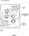
- Fig. 3 shows an inter-wound transformer 300 formed on a quartz substrate 302.
- Wire bonds 304 provide electrical connection between a high voltage integrated circuit (e.g., having a voltage equal to or greater than 5kV associated therewith) formed on a first semiconductor die and a copper high voltage winding 306 of the inter-wound transformer 300.
- Wire bonds 308 provide electrical connection between a "low" voltage integrated circuit formed on a second semiconductor die and the copper low voltage winding 310 of the inter-wound transformer 300.
- the copper high voltage winding 306 and the copper low voltage winding 310 are separated by a dielectric, e.g., benzocyclobutene (BCB), having a minimum winding separation thickness that is based upon layout design.
- BCB benzocyclobutene
- the copper metal width of the transformer windings may be 20 ⁇ m, the spacing between windings may be 25 ⁇ m and the thickness of the windings may be 5 ⁇ m in a transformer having 7/7 turns (not shown in the Fig. 3 schematic drawing), an outer size of 2100x2100 ⁇ m and an inner size of 800x800 ⁇ m.
- Fig. 4 shows a cross section of the Fig. 3 inter-wound transformer 300 with a BCB layer 10 ⁇ m thick separating turns of the copper high voltage winding 306 and the turns of copper low voltage winding 310.
- the processing aspects of the inter-wound planar transformer embodiment 300 shown in Figs. 3 and 4 are advantageous since the copper high voltage winding 304 and the copper low voltage winding may be either plated or deposited directly onto the quartz substrate 302 in accordance with techniques well known to those skilled in the art. Copper adhesion to quartz is very good, as are the stress and wafer bow. As stated above, no dielectric breakdown to the substrate 302 will occur because quartz is an insulator. The dielectric strength of quartz is 25-40 V/ ⁇ m, which with a 750 ⁇ m (or greater) thick quartz substrate means that there will be no premature breakdown to the substrate. Before the quartz can be packaged, the wafer is thinned down, e.g. to 16 mils, and care should be taken to ensure that the breakdown voltage to the substrate is maintained above the rated isolation rating.
- Fig. 5 shows the frequency response of the inter-wound transformer 300 on quartz shown in Figs. 3 and 4 .
- the metal is 5 ⁇ m thick copper, there are 7 windings to the spiral, the metal width is 20 ⁇ m and the metal-metal spacing is 25 ⁇ m.
- the metal is covered by a 10 ⁇ m thick layer of BCB as a passivation layer.
- the quartz substrate achieves maximum Q at a frequency of 400MHz compared with the same design on a silicon wafer which achieves a frequency of 70MHz.
- the maximum Q of the quartz substrate is also much higher: 19 in Fig. 5 compared with 10 for the silicon wafer.
- Fig. 6 shows a multi-channel embodiment wherein a high voltage silicon die and a low voltage silicon die, together with four inter-wound transformers, are bonded to a quartz substrate.
- the transformers are shown in Fig. 6 as an inter-wound octaganal design, other inter-woven designs (e.g. the design shown in Figs. 3 and 4 )or stacked designs may be utilized.
- Local routing of copper on quartz is utilized to interconnect the four inter-wound transformers between the high voltage die and the low voltage die.
- the four transformers may be integrated into a 44 Lead PLCC package. This allows the metal pads for the bond wires to be distributed around the edges of the quartz substrate and connected to the transformers using local copper interconnect. Without the use of a common quartz substrate and the local routing of copper interconnected on quartz to distribute wire bond pads, this multi-channel design could not fit into the 44 Lead PLCC package.
Landscapes
- Semiconductor Integrated Circuits (AREA)
- Coils Or Transformers For Communication (AREA)
Claims (10)
- Integriertes Schaltungssystem, das Folgendes umfasst:ein Quarzsubstrat (204);einen ersten integrierten Schaltungschip (208), der am Quarzsubstrat (204) angebracht ist und eine erste integrierte Schaltung (206) besitzt, die auf ihm gebildet ist, wobei der ersten integrierten Schaltung (206) eine erste Spannung zugeordnet ist;einen zweiten integrierten Schaltungschip (212), der am Quarzsubstrat (204) angebracht ist und eine zweite integrierte Schaltung (210) besitzt, die auf ihm gebildet ist, wobei der zweiten integrierten Schaltung (210) eine zweite Spannung zugeordnet ist und die zweite Spannung kleiner als die erste Spannung ist; undein Transformatorsystem (202), das auf dem Quarzsubstrat (204) gebildet ist und zwischen der ersten integrierten Schaltung (206) und der zweiten integrierten Schaltung (210) elektrisch verbunden ist, um dazwischen eine galvanische Isolation bereitzustellen.
- Integriertes Schaltungssystem nach Anspruch 1, wobei die erste Spannung größer oder gleich 5 kV ist.
- Integriertes Schaltungssystem nach Anspruch 1, wobei das Transformatorsystem (202) einen übergreifend gewickelten Transformator umfasst.
- Integriertes Schaltungssystem nach Anspruch 1, wobei das Transformatorsystem (202) einen gestapelten Transformator umfasst.
- Integriertes Schaltungssystem nach Anspruch 1, wobei das Transformatorsystem (202) mehrere übergreifend gewickelte Transformatoren umfasst, um eine Mehrkanalsignalkommunikation zwischen der ersten integrierten Schaltung (206) und der zweiten integrierten Schaltung (210) bereitzustellen.
- Integriertes Schaltungssystem nach Anspruch 1, wobei
die erste integrierte Schaltung (206) einen ersten Codierer/Decodierer enthält, der Daten codiert, die durch die erste integrierte Schaltung (206) erzeugt werden, und mittels des Transformatorsystems (202) die codierten Daten zur zweiten integrierten Schaltung (210) sendet, und
die zweite integrierte Schaltung (210) einen zweiten Codierer/Decodierer enthält, der die codierten Daten, die durch die erste integrierte Schaltung (206) gesendet wurden, decodiert und die Daten zur Verwendung durch die zweite integrierte Schaltung (210) extrahiert. - Verfahren zum Bilden eines integrierten Schaltungssystems, das Folgendes umfasst:Bereitstellen eines ersten integrierten Schaltungschip (208), der eine erste integrierte Schaltung (206) besitzt, die auf ihm gebildet ist;Bereitstellen eines zweiten integrierten Schaltungschip (212), der eine zweite integrierte Schaltung (210) besitzt, die auf ihm gebildet ist; undelektrisches Verbinden eines Transformatorsystems (202), das auf dem Quarzsubstrat (204) gebildet ist, zwischen der ersten integrierten Schaltung (206) und der zweiten integrierten Schaltung (210), um eine galvanische Isolation dazwischen bereitzustellen, wobei der erste integrierte Schaltungschip (208) und der zweite integrierte Schaltungschip (212) am Quarzsubstrat (204) angebracht sind.
- Verfahren nach Anspruch 7, wobei das Transformatorsystem (202) einen übergreifend gewickelten Transformator umfasst.
- Verfahren nach Anspruch 7, wobei das Transformatorsystem (202) einen gestapelten Transformator umfasst.
- Verfahren nach Anspruch 7, wobei das Transformatorsystem (202) mehrere übergreifend gewickelte Transformatoren umfasst, um eine Mehrkanalsignalkommunikation zwischen der ersten integrierten Schaltung (206) und der zweiten integrierten Schaltung (210) bereitzustellen.
Applications Claiming Priority (2)
| Application Number | Priority Date | Filing Date | Title |
|---|---|---|---|
| US12/827,316 US20120002377A1 (en) | 2010-06-30 | 2010-06-30 | Galvanic isolation transformer |
| PCT/US2011/041951 WO2012012108A2 (en) | 2010-06-30 | 2011-06-27 | Galvanic isolation transformer |
Publications (3)
| Publication Number | Publication Date |
|---|---|
| EP2589055A2 EP2589055A2 (de) | 2013-05-08 |
| EP2589055A4 EP2589055A4 (de) | 2015-11-25 |
| EP2589055B1 true EP2589055B1 (de) | 2019-12-25 |
Family
ID=45399596
Family Applications (1)
| Application Number | Title | Priority Date | Filing Date |
|---|---|---|---|
| EP11810082.5A Active EP2589055B1 (de) | 2010-06-30 | 2011-06-27 | Transformator für galvanische trennung |
Country Status (6)
| Country | Link |
|---|---|
| US (1) | US20120002377A1 (de) |
| EP (1) | EP2589055B1 (de) |
| JP (1) | JP2013538442A (de) |
| CN (1) | CN102906833A (de) |
| TW (1) | TW201222782A (de) |
| WO (1) | WO2012012108A2 (de) |
Families Citing this family (31)
| Publication number | Priority date | Publication date | Assignee | Title |
|---|---|---|---|---|
| US8519506B2 (en) * | 2011-06-28 | 2013-08-27 | National Semiconductor Corporation | Thermally conductive substrate for galvanic isolation |
| US8659149B2 (en) * | 2011-08-09 | 2014-02-25 | National Semiconductor Corporation | Semiconductor structure with galvanic isolation |
| US8674418B2 (en) * | 2011-08-19 | 2014-03-18 | National Semiconductor Corporation | Method and apparatus for achieving galvanic isolation in package having integral isolation medium |
| GB2501528B (en) | 2012-04-27 | 2018-07-11 | Metaswitch Networks Ltd | Telecommunications equipment |
| US9136213B2 (en) | 2012-08-02 | 2015-09-15 | Infineon Technologies Ag | Integrated system and method of making the integrated system |
| US20140152410A1 (en) | 2012-12-03 | 2014-06-05 | Arizona Board of Regents, a body corporate of the State of Arizona Acting for and on behalf of Arizo | Integrated tunable inductors |
| US10115661B2 (en) * | 2013-02-08 | 2018-10-30 | Qualcomm Incorporated | Substrate-less discrete coupled inductor structure |
| DE112013006773T5 (de) | 2013-03-06 | 2015-12-10 | SiEVA | Vorrichtung für high-side Transistor-Brückentreiber |
| KR101526680B1 (ko) * | 2013-08-30 | 2015-06-05 | 현대자동차주식회사 | 절연 게이트 양극성 트랜지스터 모듈의 온도 센싱 회로 |
| US9781780B1 (en) | 2014-08-22 | 2017-10-03 | Musco Corporation | Apparatus, method, and system for galvanically isolated control and monitoring of LED drivers |
| US9257834B1 (en) | 2015-02-13 | 2016-02-09 | The Silanna Group Pty Ltd. | Single-laminate galvanic isolator assemblies |
| JP2017063146A (ja) * | 2015-09-25 | 2017-03-30 | パナソニックIpマネジメント株式会社 | トランス装置およびその製造方法 |
| US10575395B2 (en) | 2016-06-07 | 2020-02-25 | Honeywell International Inc. | Band pass filter-based galvanic isolator |
| US10903746B2 (en) | 2016-08-05 | 2021-01-26 | Texas Instruments Incorporated | Load dependent in-rush current control with fault detection across Iso-barrier |
| EP3293888B1 (de) | 2016-09-13 | 2020-08-26 | Allegro MicroSystems, LLC | Signalisolator mit bidirektionaler kommunikation zwischen chips |
| US10090769B2 (en) | 2016-11-29 | 2018-10-02 | Texas Instruments Incorporated | Isolated high frequency DC/DC switching regulator |
| US10761111B2 (en) | 2017-05-25 | 2020-09-01 | Texas Instruments Incorporated | System and method for control of automated test equipment contactor |
| US10601332B2 (en) | 2017-09-19 | 2020-03-24 | Texas Instruments Incorporated | Isolated DC-DC converter |
| US10432102B2 (en) | 2017-09-22 | 2019-10-01 | Texas Instruments Incorporated | Isolated phase shifted DC to DC converter with secondary side regulation and sense coil to reconstruct primary phase |
| US11127689B2 (en) | 2018-06-01 | 2021-09-21 | Qorvo Us, Inc. | Segmented shielding using wirebonds |
| US11219144B2 (en) | 2018-06-28 | 2022-01-04 | Qorvo Us, Inc. | Electromagnetic shields for sub-modules |
| US11094688B2 (en) * | 2018-08-23 | 2021-08-17 | Analog Devices International Unlimited Company | Isolation architecture |
| US11114363B2 (en) | 2018-12-20 | 2021-09-07 | Qorvo Us, Inc. | Electronic package arrangements and related methods |
| US11515282B2 (en) | 2019-05-21 | 2022-11-29 | Qorvo Us, Inc. | Electromagnetic shields with bonding wires for sub-modules |
| US11115244B2 (en) | 2019-09-17 | 2021-09-07 | Allegro Microsystems, Llc | Signal isolator with three state data transmission |
| US11716117B2 (en) * | 2020-02-14 | 2023-08-01 | Texas Instruments Incorporated | Circuit support structure with integrated isolation circuitry |
| US11705930B2 (en) * | 2020-09-30 | 2023-07-18 | Skyworks Solutions, Inc. | Measurement and calibration of mismatch in an isolation channel |
| US12347753B2 (en) | 2021-09-13 | 2025-07-01 | Nxp Usa, Inc. | Semiconductor device having galvanic isolation and method therefor |
| CN113933558A (zh) * | 2021-10-13 | 2022-01-14 | 江苏斯菲尔电气股份有限公司 | 一种可自动识别电流互感器规格并设置变比的仪表 |
| CN116110894B (zh) * | 2022-12-27 | 2023-11-03 | 重庆线易电子科技有限责任公司 | 数字隔离器及电子设备 |
| EP4432317A1 (de) * | 2023-03-16 | 2024-09-18 | Infineon Technologies Austria AG | Transformatoranordnung |
Family Cites Families (50)
| Publication number | Priority date | Publication date | Assignee | Title |
|---|---|---|---|---|
| FR2212080A5 (de) * | 1972-12-22 | 1974-07-19 | Thomson Csf | |
| US4375661A (en) * | 1979-09-10 | 1983-03-01 | Zenith Radio Corporation | Overvoltage protection circuit for a television |
| DE3247543A1 (de) * | 1982-12-22 | 1984-06-28 | Siemens AG, 1000 Berlin und 8000 München | Vorrichtung zur mehrkanaligen messung schwacher, sich aendernder magnetfelder und verfahren zu ihrer herstellung |
| US4646319A (en) * | 1985-02-27 | 1987-02-24 | Westinghouse Electric Corp. | Bidirectional bus coupler presenting peak impedance at carrier frequency |
| US4713723A (en) * | 1986-07-01 | 1987-12-15 | Kaufman Lance R | Isolation transformer |
| FR2624801B1 (fr) * | 1987-12-16 | 1990-04-13 | Michelin & Cie | Elements necessaires a l'excitation et a l'ecoute des modules de roues dans un systeme de surveillance des roues d'un vehicule |
| DE4117878C2 (de) * | 1990-05-31 | 1996-09-26 | Toshiba Kawasaki Kk | Planares magnetisches Element |
| US6147393A (en) * | 1993-05-05 | 2000-11-14 | Ixys Corporation | Isolated multi-chip devices |
| US6107674A (en) * | 1993-05-05 | 2000-08-22 | Ixys Corporation | Isolated multi-chip devices |
| US6344271B1 (en) * | 1998-11-06 | 2002-02-05 | Nanoenergy Corporation | Materials and products using nanostructured non-stoichiometric substances |
| US5747982A (en) * | 1996-12-05 | 1998-05-05 | Lucent Technologies Inc. | Multi-chip modules with isolated coupling between modules |
| US5781077A (en) * | 1997-01-28 | 1998-07-14 | Burr-Brown Corporation | Reducing transformer interwinding capacitance |
| US5952849A (en) * | 1997-02-21 | 1999-09-14 | Analog Devices, Inc. | Logic isolator with high transient immunity |
| US20030042571A1 (en) * | 1997-10-23 | 2003-03-06 | Baoxing Chen | Chip-scale coils and isolators based thereon |
| US6873065B2 (en) * | 1997-10-23 | 2005-03-29 | Analog Devices, Inc. | Non-optical signal isolator |
| FR2771843B1 (fr) * | 1997-11-28 | 2000-02-11 | Sgs Thomson Microelectronics | Transformateur en circuit integre |
| FR2790328B1 (fr) * | 1999-02-26 | 2001-04-20 | Memscap | Composant inductif, transformateur integre, notamment destines a etre incorpores dans un circuit radiofrequence,et circuit integre associe avec un tel composant inductif ou transformateur integre |
| US6738275B1 (en) * | 1999-11-10 | 2004-05-18 | Electromed Internationale Ltee. | High-voltage x-ray generator |
| US8571179B2 (en) * | 1999-11-10 | 2013-10-29 | Robert Beland | Computed tomography systems |
| US6891461B2 (en) * | 1999-11-23 | 2005-05-10 | Intel Corporation | Integrated transformer |
| US6262600B1 (en) * | 2000-02-14 | 2001-07-17 | Analog Devices, Inc. | Isolator for transmitting logic signals across an isolation barrier |
| DE10115279A1 (de) * | 2000-03-31 | 2001-10-18 | Toshiba Lighting & Technology | Entladungslampenlicht und Leuchteinrichtung hierfür |
| FR2818824B1 (fr) * | 2000-12-21 | 2003-03-21 | St Microelectronics Sa | Commutateur integre a commande par transformateur rf |
| AU2002364688A1 (en) * | 2001-04-03 | 2003-06-10 | Little Optics, Inc. | Optical waveguide mode transformer |
| JP4202914B2 (ja) * | 2001-08-09 | 2008-12-24 | エヌエックスピー ビー ヴィ | 平面誘導性部品および平面変成器 |
| US6856007B2 (en) * | 2001-08-28 | 2005-02-15 | Tessera, Inc. | High-frequency chip packages |
| US6924724B2 (en) * | 2003-01-24 | 2005-08-02 | Solarflare Communications, Inc. | Method and apparatus for transformer bandwidth enhancement |
| EP2302850A1 (de) * | 2003-04-30 | 2011-03-30 | Analog Devices, Inc. | Signalisolator, der Mikrotransformer benutzt |
| US7064442B1 (en) * | 2003-07-02 | 2006-06-20 | Analog Devices, Inc. | Integrated circuit package device |
| US6927663B2 (en) * | 2003-07-23 | 2005-08-09 | Cardiac Pacemakers, Inc. | Flyback transformer wire attach method to printed circuit board |
| US20050088376A1 (en) * | 2003-10-28 | 2005-04-28 | Matsushita Electric Industrial Co., Ltd. | Capacitive load driver and plasma display |
| US7302247B2 (en) * | 2004-06-03 | 2007-11-27 | Silicon Laboratories Inc. | Spread spectrum isolator |
| US20060023387A1 (en) * | 2004-07-15 | 2006-02-02 | Iowa State University Research Foundation, Inc. | ESD device for high speed data communication system with improved bandwidth |
| US7548411B2 (en) * | 2004-10-29 | 2009-06-16 | Hitachi, Ltd. | Electronic circuit structure, power supply apparatus, power supply system, and electronic apparatus |
| JP2006211744A (ja) * | 2005-01-25 | 2006-08-10 | Sony Corp | スイッチング電源回路 |
| JP2006217747A (ja) * | 2005-02-04 | 2006-08-17 | Sony Corp | スイッチング電源回路 |
| US7427801B2 (en) * | 2005-04-08 | 2008-09-23 | International Business Machines Corporation | Integrated circuit transformer devices for on-chip millimeter-wave applications |
| US7315212B2 (en) * | 2005-04-13 | 2008-01-01 | International Business Machines Corporation | Circuits and methods for implementing transformer-coupled amplifiers at millimeter wave frequencies |
| US7101226B1 (en) * | 2005-06-08 | 2006-09-05 | Wave Intellectual Property, Inc. | Compact contour electrical converter package |
| DE102005036116B4 (de) * | 2005-08-01 | 2012-03-22 | Infineon Technologies Ag | Leistungshalbleitermodul |
| WO2007018227A1 (ja) * | 2005-08-11 | 2007-02-15 | Murata Manufacturing Co., Ltd. | 絶縁型スイッチング電源装置 |
| JP2007250891A (ja) * | 2006-03-16 | 2007-09-27 | Fuji Electric Device Technology Co Ltd | パワーエレクトロニクス機器 |
| JP4918795B2 (ja) * | 2006-03-16 | 2012-04-18 | 富士電機株式会社 | パワーエレクトロニクス機器 |
| US7719305B2 (en) * | 2006-07-06 | 2010-05-18 | Analog Devices, Inc. | Signal isolator using micro-transformers |
| US20080278275A1 (en) * | 2007-05-10 | 2008-11-13 | Fouquet Julie E | Miniature Transformers Adapted for use in Galvanic Isolators and the Like |
| US7427856B2 (en) * | 2006-12-29 | 2008-09-23 | General Electric Company | Current sensing apparatus |
| US7570144B2 (en) * | 2007-05-18 | 2009-08-04 | Chartered Semiconductor Manufacturing, Ltd. | Integrated transformer and method of fabrication thereof |
| US8138593B2 (en) * | 2007-10-22 | 2012-03-20 | Analog Devices, Inc. | Packaged microchip with spacer for mitigating electrical leakage between components |
| JP5253012B2 (ja) * | 2008-06-24 | 2013-07-31 | ローム株式会社 | パワー半導体の駆動回路装置およびそれに用いる信号伝達回路装置 |
| US8815700B2 (en) * | 2008-12-08 | 2014-08-26 | Texas Instruments Incorporated | Method of forming high lateral voltage isolation structure involving two separate trench fills |
-
2010
- 2010-06-30 US US12/827,316 patent/US20120002377A1/en not_active Abandoned
-
2011
- 2011-06-23 TW TW100121957A patent/TW201222782A/zh unknown
- 2011-06-27 JP JP2013518519A patent/JP2013538442A/ja not_active Withdrawn
- 2011-06-27 WO PCT/US2011/041951 patent/WO2012012108A2/en not_active Ceased
- 2011-06-27 CN CN2011800250092A patent/CN102906833A/zh active Pending
- 2011-06-27 EP EP11810082.5A patent/EP2589055B1/de active Active
Also Published As
| Publication number | Publication date |
|---|---|
| TW201222782A (en) | 2012-06-01 |
| WO2012012108A3 (en) | 2012-04-26 |
| WO2012012108A2 (en) | 2012-01-26 |
| EP2589055A4 (de) | 2015-11-25 |
| CN102906833A (zh) | 2013-01-30 |
| JP2013538442A (ja) | 2013-10-10 |
| EP2589055A2 (de) | 2013-05-08 |
| US20120002377A1 (en) | 2012-01-05 |
Similar Documents
| Publication | Publication Date | Title |
|---|---|---|
| US20120002377A1 (en) | Galvanic isolation transformer | |
| US9041505B2 (en) | System and method for a coreless transformer | |
| US10224317B2 (en) | Integrated system and method of making the integrated system | |
| US11044022B2 (en) | Back-to-back isolation circuit | |
| US11264369B2 (en) | Isolator integrated circuits with package structure cavity and fabrication methods | |
| US8592944B2 (en) | Semiconductor electronic device with an integrated device with an integrated galvanic isolator element and related assembly process | |
| EP3159946B1 (de) | Isolatorvorrichtung mit aussmassen eines chips | |
| US9001524B1 (en) | Switch-mode power conversion IC package with wrap-around magnetic structure | |
| KR101923276B1 (ko) | InFO 코일 구조체 및 그 제조 방법 | |
| JP6903721B2 (ja) | 単一リードフレーム積層ダイガルバニック絶縁体 | |
| US20140055217A1 (en) | Die-to-die electrical isolation in a semiconductor package | |
| US11329025B2 (en) | Multi-chip package with reinforced isolation | |
| EP3832717B1 (de) | Monolithische rücken-an-rücken-isolierelemente mit schwimmender deckplatte | |
| US20240186310A1 (en) | Signal transmission device and insulation chip | |
| US20250014799A1 (en) | Insulating chip and signal transmission device | |
| US20240420884A1 (en) | Insulated chip and signal transmitting device | |
| US20240313043A1 (en) | Insulation chip and signal transmission device | |
| US11870341B2 (en) | Isolated power converter package with molded transformer | |
| US20240282723A1 (en) | Integrated circuit (ic) package including an inductive device formed in a conductive routing region | |
| WO2024177651A1 (en) | Integrated circuit (ic) package including an inductive device formed in a conductive routing region |
Legal Events
| Date | Code | Title | Description |
|---|---|---|---|
| PUAI | Public reference made under article 153(3) epc to a published international application that has entered the european phase |
Free format text: ORIGINAL CODE: 0009012 |
|
| 17P | Request for examination filed |
Effective date: 20130130 |
|
| AK | Designated contracting states |
Kind code of ref document: A2 Designated state(s): AL AT BE BG CH CY CZ DE DK EE ES FI FR GB GR HR HU IE IS IT LI LT LU LV MC MK MT NL NO PL PT RO RS SE SI SK SM TR |
|
| DAX | Request for extension of the european patent (deleted) | ||
| A4 | Supplementary search report drawn up and despatched |
Effective date: 20151026 |
|
| RIC1 | Information provided on ipc code assigned before grant |
Ipc: H01L 23/64 20060101ALI20151020BHEP Ipc: H01L 25/065 20060101ALI20151020BHEP Ipc: H01L 23/00 20060101ALI20151020BHEP Ipc: H01F 38/40 20060101AFI20151020BHEP Ipc: H01L 25/00 20060101ALI20151020BHEP Ipc: H01F 19/08 20060101ALI20151020BHEP |
|
| GRAP | Despatch of communication of intention to grant a patent |
Free format text: ORIGINAL CODE: EPIDOSNIGR1 |
|
| STAA | Information on the status of an ep patent application or granted ep patent |
Free format text: STATUS: GRANT OF PATENT IS INTENDED |
|
| INTG | Intention to grant announced |
Effective date: 20190827 |
|
| GRAS | Grant fee paid |
Free format text: ORIGINAL CODE: EPIDOSNIGR3 |
|
| GRAA | (expected) grant |
Free format text: ORIGINAL CODE: 0009210 |
|
| STAA | Information on the status of an ep patent application or granted ep patent |
Free format text: STATUS: THE PATENT HAS BEEN GRANTED |
|
| AK | Designated contracting states |
Kind code of ref document: B1 Designated state(s): AL AT BE BG CH CY CZ DE DK EE ES FI FR GB GR HR HU IE IS IT LI LT LU LV MC MK MT NL NO PL PT RO RS SE SI SK SM TR |
|
| REG | Reference to a national code |
Ref country code: GB Ref legal event code: FG4D |
|
| REG | Reference to a national code |
Ref country code: CH Ref legal event code: EP |
|
| REG | Reference to a national code |
Ref country code: DE Ref legal event code: R096 Ref document number: 602011064252 Country of ref document: DE |
|
| REG | Reference to a national code |
Ref country code: AT Ref legal event code: REF Ref document number: 1218036 Country of ref document: AT Kind code of ref document: T Effective date: 20200115 |
|
| REG | Reference to a national code |
Ref country code: IE Ref legal event code: FG4D |
|
| REG | Reference to a national code |
Ref country code: NL Ref legal event code: MP Effective date: 20191225 |
|
| PG25 | Lapsed in a contracting state [announced via postgrant information from national office to epo] |
Ref country code: LT Free format text: LAPSE BECAUSE OF FAILURE TO SUBMIT A TRANSLATION OF THE DESCRIPTION OR TO PAY THE FEE WITHIN THE PRESCRIBED TIME-LIMIT Effective date: 20191225 Ref country code: BG Free format text: LAPSE BECAUSE OF FAILURE TO SUBMIT A TRANSLATION OF THE DESCRIPTION OR TO PAY THE FEE WITHIN THE PRESCRIBED TIME-LIMIT Effective date: 20200325 Ref country code: FI Free format text: LAPSE BECAUSE OF FAILURE TO SUBMIT A TRANSLATION OF THE DESCRIPTION OR TO PAY THE FEE WITHIN THE PRESCRIBED TIME-LIMIT Effective date: 20191225 Ref country code: GR Free format text: LAPSE BECAUSE OF FAILURE TO SUBMIT A TRANSLATION OF THE DESCRIPTION OR TO PAY THE FEE WITHIN THE PRESCRIBED TIME-LIMIT Effective date: 20200326 Ref country code: SE Free format text: LAPSE BECAUSE OF FAILURE TO SUBMIT A TRANSLATION OF THE DESCRIPTION OR TO PAY THE FEE WITHIN THE PRESCRIBED TIME-LIMIT Effective date: 20191225 Ref country code: LV Free format text: LAPSE BECAUSE OF FAILURE TO SUBMIT A TRANSLATION OF THE DESCRIPTION OR TO PAY THE FEE WITHIN THE PRESCRIBED TIME-LIMIT Effective date: 20191225 Ref country code: NO Free format text: LAPSE BECAUSE OF FAILURE TO SUBMIT A TRANSLATION OF THE DESCRIPTION OR TO PAY THE FEE WITHIN THE PRESCRIBED TIME-LIMIT Effective date: 20200325 |
|
| REG | Reference to a national code |
Ref country code: LT Ref legal event code: MG4D |
|
| PG25 | Lapsed in a contracting state [announced via postgrant information from national office to epo] |
Ref country code: RS Free format text: LAPSE BECAUSE OF FAILURE TO SUBMIT A TRANSLATION OF THE DESCRIPTION OR TO PAY THE FEE WITHIN THE PRESCRIBED TIME-LIMIT Effective date: 20191225 Ref country code: HR Free format text: LAPSE BECAUSE OF FAILURE TO SUBMIT A TRANSLATION OF THE DESCRIPTION OR TO PAY THE FEE WITHIN THE PRESCRIBED TIME-LIMIT Effective date: 20191225 |
|
| PG25 | Lapsed in a contracting state [announced via postgrant information from national office to epo] |
Ref country code: AL Free format text: LAPSE BECAUSE OF FAILURE TO SUBMIT A TRANSLATION OF THE DESCRIPTION OR TO PAY THE FEE WITHIN THE PRESCRIBED TIME-LIMIT Effective date: 20191225 |
|
| PG25 | Lapsed in a contracting state [announced via postgrant information from national office to epo] |
Ref country code: CZ Free format text: LAPSE BECAUSE OF FAILURE TO SUBMIT A TRANSLATION OF THE DESCRIPTION OR TO PAY THE FEE WITHIN THE PRESCRIBED TIME-LIMIT Effective date: 20191225 Ref country code: PT Free format text: LAPSE BECAUSE OF FAILURE TO SUBMIT A TRANSLATION OF THE DESCRIPTION OR TO PAY THE FEE WITHIN THE PRESCRIBED TIME-LIMIT Effective date: 20200520 Ref country code: RO Free format text: LAPSE BECAUSE OF FAILURE TO SUBMIT A TRANSLATION OF THE DESCRIPTION OR TO PAY THE FEE WITHIN THE PRESCRIBED TIME-LIMIT Effective date: 20191225 Ref country code: EE Free format text: LAPSE BECAUSE OF FAILURE TO SUBMIT A TRANSLATION OF THE DESCRIPTION OR TO PAY THE FEE WITHIN THE PRESCRIBED TIME-LIMIT Effective date: 20191225 Ref country code: NL Free format text: LAPSE BECAUSE OF FAILURE TO SUBMIT A TRANSLATION OF THE DESCRIPTION OR TO PAY THE FEE WITHIN THE PRESCRIBED TIME-LIMIT Effective date: 20191225 |
|
| PG25 | Lapsed in a contracting state [announced via postgrant information from national office to epo] |
Ref country code: SK Free format text: LAPSE BECAUSE OF FAILURE TO SUBMIT A TRANSLATION OF THE DESCRIPTION OR TO PAY THE FEE WITHIN THE PRESCRIBED TIME-LIMIT Effective date: 20191225 Ref country code: SM Free format text: LAPSE BECAUSE OF FAILURE TO SUBMIT A TRANSLATION OF THE DESCRIPTION OR TO PAY THE FEE WITHIN THE PRESCRIBED TIME-LIMIT Effective date: 20191225 Ref country code: IS Free format text: LAPSE BECAUSE OF FAILURE TO SUBMIT A TRANSLATION OF THE DESCRIPTION OR TO PAY THE FEE WITHIN THE PRESCRIBED TIME-LIMIT Effective date: 20200425 |
|
| REG | Reference to a national code |
Ref country code: DE Ref legal event code: R097 Ref document number: 602011064252 Country of ref document: DE |
|
| PG25 | Lapsed in a contracting state [announced via postgrant information from national office to epo] |
Ref country code: DK Free format text: LAPSE BECAUSE OF FAILURE TO SUBMIT A TRANSLATION OF THE DESCRIPTION OR TO PAY THE FEE WITHIN THE PRESCRIBED TIME-LIMIT Effective date: 20191225 Ref country code: ES Free format text: LAPSE BECAUSE OF FAILURE TO SUBMIT A TRANSLATION OF THE DESCRIPTION OR TO PAY THE FEE WITHIN THE PRESCRIBED TIME-LIMIT Effective date: 20191225 |
|
| PLBE | No opposition filed within time limit |
Free format text: ORIGINAL CODE: 0009261 |
|
| STAA | Information on the status of an ep patent application or granted ep patent |
Free format text: STATUS: NO OPPOSITION FILED WITHIN TIME LIMIT |
|
| REG | Reference to a national code |
Ref country code: AT Ref legal event code: MK05 Ref document number: 1218036 Country of ref document: AT Kind code of ref document: T Effective date: 20191225 |
|
| PG25 | Lapsed in a contracting state [announced via postgrant information from national office to epo] |
Ref country code: SI Free format text: LAPSE BECAUSE OF FAILURE TO SUBMIT A TRANSLATION OF THE DESCRIPTION OR TO PAY THE FEE WITHIN THE PRESCRIBED TIME-LIMIT Effective date: 20191225 |
|
| 26N | No opposition filed |
Effective date: 20200928 |
|
| PG25 | Lapsed in a contracting state [announced via postgrant information from national office to epo] |
Ref country code: IT Free format text: LAPSE BECAUSE OF FAILURE TO SUBMIT A TRANSLATION OF THE DESCRIPTION OR TO PAY THE FEE WITHIN THE PRESCRIBED TIME-LIMIT Effective date: 20191225 Ref country code: AT Free format text: LAPSE BECAUSE OF FAILURE TO SUBMIT A TRANSLATION OF THE DESCRIPTION OR TO PAY THE FEE WITHIN THE PRESCRIBED TIME-LIMIT Effective date: 20191225 Ref country code: MC Free format text: LAPSE BECAUSE OF FAILURE TO SUBMIT A TRANSLATION OF THE DESCRIPTION OR TO PAY THE FEE WITHIN THE PRESCRIBED TIME-LIMIT Effective date: 20191225 |
|
| REG | Reference to a national code |
Ref country code: CH Ref legal event code: PL |
|
| PG25 | Lapsed in a contracting state [announced via postgrant information from national office to epo] |
Ref country code: PL Free format text: LAPSE BECAUSE OF FAILURE TO SUBMIT A TRANSLATION OF THE DESCRIPTION OR TO PAY THE FEE WITHIN THE PRESCRIBED TIME-LIMIT Effective date: 20191225 |
|
| PG25 | Lapsed in a contracting state [announced via postgrant information from national office to epo] |
Ref country code: LU Free format text: LAPSE BECAUSE OF NON-PAYMENT OF DUE FEES Effective date: 20200627 |
|
| REG | Reference to a national code |
Ref country code: BE Ref legal event code: MM Effective date: 20200630 |
|
| PG25 | Lapsed in a contracting state [announced via postgrant information from national office to epo] |
Ref country code: IE Free format text: LAPSE BECAUSE OF NON-PAYMENT OF DUE FEES Effective date: 20200627 Ref country code: LI Free format text: LAPSE BECAUSE OF NON-PAYMENT OF DUE FEES Effective date: 20200630 Ref country code: CH Free format text: LAPSE BECAUSE OF NON-PAYMENT OF DUE FEES Effective date: 20200630 |
|
| PG25 | Lapsed in a contracting state [announced via postgrant information from national office to epo] |
Ref country code: BE Free format text: LAPSE BECAUSE OF NON-PAYMENT OF DUE FEES Effective date: 20200630 |
|
| PG25 | Lapsed in a contracting state [announced via postgrant information from national office to epo] |
Ref country code: TR Free format text: LAPSE BECAUSE OF FAILURE TO SUBMIT A TRANSLATION OF THE DESCRIPTION OR TO PAY THE FEE WITHIN THE PRESCRIBED TIME-LIMIT Effective date: 20191225 Ref country code: MT Free format text: LAPSE BECAUSE OF FAILURE TO SUBMIT A TRANSLATION OF THE DESCRIPTION OR TO PAY THE FEE WITHIN THE PRESCRIBED TIME-LIMIT Effective date: 20191225 Ref country code: CY Free format text: LAPSE BECAUSE OF FAILURE TO SUBMIT A TRANSLATION OF THE DESCRIPTION OR TO PAY THE FEE WITHIN THE PRESCRIBED TIME-LIMIT Effective date: 20191225 |
|
| PG25 | Lapsed in a contracting state [announced via postgrant information from national office to epo] |
Ref country code: MK Free format text: LAPSE BECAUSE OF FAILURE TO SUBMIT A TRANSLATION OF THE DESCRIPTION OR TO PAY THE FEE WITHIN THE PRESCRIBED TIME-LIMIT Effective date: 20191225 |
|
| P01 | Opt-out of the competence of the unified patent court (upc) registered |
Effective date: 20230523 |
|
| PGFP | Annual fee paid to national office [announced via postgrant information from national office to epo] |
Ref country code: DE Payment date: 20250520 Year of fee payment: 15 |
|
| PGFP | Annual fee paid to national office [announced via postgrant information from national office to epo] |
Ref country code: GB Payment date: 20250520 Year of fee payment: 15 |
|
| PGFP | Annual fee paid to national office [announced via postgrant information from national office to epo] |
Ref country code: FR Payment date: 20250520 Year of fee payment: 15 |