EP2590263A2 - Vorrichtung und Verfahren zum Einstellen eines Phasenregelkreises (PLL) für ein zelluläres Zeitteilungsduplex (TDD)-Kommunikationssystem - Google Patents
Vorrichtung und Verfahren zum Einstellen eines Phasenregelkreises (PLL) für ein zelluläres Zeitteilungsduplex (TDD)-Kommunikationssystem Download PDFInfo
- Publication number
- EP2590263A2 EP2590263A2 EP12007351.5A EP12007351A EP2590263A2 EP 2590263 A2 EP2590263 A2 EP 2590263A2 EP 12007351 A EP12007351 A EP 12007351A EP 2590263 A2 EP2590263 A2 EP 2590263A2
- Authority
- EP
- European Patent Office
- Prior art keywords
- mode
- signal
- communications device
- pll
- communications
- Prior art date
- Legal status (The legal status is an assumption and is not a legal conclusion. Google has not performed a legal analysis and makes no representation as to the accuracy of the status listed.)
- Granted
Links
Images



Classifications
-
- H—ELECTRICITY
- H03—ELECTRONIC CIRCUITRY
- H03L—AUTOMATIC CONTROL, STARTING, SYNCHRONISATION OR STABILISATION OF GENERATORS OF ELECTRONIC OSCILLATIONS OR PULSES
- H03L7/00—Automatic control of frequency or phase; Synchronisation
- H03L7/06—Automatic control of frequency or phase; Synchronisation using a reference signal applied to a frequency- or phase-locked loop
-
- H—ELECTRICITY
- H04—ELECTRIC COMMUNICATION TECHNIQUE
- H04B—TRANSMISSION
- H04B1/00—Details of transmission systems, not covered by a single one of groups H04B3/00 - H04B13/00; Details of transmission systems not characterised by the medium used for transmission
- H04B1/38—Transceivers, i.e. devices in which transmitter and receiver form a structural unit and in which at least one part is used for functions of transmitting and receiving
- H04B1/40—Circuits
- H04B1/403—Circuits using the same oscillator for generating both the transmitter frequency and the receiver local oscillator frequency
-
- H—ELECTRICITY
- H03—ELECTRONIC CIRCUITRY
- H03L—AUTOMATIC CONTROL, STARTING, SYNCHRONISATION OR STABILISATION OF GENERATORS OF ELECTRONIC OSCILLATIONS OR PULSES
- H03L7/00—Automatic control of frequency or phase; Synchronisation
- H03L7/06—Automatic control of frequency or phase; Synchronisation using a reference signal applied to a frequency- or phase-locked loop
- H03L7/08—Details of the phase-locked loop
- H03L7/10—Details of the phase-locked loop for assuring initial synchronisation or for broadening the capture range
- H03L7/101—Details of the phase-locked loop for assuring initial synchronisation or for broadening the capture range using an additional control signal to the controlled loop oscillator derived from a signal generated in the loop
- H03L7/102—Details of the phase-locked loop for assuring initial synchronisation or for broadening the capture range using an additional control signal to the controlled loop oscillator derived from a signal generated in the loop the additional signal being directly applied to the controlled loop oscillator
- H03L7/103—Details of the phase-locked loop for assuring initial synchronisation or for broadening the capture range using an additional control signal to the controlled loop oscillator derived from a signal generated in the loop the additional signal being directly applied to the controlled loop oscillator the additional signal being a digital signal
-
- H—ELECTRICITY
- H03—ELECTRONIC CIRCUITRY
- H03L—AUTOMATIC CONTROL, STARTING, SYNCHRONISATION OR STABILISATION OF GENERATORS OF ELECTRONIC OSCILLATIONS OR PULSES
- H03L7/00—Automatic control of frequency or phase; Synchronisation
- H03L7/06—Automatic control of frequency or phase; Synchronisation using a reference signal applied to a frequency- or phase-locked loop
- H03L7/16—Indirect frequency synthesis, i.e. generating a desired one of a number of predetermined frequencies using a frequency- or phase-locked loop
- H03L7/18—Indirect frequency synthesis, i.e. generating a desired one of a number of predetermined frequencies using a frequency- or phase-locked loop using a frequency divider or counter in the loop
- H03L7/197—Indirect frequency synthesis, i.e. generating a desired one of a number of predetermined frequencies using a frequency- or phase-locked loop using a frequency divider or counter in the loop a time difference being used for locking the loop, the counter counting between numbers which are variable in time or the frequency divider dividing by a factor variable in time, e.g. for obtaining fractional frequency division
- H03L7/1974—Indirect frequency synthesis, i.e. generating a desired one of a number of predetermined frequencies using a frequency- or phase-locked loop using a frequency divider or counter in the loop a time difference being used for locking the loop, the counter counting between numbers which are variable in time or the frequency divider dividing by a factor variable in time, e.g. for obtaining fractional frequency division for fractional frequency division
-
- H—ELECTRICITY
- H04—ELECTRIC COMMUNICATION TECHNIQUE
- H04L—TRANSMISSION OF DIGITAL INFORMATION, e.g. TELEGRAPHIC COMMUNICATION
- H04L25/00—Baseband systems
- H04L25/02—Details ; arrangements for supplying electrical power along data transmission lines
-
- H—ELECTRICITY
- H03—ELECTRONIC CIRCUITRY
- H03L—AUTOMATIC CONTROL, STARTING, SYNCHRONISATION OR STABILISATION OF GENERATORS OF ELECTRONIC OSCILLATIONS OR PULSES
- H03L2207/00—Indexing scheme relating to automatic control of frequency or phase and to synchronisation
- H03L2207/06—Phase locked loops with a controlled oscillator having at least two frequency control terminals
-
- H—ELECTRICITY
- H03—ELECTRONIC CIRCUITRY
- H03L—AUTOMATIC CONTROL, STARTING, SYNCHRONISATION OR STABILISATION OF GENERATORS OF ELECTRONIC OSCILLATIONS OR PULSES
- H03L7/00—Automatic control of frequency or phase; Synchronisation
- H03L7/06—Automatic control of frequency or phase; Synchronisation using a reference signal applied to a frequency- or phase-locked loop
- H03L7/08—Details of the phase-locked loop
- H03L7/099—Details of the phase-locked loop concerning mainly the controlled oscillator of the loop
Definitions
- the present invention relates generally to a phase locked loop (PLL) and specifically to calibration of a voltage controlled oscillator (VCO) for the cellular phone.
- PLL phase locked loop
- VCO voltage controlled oscillator
- Cellular phones have evolved from large devices that were only capable of analog voice communications to comparatively smaller devices that are capable of digital voice communications and digital data communications, such as Short Message Service (SMS) for text messaging, email, packet switching for access to the Internet, gaming, Bluetooth, and Multimedia Messaging Service (MMS) to provide some examples.
- SMS Short Message Service
- MMS Multimedia Messaging Service
- the cellular phones of today have additional non-communication related capabilities, such as a camera with video recording, an MPEG-1 Audio Layer 3 (MP3) player, and software applications such as a calendar and a phone book, to provide some examples.
- MP3 MPEG-1 Audio Layer 3
- software applications such as a calendar and a phone book
- a phase locked-loop (PLL).
- the PLL is responsible for providing an appropriate transmit frequency for the cellular phone prior to commencement of a transmit mode of operation.
- the PLL is also responsible for providing an appropriate receive frequency for the cellular phone prior to commencement of a receive mode of operation.
- a voltage controlled oscillator (VCO) located within the PLL is calibrated to the appropriate transmit and/or receive frequency of the cellular phone.
- the PLL locks the frequency of the VCO to be proportional to the frequency and/or the phase of the reference frequency to provide the appropriate transmit and/or receive frequency.
- additional calibration of the VCO following the initial calibration is often required to ensure that the VCO is sufficiently proportional to the frequency and/or the phase of the reference frequency to the appropriate transmit and/or receive frequency. For example, an additional calibration may be required once the cellular phone transitions from the transmit mode of operation to the receive mode of operation and/or from the receive mode of operation to the transmit mode of operation.
- Communications standards provide sufficient time for an initial calibration of the VCO. However, certain communications standards often do not provide sufficient time for the additional calibration, which is typically necessary when the cellular phone transitions from the transmit mode of operation to the receive mode of operation and/or from the receive mode of operation to the transmit mode of operation. As a result, the cellular phone may not be aligned to the appropriate receive frequency when the cellular phone switches from the transmit mode of operation to the receive mode of operation, for example.
- a communications device comprises:
- the first mode of operation is a receive mode of operation and the second mode of operation is a transmit mode of operation.
- the first mode of operation is a transmit mode of operation and the second mode of operation is a receive mode of operation.
- the reference PLL comprises:
- the controller is further configured to further calibrate the reference PLL by further adjusting the target frequency to compensate for operational conditions.
- the reference PLL comprises:
- the communications device is configured to operate in accordance with a communications standard.
- the controller is further configured to calibrate the reference PLL in a time allotted by the communications standard to transition from the first mode of operation to the second mode of operation.
- the communications standard is selected from a group consisting of:
- the controller module is configured to calibrate the reference PLL using a searching algorithm when the communications device engages a communications channel.
- a method for calibrating a reference phase-locked loop (PLL) when a communications device transitions from a first mode of operation to a second mode of operation comprising:
- the first mode of operation is a receive mode of operation and the second mode of operation is a transmit mode of operation.
- the first mode of operation is a transmit mode of operation and the second mode of operation is a receive mode of operation.
- step (b) comprises:
- the adjusting further comprises:
- step (b) comprises:
- the communications device is configured to operate in accordance with a communications standard.
- step (b) comprises:
- the communications standard is selected from a group consisting of:
- the method further comprises:
- FIG. 1 illustrates a block diagram of a communications device according to an exemplary embodiment of the present invention
- FIG. 2 is a block diagram of a reference PLL that may be used in the communications device according to an exemplary embodiment of the present invention
- FIG. 3 is a table that represents each type of calibration that may be used by the communications device 100 based on the communications standard and the operation to be performed by the communications device;
- FIG. 4 illustrates a block diagram of a VCO according to an exemplary embodiment of the present invention.
- FIG. 5 is a flowchart of exemplary operational steps of the communications device according to an exemplary embodiment of the present invention.
- Embodiments of the present invention may be implemented in hardware, firmware, software, or any combination thereof. Embodiments of the present invention may also be implemented as instructions stored on a machine-readable medium, which may be read and executed by one or more processors.
- a machine-readable medium may include any mechanism for storing or transmitting information in a form readable by a machine (e.g., a computing device).
- a machine-readable medium may include read only memory (ROM); random access memory (RAM); magnetic disk storage media; optical storage media; flash memory devices; electrical, optical, acoustical or other forms of propagated signals (e.g., carrier waves, infrared signals, digital signals, etc.), and others.
- firmware, software, routines, instructions may be described herein as performing certain actions. However, it should be appreciated that such descriptions are merely for convenience and that such actions in fact result from computing devices, processors, controllers, or other devices executing the firmware, software, routines, instructions, etc.
- FIG. 1 illustrates a block diagram of a communications device according to an exemplary embodiment of the present invention.
- a communications device 100 calibrates a reference phase lock loop (PLL) 108 to provide a target signal 156 that is sufficiently proportional to a reference signal 154.
- the reference PLL 108 is characterized as being in a locked condition whereby the target signal 156 essentially tracks the reference signal 154.
- the target signal 156 essentially tracks a phase of the reference signal 154 in the locked condition.
- the reference PLL 108 is characterized as being in an unlocked condition.
- the communications device 100 uses the target signal 156 as a reference signal for a receive synthesizer 118 in a receive mode of operation and as a reference signal for a transmit synthesizer 116 in a transmit mode of operation.
- the receive synthesizer 118 is used as a reference to receive communications signals from a communications channel.
- the transmit synthesizer 116 is used as a reference to transmit communications signals onto the communications channel in the transmit mode of operation.
- the communications device 100 engages the same communications channel in both the receive mode of operation and the transmit mode of operation. For example, the communications device 100 engages the communications channel using the receive synthesizer 118 to receive communications signals in the receive mode of operation and switches to the transmit mode of operation to transmit communications signals onto that communications channel.
- the communications device 100 calibrates the reference PLL 108 in either the receive mode of operation or the transmit mode of operation. As to be further discussed below, the communications device 100 adjusts the calibration of the reference PLL 108 to cause the reference PLL 108 enter into the locked condition after switching from the receive mode of operation to the transmit mode of operation and/or from the transmit mode of operation to the receive mode of operation.
- the communications device 100 adjusts the calibration of the target signal 156 within the time allowed by a communications standard such as Second-Generation Wireless Telephone Technology (2G), Third-Generation Wireless Telephone Technology (3G), Long Term Evolution Frequency-Division Duplexing (LTE FDD), Long Term Evolution Time-Division Duplexing (LTE TDD), and Time Division Synchronous Code Division Multiple Access (TD-SCDMA) and/or any other suitable communications standard that will be apparent to those skilled in the relevant art(s) without departing from the spirit and scope of the present invention.
- a communications standard such as Second-Generation Wireless Telephone Technology (2G), Third-Generation Wireless Telephone Technology (3G), Long Term Evolution Frequency-Division Duplexing (LTE FDD), Long Term Evolution Time-Division Duplexing (LTE TDD), and Time Division Synchronous Code Division Multiple Access (TD-SCDMA) and/or any other suitable communications standard that will be apparent to those skilled in the relevant art(s) without departing from the spirit and scope of the
- the communications device 100 includes a reference oscillator 102, the reference PLL 108, a switching module 110, the transmit synthesizer 116, the receive synthesizer 118, and a controller module 120.
- the reference oscillator 102 provides the reference signal 154 to the reference PLL 108.
- the reference signal 154 is related to a desired operating frequency of the communications device 100. For example, a frequency of the reference signal 154 may be approximately equal or an integer or fractional multiple of the desired operating frequency of the communications device 100.
- the reference oscillator 102 includes an oscillator 104 and an optional scaling module 106.
- the oscillator 104 provides a reference signal 150.
- the optional scaling module 106 multiplies and/or divides the reference signal 150 to generate the reference signal 154.
- the reference PLL 108 provides the target signal 156 that essentially tracks the reference signal 154 in the locked condition.
- the reference PLL 108 causes a frequency and/or a phase of the target signal 156 to be approximately equal to a frequency and/or a phase of the target signal 156.
- the reference PLL 108 causes the phase of the target signal 156 to be approximately equal to the phase of the target signal 156 and the frequency of the target signal 156 to be proportional to, namely an integer or fractional multiple of, the frequency of the target signal 156.
- the switching module 110 may provide the target signal 156 as a transmit reference signal 162 to the transmit synthesizer 116 in the transmit mode of operation or as a receive reference signal 164 to the receive synthesizer 118 in the receive mode of operation.
- the transmit synthesizer 116 provides a synthesized transmit signal 158 that may be used to upconvert, to modulate, and/or to encode signals for transmission onto the communications channel.
- the receive synthesizer 118 provides a synthesized receive signal 160 that may be used to downconvert, to demodulate, and/or to decode signals that are received from the communications channel.
- the controller module 120 calibrates the reference PLL 108 as the communications device 100 engages the communications channel in a first mode of operation, such as the receive mode of operation to provide an example, and calibrates the reference PLL 108 as the communications device 100 switches from the first mode of operation to a second mode of operation, such as the transmit mode of operation.
- the controller module 120 monitors a tuning signal 168 of the reference PLL 108 which is indicative of a difference between the reference signal 154 and the target signal 156.
- the calibration of the reference PLL 108 minimizes an alternating current (AC) component of the tuning signal 168 leaving a direct current (DC) component of the tuning signal 168 to determine a frequency of the target signal 156.
- the controller module 120 provides a control signal 166 to the reference PLL 108 to adjust the target signal 156.
- the controller module 120 adjusts the control signal 166 during various calibrations, that are to be discussed below, to minimize the AC component of the tuning signal 168.
- the controller module 120 initially calibrates the reference PLL 108 to provide the target signal 156 that is proportional to the frequency and/or the phase of the reference signal 154 when the communications device 100 engages the communications channel. During this initial or full calibration, the controller module 120 executes an extensive calibration cycle to calibrate the reference PLL 108 such that it locks onto the reference signal 154. Typically, this full calibration involves aligning the frequency and/or the phase of the target signal 156 to be sufficiently proportional to the frequency and/or the phase of the reference signal 154 such that the reference PLL 108 may lock onto the reference signal 154. The full calibration of the reference PLL 108 may consume a large quantity of time in order to properly calibrate the target signal 156. For example, the TD-SCDMA communications standard allows at most 120 microseconds to perform the full calibration when the communications device 100 engages the communications channel.
- the controller module 120 performs the full calibration while the communications device 100 is operating in the first mode of operation, such as the receive mode of operation to provide an example.
- the controller module 120 may also perform the full calibration while the communications device 100 is operating in the transmit mode of operation without departing from the spirit and scope of the present invention.
- the communications device 100 may transition from the first mode of operation to the second mode of operation, such as the transmit mode of operation to provide an example.
- loading of the reference PLL 108 by the receive synthesizer 118 in the receive mode of operation is substantially similar to loading of the reference PLL 108 by the transmit synthesizer 116 in the transmit mode of operation.
- an input impedance of the transmit synthesizer 116 differs from an input impedance of the receive synthesizer 118. This difference between the input impedances of the transmit synthesizer 116 and the receive synthesizer 118 may cause the reference PLL 108 to enter into the unlocked condition as the communications device 100 transitions from the first mode of operation to the second mode of operation.
- the target signal 156 does not track the reference signal 154 unless the controller module 120 performs another calibration of the reference PLL 108 to cause the reference PLL 108 to once again lock onto the reference signal 154.
- the controller module 120 may no longer have sufficient time to perform another full calibration of the reference PLL 108 when transitioning from the first mode of operation to the second mode of operation.
- the amount of time the communications device 100 may take in performing this transition is typically specified by various communications standards.
- the controller module 120 must perform this other calibration of the reference PLL 108 within these specified times which typically are significantly less than time required to perform the full calibration.
- the TD-SCDMA communications standard requires the communications device 100 to transition from the transmit mode of operation to the receive mode of operation in approximately 12.5 microseconds; therefore, any calibration of the reference PLL 108 following a transition from the transmit mode of operation to the receive mode of operation must be done in 12.5 microseconds as compared to 120 microseconds allowed for the full calibration.
- a shortened calibration is required for the reference PLL 108 when transitioning from the first mode of operation to the second mode of operation.
- the controller module 120 may perform the shortened calibration when transitioning from the first mode of operation to the second mode of operation.
- the shortened calibration allows for a quick adjustment of the target signal 156 while leaving sufficient time for the reference PLL 108 to settle to the locked condition.
- Some of the communications standards provide for a longer duration of time to transition from the first mode of operation to the second mode of operation when compared to other communications standards.
- the TD-SCDMA communications standard allows 12.5 microseconds to calibrate when transitioning from the transmit mode of operation to the receive mode of operation and the LTE TDD communications standard allows 47 microseconds to calibrate when transitioning between these modes of operations.
- the controller module 120 may perform a fine calibration for those communications standard that specify longer durations of time to transition from the first mode of operation to the second mode of operation and an offset calibration for those communications standard that specify shorter durations of time to transition from the first mode of operation to the second mode of operation.
- the controller module 120 performs the offset calibration by adjusting the target signal 156 by a predetermined amount.
- the predetermined amount represents a pre-known shifting of the target signal 156 that results from transitioning between the first mode of operation and the second mode of operation.
- the pre-known shifting of the target signal 156 may be determined from an initial product evaluation of the communications device 100 to determine the shift of the target signal 156 as the communications device transitions.
- the controller module 120 calibrates the reference PLL 108 to provide the target frequency 156 at a first frequency in the receive mode of operation during the full calibration.
- the target frequency 156 shifts to a second frequency when the communications device 100 transitions from the first mode of operation to a second mode of operation.
- the controller module 120 performs the offset calibration to adjust the target frequency 156 from the second frequency to the first frequency.
- the reference PLL 108 settles to the locked condition within the duration of time specified by the communications standards.
- the fine calibration includes the offset calibration, as discussed above, as well as another adjustment of the target frequency 156 to compensate for operational conditions, such as temperature to provide an example, of the communications device 100. Typically, this other adjustment takes sufficiently less time to perform than the full calibration.
- the reference PLL 108 settles to the locked condition within the duration of time specified by the communications standards.
- the offset calibration is less precise than both the full calibration and the fine calibration but requires less time to complete than both the full calibration and the fine calibration.
- the TD-SCDMA communications standard allows 75 microseconds to calibrate when switching from the receive mode of operation to the transmit mode of operation.
- the fine calibration may be completed within the 75 microseconds allowed.
- the controller module 120 may select the fine calibration over the offset calibration because the 75 microseconds may be sufficient to complete the fine calibration while providing a more precise calibration than the offset calibration.
- the TD-SCDMA communications standard limits the time to calibrate when switching from the transmit mode of operation to the receive mode of operation to 12.5 microseconds.
- the fine calibration may not be completed within the 12.5 microseconds allowed but the offset calibration may be completed within the 12.5 microseconds.
- the controller module 120 may select the offset calibration over the fine calibration.
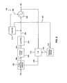
- FIG. 2 is a block diagram of a reference PLL that may be used in the communications device according to an exemplary embodiment of the present invention.
- a reference PLL 200 represents a closed-loop feedback control system that generates the target signal 156 in relation to a frequency and a phase of the reference signal 154. In other words, the reference PLL 200 performs frequency multiplication and/or division, via a negative feedback mechanism, to generate the target signal 156 in terms of the reference signal 154.
- the reference PLL 200 may be implemented using a phase/frequency detector (PFD) 202, a charge pump 204, a loop filter 206, a voltage controlled oscillator (VCO) 208, an optional integer frequency divider 210, an optional dithering module 212, and a controller 214.
- the reference PLL 200 may represent an exemplary embodiment of the reference PLL 108.
- the PFD 202 converts a difference between the frequency and/or the phase of the reference signal 154 and a phase and/or a frequency of a divided feedback signal 258 into an error signal 250. Specifically, the PFD 202 produces the error signal 250 by comparing the frequency and/or the phase of the divided feedback signal 258 and the frequency and/or the phase of the reference signal 154 to detect for deviations between the reference signal 154 and the divided feedback signal 258.
- the reference PLL 200 is in the locked condition. In the locked condition, the error signal 250 is proportional to the phase difference between the reference signal 154 and the divided feedback signal 258.
- the charge pump 204 converts the error signal 250 to a voltage domain representation, denoted as a charge pump output 252, to control the frequency of the VCO 208.
- a charge pump output 252 When the reference PLL 200 is the unlocked condition, the charge pump 204 increases or decreases the charge pump output 252 based on the error signal 250.
- the reference PLL 200 When the reference PLL 200 is in the locked condition the error signal 250 is minimized and the charge pump 204 maintains the charge pump output 252 at a substantially fixed value.
- the loop filter 206 may be used to remove undesirable noise from the charge pump output 252 to generate a tuning signal 254.
- the loop filter 206 may be implemented as a low pass filter to suppress high frequency components in the charge pump output 252 to allow a direct current (DC), or near DC, component of the charge pump output 252 to control the VCO 208.
- the loop filter 206 also maintains stability of the reference PLL 200.
- the VCO 208 is a voltage to frequency converter. Specifically, the VCO 208 produces the target signal 156 based upon the tuning signal 254 and the frequency control signal 268. Typically, the controller 214 adjusts the frequency control signal 268 until the target signal 156 is sufficiently related to the reference signal 154 during the full calibration. For example, the controller 214 may cycle through different combinations of the frequency control signal 268 using a searching algorithm, such as a binary search tree algorithm, a recursion algorithm, a Stern-Brocot algorithm and/or any other suitable search that will be apparent to those skilled in the relevant art(s) without departing from the spirit and scope of the present invention until the target signal 156 is sufficiently related to the reference signal 154.
- a searching algorithm such as a binary search tree algorithm, a recursion algorithm, a Stern-Brocot algorithm and/or any other suitable search that will be apparent to those skilled in the relevant art(s) without departing from the spirit and scope of the present invention until the target signal 156 is sufficiently related to the reference signal 154
- the tuning signal 254 is used to further adjust the target signal 156 until it is approximately equal or an integer or fractional multiple of the reference signal 154.
- the optional integer frequency divider 210 is located in a feedback path of the reference PLL 200.
- the optional integer frequency divider 210 divides the target signal 156 by an integer N to provide the divided feedback signal 258.
- the optional integer frequency divider 210 may adjust the integer N in response to a channel transmission signal 262.
- the optional dithering module 212 allows the reference PLL 200 to dither the divide value over time between two or more integer values to obtain an effective time averaged fractional division factor. More specifically, the optional dithering module 212 randomly selects between the two or more integer values for each iteration of the reference PLL 200 in response to a division code 260, so that on average, a fractional division factor can be represented. The optional dithering module 212 generates the division code 260 in response to the divide ratio control signal 262.
- the controller module 214 calibrates the reference PLL 200 in one of the full calibration, the fine calibration, and/or the offset calibration.
- the controller module 214 illustrates an exemplary implementation of the full calibration, the fine calibration, and/or the offset calibration that were discussed above.
- the controller module 214 initially calibrates the reference PLL 200 to provide the target signal 156 that is proportional to the frequency and/or the phase of the reference signal 154 when a communications device, such as the communications device 100 to provide an example, engages a communications channel.
- the controller module 214 initially calibrates the reference PLL 200 when the communications device is operating in the receive mode of operation.
- the controller module 214 may provide the channel transmission signal 262 that causes the optional dithering module 212 to provide the divide ratio control signal 262 that corresponds to the communications channel.
- the controller module 214 provides a first value for the frequency control signal 268 to cause the VCO 208 to provide the target signal 156 at a first frequency.
- the controller module 214 monitors the tuning signal 254 once the target signal 156 has reached the first frequency.
- the controller module 214 compares the tuning signal 254 to a predetermined tuning signal to determine whether the reference PLL 200 is in the locked condition.
- the predetermined tuning signal represents a pre-known tuning signal that is presented within the reference PLL 200 when the reference PLL 200 is the locked condition.
- the pre-known tuning signal may represent a DC voltage when the reference PLL 200 is the locked condition.
- the controller module 214 compares a magnitude of a difference between the tuning signal 254 and the pre-known tuning signal to a locking threshold. When magnitude of the difference is less than or equal to the locking threshold, the target signal 156 is sufficiently related to the reference signal 154. In this situation, the reference PLL 200 enters in the locked condition to track the reference signal 154.
- the controller module 214 determines whether the second frequency causes the reference PLL 200 to enter into the locked condition. If not, the controller module 214 continues to adjust the frequency control signal 268 until the VCO 208 enters into the locked condition.
- the communications device After receiving communications signals from the communications channel in the receive mode of operation, the communications device may transition from the receive mode of operation to the transmit mode of operation. After transmitting communications signal onto the communications channel, the communications device may transition from the transmit mode of operation back to the receive mode of operation or engage another communications channel.
- the controller module 214 may calibrate the reference PLL 200 using the fine calibration, and/or the offset calibration while the communications device is transitioning between these modes of operation. Typically, selection of the fine calibration and or the offset calibration is based on the communications standard in which the communications device is operating.
- the communications device may be operating in the LTE TDD standard.
- the LTE TDD standard allows 71.3 microseconds for the controller module 214 to calibrate the VCO 208 so that the reference PLL 200 locks onto the reference signal 154.
- the controller module 214 selects the fine calibration when the communications device is transitioning from the receive mode of operation to the transmit mode of operation.
- the communications device may be operating in the TD-SCDMA standard.
- the TD-SCDMA standard allows 12.5 microseconds for the controller module 214 to calibrate the VCO 208 so that the reference PLL 200 locks onto the reference signal 154.
- the controller module 214 selects the offset calibration when the communications device is transitioning from the transmit mode of operation to the receive mode of operation because the LTE TDD standard provides sufficient time to complete the offset calibration but not sufficient time to complete the fine calibration.
- the controller module 214 performs the offset calibration by adjusting the target signal 156 by the predetermined amount that relates to a shifting of the target signal 156 that results from transitioning between modes of operation.
- the predetermined amount represents a predetermined voltage and/or current that is coupled onto the tuning signal 254. This predetermined voltage and/or current shifts the target signal 156 to accommodate for the difference that results from transitioning between modes of operation.
- the reference PLL 200 settles to the locked condition within the duration of time specified by the communications standards.
- the fine calibration includes the offset calibration, as discussed above, as well as another adjustment of the target frequency 156 to compensate for operational conditions, such as temperature to provide an example, of the communications device.
- the controller module 214 adjusts the target signal 156 by the predetermined amount in a substantially similar manner as the offset calibration.
- the controller module 214 additionally adjusts the target signal 156 to compensate for the operational conditions. Typically, this operational adjustment may be characterized as being similar to the full calibration, but scaled down.
- the controller module 214 provides a predetermined number of different values for the frequency control signal 268 to cause the VCO 208 to provide the target signal 156 at different frequencies. In an exemplary embodiment, the predetermined number of different values represents two different combinations of the searching algorithm.
- the predetermined number of different values may represent any suitable number of different combinations of the searching algorithm so long as the fine calibration is completed within the time allotted by the communications standard without departing from the spirit and scope of the present invention.
- FIG. 3 is a table that represents each type of calibration that may be used by the communications device for different communications standards according to an exemplary embodiment of the present invention.
- FIG. 3 includes exemplary communications standards in which a communications device, such as the communications device 100 to provide an example may operate in; however, those skilled in the relevant art(s) will recognize that the communications device may operate in accordance with other communications standards without departing from the spirit and scope of the present invention.
- FIG. 3 depicts the time allowed by each respective communications standard for a controller module, such as the controller module 120 or the controller module 214 to provide some examples, to calibrate a reference PLL, such as the reference PLL 108 or the reference PLL 200 to provide some examples.
- a controller module such as the controller module 120 or the controller module 214 to provide some examples
- a reference PLL such as the reference PLL 108 or the reference PLL 200 to provide some examples.
- FIG. 3 depicts that the TD-SCDMA communications standard allows 200 microseconds for the controller module to properly calibrate the reference PLL when the communications device engages a communications channel.
- the 200 microseconds provided by the TD-SCDMA communications standard may be sufficient to perform the full calibration.
- the calibration period for the transition from the receive mode of operation to the transmit mode of operation provided by the TD-SCDMA is 75 microseconds.
- the 75 microseconds may be sufficient to perform the fine calibration but not sufficient to perform the full calibration.
- the calibration period for the transition from the transmit mode of operation to the receive mode of operation provided by the TD-SCDMA is 12.5 microseconds.
- the 12.5 microseconds may be sufficient to perform the offset calibration but not sufficient to perform the full calibration and/or the fine calibration.
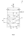
- FIG. 4 illustrates a block diagram of an exemplary voltage controlled oscillator (VCO) that may be used in the communications device according to an exemplary embodiment of the present invention.
- a controller module such as the controller module 120 or the controller module 214 to provide some examples, calibrates a VCO 400 in one of the full calibration, the fine calibration, and/or the offset calibration to provide target outputs 452.1 and 452.2.
- the target outputs 452.1 and 452.2 represent an exemplary embodiment of the target output 156.
- the VCO 400 includes a fine frequency component 402 and a course frequency component 404 which operate in conjunction with each other to provide the target signal 156.
- the fine frequency component 402 includes a first fine capacitor 406.1, a second fine capacitor 406.2, and a varactor diode 408. As shown in FIG. 4 , the tuning signal 254 is applied to the varactor diode 408.
- the varactor diode 408 represents a variable capacitance whose capacitance is a function of the tuning signal 254.
- the first fine capacitor 406.1 and the second fine capacitor 406.2 are coupled the varactor diode 408 to isolate the tuning signal 254 from the course frequency component 404.
- the first fine capacitor 406.1 and the second fine capacitor 406.2 represent large capacitors when compared to the varactor diode 408 such that a capacitance of the fine frequency component 402 is dominated by the varactor diode 408.
- the course frequency component 404 includes transistor switches 410.1 through 410. n , first capacitors 412.1 through 412. n , second capacitors 414.1 through 414. n , a first inductor 416.1 and a second inductor 416.2.
- the switches 410.1 through 410. n cause their corresponding first capacitors 412.1 through 412. n and second capacitors 414.1 through 414. n to contribute to a capacitance of the course frequency component 404 when activated by a corresponding frequency control signal 450.1 through 450. n .
- the frequency control signals 450.1 through 450. n represent an exemplary embodiment of the frequency control signal 268. In other words, the first capacitors 412.1 through 412. n and second capacitors 414.1 through 414.
- the course frequency component 404 may include first capacitors 412.1 through 412.8 and second capacitors 414.1 through 414.8. Those capacitors that are switched in the course frequency component 404 contribute to the capacitance of the course frequency component 404 while those capacitors that are switched out of the course frequency component 404 do not.
- the first inductor 416.1, the second inductor 416.2, and the first capacitors 412.1 through 412. n and the second capacitors 414.1 through 414. n that are switched in the course frequency component 404 are configured and arranged to form a resonant circuit.
- the VCO 400 may include optionally a biasing circuit that includes a first biasing transistor 418.1, a second biasing transistor 418.2, and a biasing current source 420.
- the controller module provides various frequency control signal 450.1 through 450. n to switch various first capacitors 412.1 through 412. n and various second capacitors 414.1 through 414. n in and out of the course frequency component 404 during the full calibration.
- the various frequency control signals 450.1 through 450. n are determined in accordance with the searching algorithm.
- the switching in and out of the first capacitors 412.1 through 412. n and the second capacitors 414.1 through 414. n in this manner adjusts a frequency of the target outputs 452.1 and 452.2.
- the frequency of the target outputs 452.1 and 452.2 is inversely related to the capacitance of the course frequency component 404.
- the controller module continuously switches the first capacitors 412.1 through 412. n and the second capacitors 414.1 through 414.
- the controller module adjusts the capacitance of the fine frequency component 402 by the predetermined amount during the offset calibration without adjusting the capacitance of the course frequency component 404.
- the controller module adjusts the capacitance of the fine frequency component 402 by the predetermined amount and adjusts the frequency control signals 450.1 through 450. n by the predetermined number of different values to adjust the capacitance of the course frequency component 404 to compensate during the fine calibration.
- FIG. 5 is a flowchart of exemplary operational steps of the communications device according to an exemplary embodiment of the present invention.
- the present invention is not limited to this operational description. Rather, it will be apparent to persons skilled in the relevant art(s) from the teachings herein that other operational control flows are within the scope and spirit of the present invention. The following discussion describes the steps in FIG. 5 .
- the operational control flow determines a communications channel from among a plurality of communications channels that is to be used by a communications device to transmit and/or receive a communications signal.
- the operational control flow performs the full calibration to calibrate the communications device for the communications channel. Specifically, the operational control flow adjusts a reference PLL, such as the reference PLL 108 or the reference PLL 200 to provide some examples, within the communications device to lock onto a reference signal, such as reference signal 154 to provide an example.
- a reference PLL such as the reference PLL 108 or the reference PLL 200
- the operational control flow receives the communications signal from step 510 from the communications channel from step 510 and/or transmits the communications signal from step 510 onto the communications channel from step 510.
- the operational control flows determines whether the communications device is to select another communications channel from among the plurality of communications channels or to transition from the receive mode of operation to the transmit mode of operation or from the transmit mode of operation to the receive mode of operation. For example, the operational control flow determines whether the communications device is to subsequently transmit another communications onto the communications channel from step 510 after receiving the communications signal from step 510 from the communications channel from step 510. As another example, the operational control flow determines whether the communications device is to subsequently receive another communications from the communications channel from step 510 after transmit the communications signal from step 510 onto the communications channel from step 510.
- step 550 The operational control flow proceeds to step 550 to transition between these modes of operation or reverts back to step 510 to select another communications channel.
- step 540 the operational control flow determines whether the communications device is to transition between the modes of operation of step 530. If so, the operational control flow proceeds to step 550, otherwise, the operational control reverts to step 510 to determine another communications signal.
- the operational control flow determines the operation transition time allowed by a communications standard. For example, the operational control flow transitions from the transmit mode of operation to the receive mode of operation while operating in the TD-SCDMA communications standard. In this example, the operational control flow determines the transition time allowed by the TD-SCDMA communications standard to transition from the transmit mode of operation to the receive mode of operation which is approximately 12.5 microseconds.
- the operational control flow determines whether the communications standard provides sufficient time to calibrate the communications device using the fine calibration. If so, the operational control flow proceeds to step 570. Otherwise, the operational control flow proceeds to step 580.
- step 570 the operational control flow performs the fine calibration then reverts to step 540.
- step 580 the operational control flow performs the offset calibration then reverts to step 540.
Landscapes
- Engineering & Computer Science (AREA)
- Computer Networks & Wireless Communication (AREA)
- Signal Processing (AREA)
- Power Engineering (AREA)
- Stabilization Of Oscillater, Synchronisation, Frequency Synthesizers (AREA)
Applications Claiming Priority (2)
| Application Number | Priority Date | Filing Date | Title |
|---|---|---|---|
| US201161556094P | 2011-11-04 | 2011-11-04 | |
| US13/356,137 US8611842B2 (en) | 2011-11-04 | 2012-01-23 | Apparatus and method for fast phase locked loop (PLL) settling for cellular time-division duplex (TDD) communications systems |
Publications (3)
| Publication Number | Publication Date |
|---|---|
| EP2590263A2 true EP2590263A2 (de) | 2013-05-08 |
| EP2590263A3 EP2590263A3 (de) | 2017-08-02 |
| EP2590263B1 EP2590263B1 (de) | 2018-09-19 |
Family
ID=47225875
Family Applications (1)
| Application Number | Title | Priority Date | Filing Date |
|---|---|---|---|
| EP12007351.5A Active EP2590263B1 (de) | 2011-11-04 | 2012-10-25 | Vorrichtung und Verfahren zum Einstellen eines Phasenregelkreises (PLL) für ein zelluläres Zeitteilungsduplex (TDD)-Kommunikationssystem |
Country Status (5)
| Country | Link |
|---|---|
| US (1) | US8611842B2 (de) |
| EP (1) | EP2590263B1 (de) |
| KR (1) | KR101436979B1 (de) |
| CN (1) | CN103095291B (de) |
| TW (1) | TWI462498B (de) |
Families Citing this family (9)
| Publication number | Priority date | Publication date | Assignee | Title |
|---|---|---|---|---|
| KR102481291B1 (ko) | 2016-09-12 | 2022-12-26 | 삼성전자 주식회사 | 비 면허 대역을 사용하는 무선 통신 시스템에서 안테나 위상을 교정하는 방법 및 장치 |
| KR102520406B1 (ko) | 2016-12-23 | 2023-04-12 | 삼성전자 주식회사 | 대용량 안테나 시스템에서 안테나 위상 보정 방법 및 장치 |
| GB201810760D0 (en) * | 2018-06-29 | 2018-08-15 | Nordic Semiconductor Asa | Calibration of a synthersiser in a radio receiver |
| JP7104407B2 (ja) * | 2018-07-25 | 2022-07-21 | ザインエレクトロニクス株式会社 | 電圧制御発振器、pll回路およびcdr装置 |
| KR102785637B1 (ko) | 2019-12-19 | 2025-03-26 | 삼성전자주식회사 | 전자 장치에서의 소손 방지 회로 및 이를 위한 방법 |
| CN111900978B (zh) * | 2020-08-07 | 2021-11-23 | 上海橙群微电子有限公司 | 锁相环电路、发射机和无线收发系统 |
| KR102878678B1 (ko) * | 2021-05-10 | 2025-10-31 | 삼성전자주식회사 | 위상 고정 루프 및 위상 고정 루프의 동작 방법 |
| CN114401001B (zh) * | 2021-12-30 | 2022-11-15 | 北京力通通信有限公司 | 一种锁相环快速锁相方法 |
| CN121396157B (zh) * | 2025-12-24 | 2026-04-10 | 无锡国芯微高新技术有限公司 | 一种提高psi5通信时序精度的方法和电路 |
Family Cites Families (11)
| Publication number | Priority date | Publication date | Assignee | Title |
|---|---|---|---|---|
| KR100219709B1 (ko) * | 1994-03-15 | 1999-09-01 | 윤종용 | 디지탈무선통신장치에있어서송수신신호처리회로 |
| JP2929984B2 (ja) * | 1995-11-28 | 1999-08-03 | 関西日本電気株式会社 | Pllシンセサイザ回路 |
| US7546097B2 (en) * | 2002-03-06 | 2009-06-09 | Qualcomm Incorporated | Calibration techniques for frequency synthesizers |
| GB2413019B (en) * | 2002-05-31 | 2006-03-29 | Renesas Tech Corp | Semiconductor integrated circuit device for communication |
| TW200516844A (en) * | 2003-09-10 | 2005-05-16 | Koninkl Philips Electronics Nv | Variable impedance circuit using unary cells |
| EP1698056A1 (de) * | 2003-12-19 | 2006-09-06 | Philips Intellectual Property & Standards GmbH | Verfahren und anordnung zur störungskompensation in einem spannungsgesteuerten frequenzgenerator |
| KR101069231B1 (ko) * | 2004-02-20 | 2011-10-04 | 지씨티 세미컨덕터 인코포레이티드 | Lc오실레이터를 사용한 주파수 발생기 튜닝 시스템 및 방법 |
| KR100793988B1 (ko) * | 2006-04-21 | 2008-01-16 | 삼성전자주식회사 | 자기 교정 전압 제어 발진기를 위한 시스템 및 방법 |
| US8010072B1 (en) * | 2008-06-18 | 2011-08-30 | Atheros Communications, Inc. | Charge pump current compensation for phase-locked loop frequency synthesizer systems |
| US8130046B2 (en) * | 2009-03-19 | 2012-03-06 | Qualcomm Incorporated | Frequency calibration of radio frequency oscillators |
| US8098110B2 (en) * | 2009-11-20 | 2012-01-17 | Qualcomm Incorporated | Phase locked loop apparatus with selectable capacitance device |
-
2012
- 2012-01-23 US US13/356,137 patent/US8611842B2/en active Active
- 2012-10-25 EP EP12007351.5A patent/EP2590263B1/de active Active
- 2012-11-02 TW TW101140737A patent/TWI462498B/zh not_active IP Right Cessation
- 2012-11-05 KR KR1020120124360A patent/KR101436979B1/ko not_active Expired - Fee Related
- 2012-11-05 CN CN201210436456.3A patent/CN103095291B/zh active Active
Non-Patent Citations (1)
| Title |
|---|
| None |
Also Published As
| Publication number | Publication date |
|---|---|
| CN103095291B (zh) | 2016-06-29 |
| EP2590263B1 (de) | 2018-09-19 |
| KR20130049761A (ko) | 2013-05-14 |
| US20130113535A1 (en) | 2013-05-09 |
| US8611842B2 (en) | 2013-12-17 |
| HK1180464A1 (zh) | 2013-10-18 |
| KR101436979B1 (ko) | 2014-11-03 |
| CN103095291A (zh) | 2013-05-08 |
| TWI462498B (zh) | 2014-11-21 |
| TW201325106A (zh) | 2013-06-16 |
| EP2590263A3 (de) | 2017-08-02 |
Similar Documents
| Publication | Publication Date | Title |
|---|---|---|
| EP2590263B1 (de) | Vorrichtung und Verfahren zum Einstellen eines Phasenregelkreises (PLL) für ein zelluläres Zeitteilungsduplex (TDD)-Kommunikationssystem | |
| US8954017B2 (en) | Clock signal multiplication to reduce noise coupled onto a transmission communication signal of a communications device | |
| US7486147B2 (en) | Low phase noise phase locked loops with minimum lock time | |
| US8350608B2 (en) | Phase locked loop circuit including automatic frequency control circuit and operating method thereof | |
| US7868672B2 (en) | Digital phase-locked loop with two-point modulation and adaptive delay matching | |
| US7994867B2 (en) | Oscillator control apparatus | |
| US9203416B2 (en) | Compensation of slow time-varying variations in voltage controlled oscillator (VCO) frequency in cellular transceivers | |
| US20110260763A1 (en) | Frequency synthesizer | |
| TWI285027B (en) | Phase-locked loops | |
| KR100306671B1 (ko) | Pll신디사이저및그제어방법 | |
| US8988122B2 (en) | Apparatus and method for performing spread-spectrum clock control | |
| US7103127B2 (en) | System for controlling the frequency of an oscillator | |
| US20090201094A1 (en) | Phase comparison circuit and pll synthesizer using the same | |
| TW521504B (en) | Auto calibration circuit for radio frequency synthesizer circuits | |
| US20130271229A1 (en) | Method and apparatus for local oscillator | |
| US20110080196A1 (en) | VCO Control Circuit and Method Thereof, Fast Locking PLL and Method for Fast Locking PLL | |
| CN114301456A (zh) | 锁相环电路、时钟发生器及电子设备 | |
| US20090206894A1 (en) | Phase-Locked Loop with Adaptive Performance | |
| US20080036544A1 (en) | Method for adjusting oscillator in phase-locked loop and related frequency synthesizer | |
| WO2001093418A2 (en) | Linear dead-band-free digital phase detection | |
| US10122370B2 (en) | High impedance passive switched capacitor common mode feedback network | |
| KR100806506B1 (ko) | 위상 동기 루프 및 무선 전기 신호 수신 장치 | |
| HK1180464B (en) | Fast phase locked loop (pll) settling | |
| US9071255B2 (en) | Phase locked loop and associated phase alignment method | |
| US9467156B2 (en) | Frequency synthesizing module and related frequency gain determining method |
Legal Events
| Date | Code | Title | Description |
|---|---|---|---|
| PUAI | Public reference made under article 153(3) epc to a published international application that has entered the european phase |
Free format text: ORIGINAL CODE: 0009012 |
|
| 17P | Request for examination filed |
Effective date: 20121025 |
|
| AK | Designated contracting states |
Kind code of ref document: A2 Designated state(s): AL AT BE BG CH CY CZ DE DK EE ES FI FR GB GR HR HU IE IS IT LI LT LU LV MC MK MT NL NO PL PT RO RS SE SI SK SM TR |
|
| AX | Request for extension of the european patent |
Extension state: BA ME |
|
| PUAL | Search report despatched |
Free format text: ORIGINAL CODE: 0009013 |
|
| RAP1 | Party data changed (applicant data changed or rights of an application transferred) |
Owner name: AVAGO TECHNOLOGIES GENERAL IP (SINGAPORE) PTE. LTD |
|
| AK | Designated contracting states |
Kind code of ref document: A3 Designated state(s): AL AT BE BG CH CY CZ DE DK EE ES FI FR GB GR HR HU IE IS IT LI LT LU LV MC MK MT NL NO PL PT RO RS SE SI SK SM TR |
|
| AX | Request for extension of the european patent |
Extension state: BA ME |
|
| RIC1 | Information provided on ipc code assigned before grant |
Ipc: H03L 7/197 20060101ALI20170628BHEP Ipc: H04B 1/40 20150101AFI20170628BHEP Ipc: H03L 7/099 20060101ALI20170628BHEP Ipc: H03L 7/10 20060101ALI20170628BHEP |
|
| 17Q | First examination report despatched |
Effective date: 20170724 |
|
| RBV | Designated contracting states (corrected) |
Designated state(s): AL AT BE BG CH CY CZ DE DK EE ES FI FR GB GR HR HU IE IS IT LI LT LU LV MC MK MT NL NO PL PT RO RS SE SI SK SM TR |
|
| REG | Reference to a national code |
Ref country code: DE Ref legal event code: R079 Ref document number: 602012051172 Country of ref document: DE Free format text: PREVIOUS MAIN CLASS: H01Q0009040000 Ipc: H03L0007100000 |
|
| GRAP | Despatch of communication of intention to grant a patent |
Free format text: ORIGINAL CODE: EPIDOSNIGR1 |
|
| RIC1 | Information provided on ipc code assigned before grant |
Ipc: H03L 7/10 20060101AFI20180329BHEP Ipc: H04B 1/403 20150101ALI20180329BHEP Ipc: H03L 7/099 20060101ALN20180329BHEP Ipc: H03L 7/197 20060101ALI20180329BHEP |
|
| RIC1 | Information provided on ipc code assigned before grant |
Ipc: H03L 7/197 20060101ALI20180410BHEP Ipc: H03L 7/10 20060101AFI20180410BHEP Ipc: H03L 7/099 20060101ALN20180410BHEP Ipc: H04B 1/403 20150101ALI20180410BHEP |
|
| INTG | Intention to grant announced |
Effective date: 20180430 |
|
| GRAS | Grant fee paid |
Free format text: ORIGINAL CODE: EPIDOSNIGR3 |
|
| GRAA | (expected) grant |
Free format text: ORIGINAL CODE: 0009210 |
|
| AK | Designated contracting states |
Kind code of ref document: B1 Designated state(s): AL AT BE BG CH CY CZ DE DK EE ES FI FR GB GR HR HU IE IS IT LI LT LU LV MC MK MT NL NO PL PT RO RS SE SI SK SM TR |
|
| REG | Reference to a national code |
Ref country code: GB Ref legal event code: FG4D |
|
| REG | Reference to a national code |
Ref country code: CH Ref legal event code: EP |
|
| REG | Reference to a national code |
Ref country code: AT Ref legal event code: REF Ref document number: 1044449 Country of ref document: AT Kind code of ref document: T Effective date: 20181015 |
|
| REG | Reference to a national code |
Ref country code: IE Ref legal event code: FG4D |
|
| REG | Reference to a national code |
Ref country code: DE Ref legal event code: R096 Ref document number: 602012051172 Country of ref document: DE |
|
| REG | Reference to a national code |
Ref country code: DE Ref legal event code: R081 Ref document number: 602012051172 Country of ref document: DE Owner name: AVAGO TECHNOLOGIES INTERNATIONAL SALES PTE. LT, SG Free format text: FORMER OWNER: AVAGO TECHNOLOGIES GENERAL IP (SINGAPORE) PTE. LTD., SINGAPORE, SG Ref country code: DE Ref legal event code: R082 Ref document number: 602012051172 Country of ref document: DE Representative=s name: BOSCH JEHLE PATENTANWALTSGESELLSCHAFT MBH, DE |
|
| RAP2 | Party data changed (patent owner data changed or rights of a patent transferred) |
Owner name: AVAGO TECHNOLOGIES INTERNATIONAL SALES PTE. LIMITE |
|
| REG | Reference to a national code |
Ref country code: NL Ref legal event code: MP Effective date: 20180919 |
|
| PG25 | Lapsed in a contracting state [announced via postgrant information from national office to epo] |
Ref country code: FI Free format text: LAPSE BECAUSE OF FAILURE TO SUBMIT A TRANSLATION OF THE DESCRIPTION OR TO PAY THE FEE WITHIN THE PRESCRIBED TIME-LIMIT Effective date: 20180919 Ref country code: GR Free format text: LAPSE BECAUSE OF FAILURE TO SUBMIT A TRANSLATION OF THE DESCRIPTION OR TO PAY THE FEE WITHIN THE PRESCRIBED TIME-LIMIT Effective date: 20181220 Ref country code: RS Free format text: LAPSE BECAUSE OF FAILURE TO SUBMIT A TRANSLATION OF THE DESCRIPTION OR TO PAY THE FEE WITHIN THE PRESCRIBED TIME-LIMIT Effective date: 20180919 Ref country code: SE Free format text: LAPSE BECAUSE OF FAILURE TO SUBMIT A TRANSLATION OF THE DESCRIPTION OR TO PAY THE FEE WITHIN THE PRESCRIBED TIME-LIMIT Effective date: 20180919 Ref country code: NO Free format text: LAPSE BECAUSE OF FAILURE TO SUBMIT A TRANSLATION OF THE DESCRIPTION OR TO PAY THE FEE WITHIN THE PRESCRIBED TIME-LIMIT Effective date: 20181219 Ref country code: LT Free format text: LAPSE BECAUSE OF FAILURE TO SUBMIT A TRANSLATION OF THE DESCRIPTION OR TO PAY THE FEE WITHIN THE PRESCRIBED TIME-LIMIT Effective date: 20180919 Ref country code: BG Free format text: LAPSE BECAUSE OF FAILURE TO SUBMIT A TRANSLATION OF THE DESCRIPTION OR TO PAY THE FEE WITHIN THE PRESCRIBED TIME-LIMIT Effective date: 20181219 |
|
| REG | Reference to a national code |
Ref country code: LT Ref legal event code: MG4D |
|
| PG25 | Lapsed in a contracting state [announced via postgrant information from national office to epo] |
Ref country code: LV Free format text: LAPSE BECAUSE OF FAILURE TO SUBMIT A TRANSLATION OF THE DESCRIPTION OR TO PAY THE FEE WITHIN THE PRESCRIBED TIME-LIMIT Effective date: 20180919 Ref country code: HR Free format text: LAPSE BECAUSE OF FAILURE TO SUBMIT A TRANSLATION OF THE DESCRIPTION OR TO PAY THE FEE WITHIN THE PRESCRIBED TIME-LIMIT Effective date: 20180919 Ref country code: AL Free format text: LAPSE BECAUSE OF FAILURE TO SUBMIT A TRANSLATION OF THE DESCRIPTION OR TO PAY THE FEE WITHIN THE PRESCRIBED TIME-LIMIT Effective date: 20180919 |
|
| REG | Reference to a national code |
Ref country code: AT Ref legal event code: MK05 Ref document number: 1044449 Country of ref document: AT Kind code of ref document: T Effective date: 20180919 |
|
| PG25 | Lapsed in a contracting state [announced via postgrant information from national office to epo] |
Ref country code: IS Free format text: LAPSE BECAUSE OF FAILURE TO SUBMIT A TRANSLATION OF THE DESCRIPTION OR TO PAY THE FEE WITHIN THE PRESCRIBED TIME-LIMIT Effective date: 20190119 Ref country code: RO Free format text: LAPSE BECAUSE OF FAILURE TO SUBMIT A TRANSLATION OF THE DESCRIPTION OR TO PAY THE FEE WITHIN THE PRESCRIBED TIME-LIMIT Effective date: 20180919 Ref country code: ES Free format text: LAPSE BECAUSE OF FAILURE TO SUBMIT A TRANSLATION OF THE DESCRIPTION OR TO PAY THE FEE WITHIN THE PRESCRIBED TIME-LIMIT Effective date: 20180919 Ref country code: NL Free format text: LAPSE BECAUSE OF FAILURE TO SUBMIT A TRANSLATION OF THE DESCRIPTION OR TO PAY THE FEE WITHIN THE PRESCRIBED TIME-LIMIT Effective date: 20180919 Ref country code: CZ Free format text: LAPSE BECAUSE OF FAILURE TO SUBMIT A TRANSLATION OF THE DESCRIPTION OR TO PAY THE FEE WITHIN THE PRESCRIBED TIME-LIMIT Effective date: 20180919 Ref country code: PL Free format text: LAPSE BECAUSE OF FAILURE TO SUBMIT A TRANSLATION OF THE DESCRIPTION OR TO PAY THE FEE WITHIN THE PRESCRIBED TIME-LIMIT Effective date: 20180919 Ref country code: EE Free format text: LAPSE BECAUSE OF FAILURE TO SUBMIT A TRANSLATION OF THE DESCRIPTION OR TO PAY THE FEE WITHIN THE PRESCRIBED TIME-LIMIT Effective date: 20180919 Ref country code: AT Free format text: LAPSE BECAUSE OF FAILURE TO SUBMIT A TRANSLATION OF THE DESCRIPTION OR TO PAY THE FEE WITHIN THE PRESCRIBED TIME-LIMIT Effective date: 20180919 Ref country code: IT Free format text: LAPSE BECAUSE OF FAILURE TO SUBMIT A TRANSLATION OF THE DESCRIPTION OR TO PAY THE FEE WITHIN THE PRESCRIBED TIME-LIMIT Effective date: 20180919 |
|
| PG25 | Lapsed in a contracting state [announced via postgrant information from national office to epo] |
Ref country code: SK Free format text: LAPSE BECAUSE OF FAILURE TO SUBMIT A TRANSLATION OF THE DESCRIPTION OR TO PAY THE FEE WITHIN THE PRESCRIBED TIME-LIMIT Effective date: 20180919 Ref country code: PT Free format text: LAPSE BECAUSE OF FAILURE TO SUBMIT A TRANSLATION OF THE DESCRIPTION OR TO PAY THE FEE WITHIN THE PRESCRIBED TIME-LIMIT Effective date: 20190119 Ref country code: SM Free format text: LAPSE BECAUSE OF FAILURE TO SUBMIT A TRANSLATION OF THE DESCRIPTION OR TO PAY THE FEE WITHIN THE PRESCRIBED TIME-LIMIT Effective date: 20180919 |
|
| REG | Reference to a national code |
Ref country code: CH Ref legal event code: PL |
|
| REG | Reference to a national code |
Ref country code: DE Ref legal event code: R097 Ref document number: 602012051172 Country of ref document: DE |
|
| REG | Reference to a national code |
Ref country code: BE Ref legal event code: MM Effective date: 20181031 |
|
| PG25 | Lapsed in a contracting state [announced via postgrant information from national office to epo] |
Ref country code: LU Free format text: LAPSE BECAUSE OF NON-PAYMENT OF DUE FEES Effective date: 20181025 |
|
| REG | Reference to a national code |
Ref country code: IE Ref legal event code: MM4A |
|
| PLBE | No opposition filed within time limit |
Free format text: ORIGINAL CODE: 0009261 |
|
| STAA | Information on the status of an ep patent application or granted ep patent |
Free format text: STATUS: NO OPPOSITION FILED WITHIN TIME LIMIT |
|
| PG25 | Lapsed in a contracting state [announced via postgrant information from national office to epo] |
Ref country code: MC Free format text: LAPSE BECAUSE OF FAILURE TO SUBMIT A TRANSLATION OF THE DESCRIPTION OR TO PAY THE FEE WITHIN THE PRESCRIBED TIME-LIMIT Effective date: 20180919 Ref country code: DK Free format text: LAPSE BECAUSE OF FAILURE TO SUBMIT A TRANSLATION OF THE DESCRIPTION OR TO PAY THE FEE WITHIN THE PRESCRIBED TIME-LIMIT Effective date: 20180919 |
|
| 26N | No opposition filed |
Effective date: 20190620 |
|
| GBPC | Gb: european patent ceased through non-payment of renewal fee |
Effective date: 20181219 |
|
| PG25 | Lapsed in a contracting state [announced via postgrant information from national office to epo] |
Ref country code: CH Free format text: LAPSE BECAUSE OF NON-PAYMENT OF DUE FEES Effective date: 20181031 Ref country code: BE Free format text: LAPSE BECAUSE OF NON-PAYMENT OF DUE FEES Effective date: 20181031 Ref country code: LI Free format text: LAPSE BECAUSE OF NON-PAYMENT OF DUE FEES Effective date: 20181031 |
|
| PG25 | Lapsed in a contracting state [announced via postgrant information from national office to epo] |
Ref country code: FR Free format text: LAPSE BECAUSE OF NON-PAYMENT OF DUE FEES Effective date: 20181119 Ref country code: SI Free format text: LAPSE BECAUSE OF FAILURE TO SUBMIT A TRANSLATION OF THE DESCRIPTION OR TO PAY THE FEE WITHIN THE PRESCRIBED TIME-LIMIT Effective date: 20180919 Ref country code: IE Free format text: LAPSE BECAUSE OF NON-PAYMENT OF DUE FEES Effective date: 20181025 |
|
| PG25 | Lapsed in a contracting state [announced via postgrant information from national office to epo] |
Ref country code: GB Free format text: LAPSE BECAUSE OF NON-PAYMENT OF DUE FEES Effective date: 20181219 |
|
| PG25 | Lapsed in a contracting state [announced via postgrant information from national office to epo] |
Ref country code: MT Free format text: LAPSE BECAUSE OF NON-PAYMENT OF DUE FEES Effective date: 20181025 |
|
| PG25 | Lapsed in a contracting state [announced via postgrant information from national office to epo] |
Ref country code: TR Free format text: LAPSE BECAUSE OF FAILURE TO SUBMIT A TRANSLATION OF THE DESCRIPTION OR TO PAY THE FEE WITHIN THE PRESCRIBED TIME-LIMIT Effective date: 20180919 |
|
| PG25 | Lapsed in a contracting state [announced via postgrant information from national office to epo] |
Ref country code: MK Free format text: LAPSE BECAUSE OF NON-PAYMENT OF DUE FEES Effective date: 20180919 Ref country code: CY Free format text: LAPSE BECAUSE OF FAILURE TO SUBMIT A TRANSLATION OF THE DESCRIPTION OR TO PAY THE FEE WITHIN THE PRESCRIBED TIME-LIMIT Effective date: 20180919 Ref country code: HU Free format text: LAPSE BECAUSE OF FAILURE TO SUBMIT A TRANSLATION OF THE DESCRIPTION OR TO PAY THE FEE WITHIN THE PRESCRIBED TIME-LIMIT; INVALID AB INITIO Effective date: 20121025 |
|
| PGFP | Annual fee paid to national office [announced via postgrant information from national office to epo] |
Ref country code: DE Payment date: 20251010 Year of fee payment: 14 |