EP2590308A2 - Stromversorgungssystem, Bilderzeugungsvorrichtung damit, und Netzteilschaltung mit niedriger Kapazität - Google Patents
Stromversorgungssystem, Bilderzeugungsvorrichtung damit, und Netzteilschaltung mit niedriger Kapazität Download PDFInfo
- Publication number
- EP2590308A2 EP2590308A2 EP12186338.5A EP12186338A EP2590308A2 EP 2590308 A2 EP2590308 A2 EP 2590308A2 EP 12186338 A EP12186338 A EP 12186338A EP 2590308 A2 EP2590308 A2 EP 2590308A2
- Authority
- EP
- European Patent Office
- Prior art keywords
- power supply
- zero
- circuit
- crossing
- voltage
- Prior art date
- Legal status (The legal status is an assumption and is not a legal conclusion. Google has not performed a legal analysis and makes no representation as to the accuracy of the status listed.)
- Granted
Links
Images


Classifications
-
- G—PHYSICS
- G03—PHOTOGRAPHY; CINEMATOGRAPHY; ANALOGOUS TECHNIQUES USING WAVES OTHER THAN OPTICAL WAVES; ELECTROGRAPHY; HOLOGRAPHY
- G03G—ELECTROGRAPHY; ELECTROPHOTOGRAPHY; MAGNETOGRAPHY
- G03G15/00—Apparatus for electrographic processes using a charge pattern
- G03G15/50—Machine control of apparatus for electrographic processes using a charge pattern, e.g. regulating differents parts of the machine, multimode copiers, microprocessor control
- G03G15/5004—Power supply control, e.g. power-saving mode, automatic power turn-off
-
- G—PHYSICS
- G03—PHOTOGRAPHY; CINEMATOGRAPHY; ANALOGOUS TECHNIQUES USING WAVES OTHER THAN OPTICAL WAVES; ELECTROGRAPHY; HOLOGRAPHY
- G03G—ELECTROGRAPHY; ELECTROPHOTOGRAPHY; MAGNETOGRAPHY
- G03G15/00—Apparatus for electrographic processes using a charge pattern
- G03G15/80—Details relating to power supplies, circuits boards, electrical connections
-
- H—ELECTRICITY
- H02—GENERATION; CONVERSION OR DISTRIBUTION OF ELECTRIC POWER
- H02M—APPARATUS FOR CONVERSION BETWEEN AC AND AC, BETWEEN AC AND DC, OR BETWEEN DC AND DC, AND FOR USE WITH MAINS OR SIMILAR POWER SUPPLY SYSTEMS; CONVERSION OF DC OR AC INPUT POWER INTO SURGE OUTPUT POWER; CONTROL OR REGULATION THEREOF
- H02M7/00—Conversion of AC power input into DC power output; Conversion of DC power input into AC power output
- H02M7/02—Conversion of AC power input into DC power output without possibility of reversal
- H02M7/04—Conversion of AC power input into DC power output without possibility of reversal by static converters
- H02M7/06—Conversion of AC power input into DC power output without possibility of reversal by static converters using discharge tubes without control electrode or semiconductor devices without control electrode
-
- G—PHYSICS
- G01—MEASURING; TESTING
- G01R—MEASURING ELECTRIC VARIABLES; MEASURING MAGNETIC VARIABLES
- G01R19/00—Arrangements for measuring currents or voltages or for indicating presence or sign thereof
- G01R19/175—Indicating the instants of passage of current or voltage through a given value, e.g. passage through zero
-
- G—PHYSICS
- G06—COMPUTING OR CALCULATING; COUNTING
- G06F—ELECTRIC DIGITAL DATA PROCESSING
- G06F1/00—Details not covered by groups G06F3/00 - G06F13/00 and G06F21/00
- G06F1/26—Power supply means, e.g. regulation thereof
- G06F1/32—Means for saving power
- G06F1/3203—Power management, i.e. event-based initiation of a power-saving mode
- G06F1/3234—Power saving characterised by the action undertaken
- G06F1/325—Power saving in peripheral device
- G06F1/3284—Power saving in printer
-
- H—ELECTRICITY
- H02—GENERATION; CONVERSION OR DISTRIBUTION OF ELECTRIC POWER
- H02M—APPARATUS FOR CONVERSION BETWEEN AC AND AC, BETWEEN AC AND DC, OR BETWEEN DC AND DC, AND FOR USE WITH MAINS OR SIMILAR POWER SUPPLY SYSTEMS; CONVERSION OF DC OR AC INPUT POWER INTO SURGE OUTPUT POWER; CONTROL OR REGULATION THEREOF
- H02M1/00—Details of apparatus for conversion
- H02M1/0003—Details of control, feedback or regulation circuits
- H02M1/0006—Arrangements for supplying an adequate voltage to the control circuit of converters
-
- H—ELECTRICITY
- H02—GENERATION; CONVERSION OR DISTRIBUTION OF ELECTRIC POWER
- H02M—APPARATUS FOR CONVERSION BETWEEN AC AND AC, BETWEEN AC AND DC, OR BETWEEN DC AND DC, AND FOR USE WITH MAINS OR SIMILAR POWER SUPPLY SYSTEMS; CONVERSION OF DC OR AC INPUT POWER INTO SURGE OUTPUT POWER; CONTROL OR REGULATION THEREOF
- H02M1/00—Details of apparatus for conversion
- H02M1/0003—Details of control, feedback or regulation circuits
- H02M1/0032—Control circuits allowing low power mode operation, e.g. in standby mode
-
- H—ELECTRICITY
- H02—GENERATION; CONVERSION OR DISTRIBUTION OF ELECTRIC POWER
- H02M—APPARATUS FOR CONVERSION BETWEEN AC AND AC, BETWEEN AC AND DC, OR BETWEEN DC AND DC, AND FOR USE WITH MAINS OR SIMILAR POWER SUPPLY SYSTEMS; CONVERSION OF DC OR AC INPUT POWER INTO SURGE OUTPUT POWER; CONTROL OR REGULATION THEREOF
- H02M1/00—Details of apparatus for conversion
- H02M1/0048—Circuits or arrangements for reducing losses
-
- H—ELECTRICITY
- H02—GENERATION; CONVERSION OR DISTRIBUTION OF ELECTRIC POWER
- H02M—APPARATUS FOR CONVERSION BETWEEN AC AND AC, BETWEEN AC AND DC, OR BETWEEN DC AND DC, AND FOR USE WITH MAINS OR SIMILAR POWER SUPPLY SYSTEMS; CONVERSION OF DC OR AC INPUT POWER INTO SURGE OUTPUT POWER; CONTROL OR REGULATION THEREOF
- H02M1/00—Details of apparatus for conversion
- H02M1/0067—Converter structures employing plural converter units, other than for parallel operation of the units on a single load
- H02M1/007—Plural converter units in cascade
-
- H—ELECTRICITY
- H02—GENERATION; CONVERSION OR DISTRIBUTION OF ELECTRIC POWER
- H02M—APPARATUS FOR CONVERSION BETWEEN AC AND AC, BETWEEN AC AND DC, OR BETWEEN DC AND DC, AND FOR USE WITH MAINS OR SIMILAR POWER SUPPLY SYSTEMS; CONVERSION OF DC OR AC INPUT POWER INTO SURGE OUTPUT POWER; CONTROL OR REGULATION THEREOF
- H02M7/00—Conversion of AC power input into DC power output; Conversion of DC power input into AC power output
- H02M7/02—Conversion of AC power input into DC power output without possibility of reversal
- H02M7/04—Conversion of AC power input into DC power output without possibility of reversal by static converters
- H02M7/05—Capacitor coupled rectifiers
-
- Y—GENERAL TAGGING OF NEW TECHNOLOGICAL DEVELOPMENTS; GENERAL TAGGING OF CROSS-SECTIONAL TECHNOLOGIES SPANNING OVER SEVERAL SECTIONS OF THE IPC; TECHNICAL SUBJECTS COVERED BY FORMER USPC CROSS-REFERENCE ART COLLECTIONS [XRACs] AND DIGESTS
- Y02—TECHNOLOGIES OR APPLICATIONS FOR MITIGATION OR ADAPTATION AGAINST CLIMATE CHANGE
- Y02B—CLIMATE CHANGE MITIGATION TECHNOLOGIES RELATED TO BUILDINGS, e.g. HOUSING, HOUSE APPLIANCES OR RELATED END-USER APPLICATIONS
- Y02B70/00—Technologies for an efficient end-user side electric power management and consumption
- Y02B70/10—Technologies improving the efficiency by using switched-mode power supplies [SMPS], i.e. efficient power electronics conversion e.g. power factor correction or reduction of losses in power supplies or efficient standby modes
Definitions
- the present disclosure relates to a power supply system, and an image forming apparatus having the power supply system, and a low-capacity power supply circuit, and more particularly, to a technology for detecting the zero-crossing points of an AC voltage.
- Japanese Patent Application Laid-Open No. 2010-239774 discloses a technology for using a photocoupler to detect the zero-crossing points of an AC voltage.
- the rectified current of the low-capacity power supply circuit for saving electric power is significantly smaller than the rectified current of the switching power supply. Therefore, the rectified current flowing in the low-capacity power supply circuit is used to perform zero-crossing detection. As a result, it is possible to perform detection of zero-crossing points capable of saving electric power.
- FIGS. 1 to 3 A first embodiment will be described with reference to FIGS. 1 to 3 .
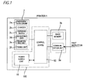
- FIG. 1 is a block diagram illustrating the electrical configuration of a printer 1 which is an example of an image forming apparatus.
- the printer 1 includes a printing unit 2, a communication unit 3a, an image memory 3b, and a power supply system 100.
- the power supply system 100 includes a power supply unit 10 and a control device 50.
- the power supply unit 10 acts as a power supply for the printer 1, and supplies electric power to the printing unit 2, the communication unit 3a, the image memory 3b, and the control device 50.
- the printing unit 2 includes a photosensitive drum 2a, a charger 2b for performing a charging process of charging the surface of the photosensitive drum 2a, an exposing device 2c for performing an exposing process of forming an electrostatic latent image on the surface of the photosensitive drum 2a, a developing unit 2d for performing a developing process of attaching a developer to the electrostatic latent image formed on the surface of the photosensitive drum 2a such that a developer image is formed, a transfer unit 2e for performing a transfer process of transferring the developer image onto a recording medium, and a fixing unit 2f for performing a fixing process of fixing the developer image transferred on the recording medium.
- the printing unit 2 performs a printing process of performing the charging process, the exposing process, the developing process, the transfer process, and the fixing process so as to print an image based on print data on a recording medium.
- the communication unit 3a performs communication with an information terminal device such as a PC, and has a function of receiving print instructions and print data from the information terminal device.
- the image memory 3b temporarily stores print data received from the information terminal device.
- the control device 50 controls the printing unit 2 such that the printing unit 2 performs the printing process of performing the charging process, the exposing process, the developing process, the transfer process, and the fixing process so as to print an image based on print data on a recording medium.
- the operating voltage of the printing unit 2 is generally 24V, whereas the operating voltages of the communication unit 3a, the image memory 3b, and the control device 50 are generally 3.3V.
- the printer 1 has a normal mode and a power saving mode, as operation modes.
- the normal mode is a mode in which the printer 1 is in a state in which the printer 1 can perform the printing process immediately in response to a print instruction or is performing the printing process. Therefore, in the normal mode, the power supply system 100 operates, and thus energization of the fixing unit 2f is controlled such that the fixing unit 2f is maintained at a temperature at which fixing is possible or a temperature slightly lower than the temperature at which fixing is possible.
- the power saving mode means a mode which the printer 1 enters if any print instruction is not received for a predetermined period, and in which the printer 1 is in a standby state. In the power saving mode, the power supply system 100 operates only partially, and thus the fixing unit 2f cannot be energized.
- the power supply system 100 includes the power supply unit 10 and the control device 50.
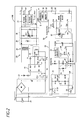
- the power supply unit 10 includes a switching power supply 20 and a low-capacity power supply circuit 30.
- the switching power supply 20 includes a rectifying/smoothing circuit 21, a control IC 22, a voltage generating circuit 23, a transformer 24, a field effect transistor (FET) Q1, a rectifying/smoothing circuit 25, a voltage detecting circuit 26, and DC to DC converters 27 and 28.
- a rectifying/smoothing circuit 21 includes a control IC 22, a voltage generating circuit 23, a transformer 24, a field effect transistor (FET) Q1, a rectifying/smoothing circuit 25, a voltage detecting circuit 26, and DC to DC converters 27 and 28.
- FET field effect transistor
- the switching power supply 20 rectifies and smoothes an AC voltage Vac of an AC power supply AC so as to generate DC voltages of +24V, +5V, and +3.3V.
- the DC voltage of +24V (hereinafter, referred to as DC 24V) is output from a first output terminal OUT1
- the DC voltage of +5V (hereinafter, referred to as DC 5V) is output from a second output terminal OUT2
- the DC voltage of +3.3V hereinafter, referred to as DC 3.3V
- the rectifying/smoothing circuit 21 is a so-called capacitor input type, and includes a photodiode for rectifying the AC voltage Vac (for example, 240V) of the AC power supply AC, and a capacitor for smoothing the rectified voltage. An output of the rectifying/smoothing circuit 21 is applied to a primary coil of the transformer 24.
- the transistor Q1 is an N-channel MOSFET, and is turned on or off in response to an on/off signal (PWM signal) given to the gate of the transistor Q1 by the control IC 22. Therefore, if the primary side of the transformer 24 oscillates, a voltage is induced at a secondary coil of the transformer 24.
- the voltage generating circuit 23 rectifies and smoothes a voltage induced at an auxiliary coil provided on the primary side of the transformer 24, thereby generating a power supply voltage Vcc for the control IC 22.
- the rectifying/smoothing circuit 25 rectifies and smoothes the voltage induced at the secondary coil of the transformer 24, thereby generating DC 24V.
- the voltage detecting circuit 26 includes a photocoupler PC1, and makes a light emitting diode LED1 of the photocoupler PC1 emit light in response to the detected level of the DC 24V output of the switching power supply 20.
- the photocoupler PC1 includes a phototransistor PT1 connected to a feedback port FB of the control IC 22. Therefore, a light signal of the light emitting diode LED1 is converted into an electric signal by the phototransistor PT1, and the detected value of the DC 24V output is fed back to the feedback port FB of the control IC 22.
- the DC to DC converter 27 converts DC 24V into DC 5V and outputs DC 5V
- the DC to DC converter 28 converts DC 24V into DC 3.3V and outputs DC 3.3V.
- the control IC 22 controls the on/off signal for the transistor Q1 in response to a control pulse signal Scp input to a control input port EN, such that oscillation of the primary side of the transformer 24 is controlled.
- the control IC 22 oscillates the primary side of the transformer 24 such that the DC voltages are generated, and in the power saving mode, the control IC 22 stops output of the on/off signal to the transistor Q1 such that oscillation of the primary side of the transformer 24 stops. In other words, in the power saving mode, the DC voltages of the switching power supply 20 are not output.
- the control pulse signal Scp is input from the control unit 50 to the control input port EN, and thus oscillation of the primary side of the transformer 24 starts in response to the control pulse signal Scp such that the DC voltages are output from the switching power supply 20.
- the switching power supply 20 becomes an output mode
- the switching power supply 20 becomes an output stop mode.
- a power supply voltage is supplied to an input port VH.
- the control device 50 includes an application-specific integrated circuit (ASIC) 51 and a switching power supply control unit 52.
- the ASIC 51 includes a main block B1 for controlling the printing unit 2 of the printer 1, and a mode control block B2 for mainly controlling the mode of the printer 1. A portion of the mode control may be performed by the main block B1.
- the main block B1 and the mode control block B2 are not necessarily configured by the ASIC 51.
- the main block B1 and the mode control block B2 may be configured by a main CPU and a sub CPU.
- a power supply port P1 of the main block B1 receives DC 3.3V from the DC to DC converter 28 of the switching power supply 20.
- the main block B1 can receive power supply to operate only in the normal mode. If the switching power supply 20 transitions to the output stop mode, that is, the power saving mode, the power supply to the main block B1 is cut off so as to stop the main block B1.
- the main block B1 includes a timer 55 and a memory 56, and detects the zero-crossing point ZP of the AC voltage Vac of the AC power supply AC (see FIG. 3 ) on the basis of a pulse signal Pzc input from a zero-crossing detecting circuit 34 to a port P5, as will be described below. Further, the main block B1 generates a zero-crossing signal Szc on the basis of the zero-crossing points ZP (see FIG. 3 ), and performs, for example, control on the energization of the fixing unit 2f, on the basis of the zero-crossing signal Szc.
- the timer 55 is used for time measurement during the detection of the zero-crossing points ZP.
- the memory 52 includes a ROM and a RAM.
- the ROM stores various programs to be executed by the ASIC 51, and the RAM stores various kinds of data when the programs are executed.
- a power supply port P2 of the mode control block B2 is connected to a DC-to-DC converter 33 of the low-capacity power supply circuit 30, and receives electric power from the low-capacity power supply circuit 30 in the normal mode and the power saving mode.
- the mode control block B2 switches the switching power supply 20 between the output mode and the output stop mode in which oscillation of the switching power supply 20 stops.
- the mode control block B2 outputs the control pulse signal Scp to the control IC 22, thereby switching the switching power supply 20 between the output mode and the output stop mode.
- the output mode is a mode in which the primary side of the transformer 24 is made oscillate such that the switching power supply 20 becomes an output state, and corresponds to the normal mode.
- the output stop mode is a mode in which the oscillation of the transformer 24 is stopped such that the output of the switching power supply 20 stops, and corresponds to the power saving mode.
- the control device 50 that is, the mode control block B2 of the ASIC 51 and a switching-power-supply operation control unit 52 receive power supply from the low-capacity power supply circuit 30.
- the switching power supply operation control unit 52 includes a light emitting diode LED2 of a photocoupler PC2 and a transistor Q2.
- the anode of the light emitting diode LED2 is connected to a power supply line of direct current +3.3V (hereinafter, referred to as DC 3.3VB) from the DC-to-DC converter 33.
- the light emitting diode LED2 constitutes a photocoupler PC2, together with a phototransistor PT2 connected to the control input port EN of the control IC 22 of the switching power supply 20. Therefore, if a control pulse signal Scp is output from a control port P3 of the mode control block B2 to the base of the transistor Q2, the control pulse signal Scp is optically transmitted through the photocoupler PC2, and is input to the control input port EN of the control IC 22.
- the control unit 50 specifically, the mode control block B2 of the ASIC 51 generates the control pulse signal Scp to restart oscillation of the switching power supply 20, and transmits the control pulse signal Scp to the switching power supply 20. Therefore, it is possible to appropriately perform switching from the power saving mode to the normal mode using electric power accumulated during the power saving mode. Also, the user can use a switch S1 to instruct the mode control block B2 to perform mode switching.
- a control signal Scon is output for turning on or off the DC to DC converter 28 of the switching power supply 20. For example, even in the normal mode, if electric power of DC 3.3VB supplied from the low-capacity power supply circuit 30 is sufficient, the AISC 51 stops the operation of the DC to DC converter 28 of the switching power supply 20 by the control signal Scon.
- the low-capacity power supply circuit 30 supplies electric power to the control unit 50 in the power saving mode and the normal mode. Specifically, in each mode, the low-capacity power supply circuit 30 supplies electric power to the mode control block B2 of the control unit 50 and the switching power supply operation control unit 52. In the normal mode, according to the amplitude of the AC voltage Vac, the low-capacity power supply circuit 30 supplies electric power from the AC power supply AC to the control device 50 or supplies electric power from DC 5V of the switching power supply 20 to the control device 50 through a diode D5. In the power saving mode, the low-capacity power supply circuit 30 supplies electric power from a smoothing capacitor C3 to the control device 50. Also, the low-capacity power supply circuit 30 includes a component for detecting the zero-crossing points of the AC power supply AC in the normal mode.
- the low-capacity power supply circuit 30 includes a first capacitor C1, a second capacitor C2, a rectifier circuit 31, a zener diode ZD1, the smoothing capacitor C3, the DC to DC converter 33, the pulse generating circuit 34 for zero-crossing detection, and an accumulating capacitor C4.
- the first capacitor C1 includes a first electrode C1p1 and a second electrode C1p2, the first electrode C1p1 is connected to one end of the AC power supply AC, and the second electrode C1p2 is connected to the rectifier circuit 31.
- the second capacitor C2 includes a first electrode C2p1 and a second electrode C2p2, the first electrode C2p1 is connected to the other end of the AC power supply AC, and the second electrode C2p2 is connected to the rectifier circuit 31.
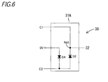
- the rectifier circuit 31 is electrically connected between the second electrode C1p2 of the first capacitor C1 and the second electrode of the second capacitor C2, and rectifies the AC voltage Vac applied to the first and second capacitors C1 and C2.
- the rectifier circuit 31 is configured by a bridge circuit composed of four diodes D1, D2, D3, and D4.
- the cathodes of the diode D1 and the diode D2 are connected at a first contact node Nd1, the anode of the diode D1 is connected to the second electrode C1p2 of the first capacitor C1, and the anode of the diode D2 is connected to the second electrode C2p2 of the second capacitor C2.
- the anodes of the diode D3 and the diode D4 are connected at a second contact node Nd2, the cathode of the diode D3 is connected to the second electrode C1p2 of the first capacitor C1, and the cathode of the diode D4 is connected to the second electrode C2p2 of the second capacitor C2.
- the second contact node Nd2 is connected to a reference potential line Lgd.
- the power supply system 100 is connected to a frame ground. Therefore, the reference potential line Lgd is also grounded such that the potential of the reference potential line Lgd is 0V.
- the smoothing capacitor C3 is connected to the rectifier circuit 31, and smoothes the rectified AC voltage so as to generate a smooth voltage Vch.
- the smoothing capacitor C3 is electrically connected to the DC 5V output terminal (second output terminal) OUT2 of the switching power supply 20 through the diode D5. For this reason, when electric power is supplied to the printer 1, the smoothing capacitor C3 and the accumulating capacitor C4 can be charged in a short time by DC 5V of the switching power supply 20.
- the diode D5 is for preventing a backward flow from the smoothing capacitor C3 to the DC to DC converter (27) side. Also, the zener diode ZD1 is for suppressing the smooth voltage Vch from rising in a case where the AC voltage Vac of the AC power supply AC rises.
- the DC to DC converter 33 converts the smooth voltage Vch into the DC voltage of +3.3VB.
- the DC 3.3VB is supplied to a switching-power-supply operation control unit 40 and the power supply port P2 of the mode control block B2.
- the mode control block B2 receives power supply from the low-capacity power supply circuit 30.
- the accumulating capacitor C4 is charged by DC 3.3VB from the DC to DC converter 33.
- the charged electric power is used for a drive current of the light emitting diode LED2 of the photocoupler PC2 during switching from the power saving mode to the normal mode. If the capacitances of the smoothing capacitor C3 and the accumulating capacitor C4 are appropriately selected, it is possible to accumulate an amount of electric power according to the needs for a predetermined voltage in the power saving mode.
- the smoothing capacitor C3 and the accumulating capacitor C4 capable of accumulating an amount of electric power to surely drive the light emitting diode LED2 of the photocoupler PC2 are used. Therefore, it is possible to reliably restart the switching power supply 20.
- the pulse generating circuit 34 for zero-crossing detection (hereinafter, referred to simply as a pulse generating circuit 34) is connected to a current path IP at the rear stage of the rectifier circuit 31, and detects the zero-crossing points ZP, that is, zero-crossings of the AC power supply AC on the basis of a rectified current Irc flowing in the current path IP.
- the pulse generating circuit 34 generates the pulse signal Pzc for zero-crossing detection (hereinafter, referred to simply as a pulse signal Pzc) corresponding to the zero-crossing points ZP, and the main block B1 of the ASIC 51 finally detects the zero-crossing points ZP on the basis of the pulse signal Pzc. Therefore, the pulse generating circuit 34 for zero-crossing detection and the main block B1 correspond to a zero-crossing detecting circuit.
- the pulse generating circuit 34 includes a resistor R1, a resistor R2, a diode D6, and an NPN transistor (hereinafter, referred to simply as a transistor) Q3.
- the current path IP is a path from the first contact node Nd1 of the rectifier circuit 31 to the reference potential line Lgd through the smoothing capacitor C3 and the resistor R1.
- the current path IP is a path in which an AC current Iac output from the AC power supply AC flows when the AC current Iac returns to the AC power supply AC.
- the transistor Q3 acts as a switching transistor which operates according to a base current generated by the rectified current Irc flowing in the current path IP. In other words, the transistor Q3 converts the rectified current Irc into the pulse signal Pzc.
- the collector of the transistor Q3 is connected to one end of the resistor R2, the base of the transistor Q3 is connected to the current path IP, and the emitter of the transistor Q3 is connected to the reference potential line Lgd.
- the resistor R2 is a pull-up resistor, and the other end of the resistor R2 is connected to the DC 3.3V output terminal OUT3 of the DC-to-DC converter 28.
- the transistor Q3 is turn on or off in response to the base current supplied to the base. Also, the pulse signal Pzc is output from the collector of the transistor Q3, is 0V when the transistor Q3 is in an ON state, and is 3.3V when the transistor Q3 is in an OFF state.
- the ASIC 51 detects the pulse period Tp of the pulse signal Pzc, and detects the zero-crossing points ZP of the AC voltage Vac of the AC power supply AC using the pulse period Tp (see FIG. 3 ).
- the transistor Q3 is not limited to a NPN transistor.
- the configuration for generating the pulse signal Pzc is not necessarily limited to the configuration of the transistor Q3 and the resistor R2.
- the transistor Q3 may be an FET.
- a voltage follower operational amplifier can be used as the current-to-voltage converter circuit.
- FIG. 3 shows waveforms in a case where the frequency of the AC power supply AC is 50 Hz, the AC voltage Vac is 240V (effective value), the capacitances of the capacitors C1 and C2 are 3300 pF (picofarads), the forward voltage drops of the diodes D1 to D4 are 0.6 V, a load current is 50 ⁇ A, and the zener voltage of the zener diode ZD1 is 8.2 V, the resistance of the resistor R1 is 15 k ⁇ , and the resistance of the resistor R2 is 10 k ⁇ .
- a path current Iip which is the total current of the rectified current Irc (the current flowing in the smoothing capacitor C3) and the zener diode ZD1 increases.
- the voltage drop of the resistor R1 that is, the voltage between the base and emitter of the transistor Q3 exceeds the turn-on voltage of the transistor Q3 due to the path current Iip, the transistor Q3 is turned on, and the pulse signal Pzc becomes 0V.
- the path current Iip further increases. Thereafter, if the path current Iip decreases and thus the voltage drop of the resistor R1 becomes equal to or lower than the turn-on voltage of the transistor Q3 at the timing t2, the pulse signal Pzc becomes about 3.3V.
- the timer 55 of the ASIC 51 starts to measure a period K1 in which the pulse signal Pzc is 0V (the timing t1 to the timing t2).
- the timer 55 starts to measure a period K2 in which the pulse signal Pzc is 3.3V (the timing t2 to the timing t3).
- the sum of the period K1 and the period K2, that is, a period from the time t1 to a timing t3 corresponds to the pulse period Tp of the pulse signal Pzc, and the timer 55 detects the pulse period Tp of the pulse signal Pzc.
- the ASIC 51 detects a zero-crossing point ZP1 on the basis of the pulse period Tp of the pulse signal Pzc.
- the pulse period Tp becomes 20 ms (milliseconds) which is the same as the period of the AC voltage Vac.
- the ASIC 51 calculates a timing t4 of the zero-crossing point ZP1 shown in FIG. 3 by the following Equation 1.
- t ⁇ 4 t ⁇ 3 + K ⁇ 1 / 2
- the ASIC 51 calculates a timing t6 of a zero-crossing point ZP2 shown in FIG. 5 by the following Equation 2.
- t ⁇ 6 t ⁇ 5 + K ⁇ 2 / 2
- the timings t1 and t3 of FIG. 3 are falling timings of the pulse signal Pzc, and the timings t2 and t5 of FIG. 3 are rising timings of the pulse signal Pzc. Therefore, it can be said that the ASIC 51 detects the zero-crossing points ZP on the basis of the rising timings and falling timings of the pulse signal Pzc.
- the ASIC 51 calculates timings t7 to t10 of zero-crossing points ZP3 to ZP6.
- the ASIC 51 generates the zero-crossing signal Szc which rises at the times t4, and t6 to t10 of the zero-crossing points ZP1 to ZP6, for example, and performs, for example, control on energization of the fixing unit 7, on the basis of the zero-crossing signal Szc.
- the pulse generating circuit 34 constituting the zero-crossing detecting circuit is provided in the low-capacity power supply circuit 30 which is used in the power saving mode, and the rectified current Irc of the low-capacity power supply circuit 30 is used to perform the zero-crossing detection.
- the rectified current Irc of the low-capacity power supply circuit 30 is significantly lower than the rectified current of the switching power supply 20. For this reason, the rectified current Irc flowing in the low-capacity power supply circuit 30 is used to perform the zero-crossing detection. Therefore, it is possible to perform zero-crossing detection capable of saving electric power.
- the amount of consumed electric power for the zero-crossing detection of the first embodiment is about 80 ⁇ W, which is significantly smaller than that of zero-crossing detection using a photocoupler according to the related art.
- the pulse generating circuit 34 (an example of a zero-crossing detecting circuit) is connected to the current path IP connecting the smoothing capacitor C3 and the reference potential line Lgd.
- This current path IP is necessary for generating the predetermined smooth voltage Vch. For this reason, it is possible to use an originally necessary path, without newly providing a current path dedicated for zero-crossing detection.
- FIG. 4 shows the configuration of a low-capacity power supply circuit 30A according to the second embodiment.
- the power supply system 100 of the second embodiment is different from the power supply system 100 of the first embodiment only in the current path on which the pulse generating circuit 34 is provided in the low-capacity power supply circuit. Therefore, this difference will be described, but the same components will not be described.
- the pulse generating circuit 34 (an example of the zero-crossing detecting circuit) is connected to a dedicated current path IPs dividing the rectified current Irc.
- the dedicated current path IPs is composed of two voltage dividing resistors R1 and R3 connected in series, and is disposed in parallel with the smoothing capacitor C3 between the rectifier circuit 31 and the smoothing capacitor C3.
- the pulse generating circuit 34 is connected between the two voltage dividing resistors R1 and R3.
- the base of the transistor Q3 of the pulse generating circuit 34 is connected between the two voltage dividing resistors R1 and R3. Then, the transistor Q3 is turned on or off according to a divided current Irc1 of the rectified current Irc, and zero-crossing detection is performed similarly to the first embodiment.
- a smoothing circuit 35 and the pulse generating circuit 34 for zero-crossing detection are separated from each other by a diode D7, and the zero-crossings are detected by a half-wave rectified voltage Vcha. Thereafter, the half-wave rectified voltage Vcha is smoothened to be a smooth voltage Vchb. Therefore, the smooth voltage is stabler as compared to the first embodiment, and thus +3.3VB generated by the DC-to-DC converter 33 is stabler.
- FIG. 5 shows the configuration of a low-capacity power supply circuit 30B according to the third embodiment.
- the power supply system 100 of the third embodiment is different from the power supply system 100 of the first embodiment only in the current path on which the pulse generating circuit 34 is provided in the low-capacity power supply circuit. Therefore, this difference will be described, but the same components will not be described.
- the pulse generating circuit 34 (an example of the zero-crossing detecting circuit) is connected to a dedicated current path IPs. Specifically, as shown in FIG. 5 , a resistor R4 is connected between the rectifier circuit 31 and the smoothing capacitor C3.
- the dedicated current path IPs is composed of a transistor Q4 (an example of a switch circuit) that is turned on or off according to the voltage drop of the resistor R4, and two voltage dividing resistors R1 and R3 connected between the transistor Q4 and the reference potential line Lgd.
- the pulse generating circuit 34 is connected between the two voltage dividing resistors R1 and R3. Specifically, the base of the transistor Q3 of the pulse generating circuit 34 is connected between the two voltage dividing resistors R1 and R3.
- the transistor Q4 is turned on, and zero-crossing detection is performed on the basis of a divided current Irc2 of the rectified current Irc. As described above, only when the rectified current Irc is equal to or larger than the predetermined current, the zero-crossing detection is performed. Therefore, the reliability of the zero-crossing detection is improved.
- the zener diode ZD1 and the smoothing capacitor C3 are provided.
- the present invention is not limited thereto. Any one of the zener diode ZD1 and the smoothing capacitor C3 may be provided. Even in this case, the zero-crossing detecting circuit 34 can detect the zero-crossing points of the AC power supply on the basis of the rectified current Irc flowing in the current path IP. Also, in a case where the smoothing capacitor C3 is provided, it is preferable to provide at least one of the resistor R1 and the diode D6.
- the zener diode ZD1 and the smoothing capacitor C3 may be omitted.
- the control device 50 in a case where the pulse signal (corresponding to a zero-crossing pulse) Pzc cannot be detected, the control device 50, specifically, the main block B1 of the ASIC 51 may determine that the voltage Vac of the AC power supply AC has dropped or the AC power supply AC has been suddenly turned off, and generate a power failure signal. This is because in the case where the pulse signal Pzc cannot be detected, it is possible to detect the voltage drop of the AC power supply AC or that the AC power supply AC is in an OFF state. In this case, it is possible to appropriately cope with occurrence of a power failure.
- the control device 50 in a case where the period K1 (corresponding to a pulse width) of the zero-crossing signal (corresponding to the zero-crossing pulse) Pzc is shorter than a predetermined period, the control device 50, specifically, the main block B1 of the ASIC 51 may determine that a rectangular wave has been input from the AC power supply AC, and generate a rectangular-wave power failure signal.
- the period K1 of the pulse signal Pzc becomes significantly short.
- the period K1 is compared to a predetermined period for detecting a rectangular wave, and if the period K1 is shorter than the predetermined period, it is possible to detect that a rectangular wave has been input from the AC power supply AC.
- the period K1 of the pulse signal Pzc it is possible to detect the zero-crossing points ZP on the basis of the period K1 of the pulse signal Pzc and to detect the waveform failure of the AC power supply AC. Therefore, it is possible to appropriately cope with the case where a rectangular wave has been input from the AC power supply.
- the smoothing capacitor C3 is connected to the DC 5V output terminal (OUT2) of the switching power supply 20 through the diode D5.
- this configuration is not necessary needed and thus may be omitted.
- the smoothing capacitor C3 may not be connected to the second output terminal OUT2 of the switching power supply 20.
- the zener diode ZD1 which is a constant voltage circuit is not necessarily needed, and thus may be omitted.
- the DC-to-DC converter 33 and the accumulating capacitor C4 are not necessarily needed, and thus may be omitted.
- the drive current of the light emitting diode LED2 of the photocoupler PC2 is supplied from the smoothing capacitor C3.
- the configuration of the rectifier circuit 31 is composed of the four diodes D1 to D4 shown in FIG. 2 or the like.
- the present invention is not limited thereto.
- the rectifier circuit 31 may be composed two diodes D2 and D4.
- the reference potential line Lgd is grounded.
- the present invention is not limited thereto. The present invention can be applied even to a case where reference potential line Lgd is not grounded.
- the power supply system 100 disclosed in this specification is applied to an image forming apparatus.
- the present invention is not limited thereto.
- the power supply system 100 can be applied to any apparatuses having a normal mode and a power saving mode.
Landscapes
- Engineering & Computer Science (AREA)
- Physics & Mathematics (AREA)
- General Physics & Mathematics (AREA)
- Microelectronics & Electronic Packaging (AREA)
- Power Engineering (AREA)
- Dc-Dc Converters (AREA)
- Power Conversion In General (AREA)
- Measurement Of Current Or Voltage (AREA)
- Direct Current Feeding And Distribution (AREA)
Applications Claiming Priority (1)
| Application Number | Priority Date | Filing Date | Title |
|---|---|---|---|
| JP2011241367A JP5780120B2 (ja) | 2011-11-02 | 2011-11-02 | 電源システム、同電源システムを備えた画像形成装置および小容量電源回路 |
Publications (3)
| Publication Number | Publication Date |
|---|---|
| EP2590308A2 true EP2590308A2 (de) | 2013-05-08 |
| EP2590308A3 EP2590308A3 (de) | 2014-05-14 |
| EP2590308B1 EP2590308B1 (de) | 2019-10-16 |
Family
ID=47257427
Family Applications (1)
| Application Number | Title | Priority Date | Filing Date |
|---|---|---|---|
| EP12186338.5A Active EP2590308B1 (de) | 2011-11-02 | 2012-09-27 | Stromversorgungssystem, Bilderzeugungsvorrichtung damit, und Netzteilschaltung mit niedriger Kapazität |
Country Status (4)
| Country | Link |
|---|---|
| US (1) | US9488944B2 (de) |
| EP (1) | EP2590308B1 (de) |
| JP (1) | JP5780120B2 (de) |
| CN (1) | CN103095160B (de) |
Families Citing this family (28)
| Publication number | Priority date | Publication date | Assignee | Title |
|---|---|---|---|---|
| JP5780120B2 (ja) | 2011-11-02 | 2015-09-16 | ブラザー工業株式会社 | 電源システム、同電源システムを備えた画像形成装置および小容量電源回路 |
| JP5834790B2 (ja) | 2011-11-09 | 2015-12-24 | ブラザー工業株式会社 | 電源システム、同電源システムを備えた画像形成装置および電源システムの制御方法 |
| JP2013110789A (ja) | 2011-11-17 | 2013-06-06 | Brother Ind Ltd | 電源システム、それを備えた画像形成装置、および小容量交流処理回路 |
| JP6056475B2 (ja) | 2012-12-28 | 2017-01-11 | ブラザー工業株式会社 | 電源システム、同電源システムを備えた画像形成装置 |
| JP6304577B2 (ja) | 2013-01-31 | 2018-04-04 | ブラザー工業株式会社 | 電源システム、同電源システムを備えた画像形成装置および電源システムの制御方法 |
| JP6111705B2 (ja) | 2013-02-01 | 2017-04-12 | ブラザー工業株式会社 | 電源システム |
| JP6020219B2 (ja) | 2013-02-06 | 2016-11-02 | ブラザー工業株式会社 | 電源システム |
| JP6044380B2 (ja) | 2013-02-18 | 2016-12-14 | ブラザー工業株式会社 | 電源システム、同電源システムを備えた画像形成装置 |
| JP6028653B2 (ja) * | 2013-03-27 | 2016-11-16 | ブラザー工業株式会社 | 電源システム、同電源システムを備えた画像形成装置 |
| JP5974952B2 (ja) * | 2013-03-27 | 2016-08-23 | ブラザー工業株式会社 | 電源システム、同電源システムを備えた画像形成装置 |
| JP6155801B2 (ja) | 2013-04-24 | 2017-07-05 | ブラザー工業株式会社 | 電源システムおよび画像形成装置 |
| JP6186858B2 (ja) | 2013-05-01 | 2017-08-30 | ブラザー工業株式会社 | 電源システムおよびインクジェット式画像形成装置 |
| JP6249741B2 (ja) | 2013-11-29 | 2017-12-20 | キヤノン株式会社 | 情報処理装置、及び情報処理装置の制御方法 |
| JP6269327B2 (ja) * | 2014-06-04 | 2018-01-31 | 株式会社リコー | 制御装置及び画像形成装置 |
| WO2016097476A1 (en) * | 2014-12-17 | 2016-06-23 | Salcomp Oyj | Switched-mode power supply |
| CA2985623C (en) | 2015-05-11 | 2024-03-05 | Stryker Corporation | System and method for driving an ultrasonic handpiece with a linear amplifier |
| CN106569015B (zh) * | 2015-10-13 | 2019-10-18 | 泰科电子(上海)有限公司 | 交流负载检测电路 |
| JP6066012B1 (ja) * | 2016-09-21 | 2017-01-25 | 富士ゼロックス株式会社 | 電力予測装置、画像形成装置、及び電力予測プログラム |
| WO2018205370A1 (zh) * | 2017-05-12 | 2018-11-15 | 厦门赛特勒磁电有限公司 | 电源转换模块 |
| JP6819527B2 (ja) * | 2017-09-22 | 2021-01-27 | ブラザー工業株式会社 | 検出装置及び工作機械 |
| JP7080098B2 (ja) * | 2018-04-24 | 2022-06-03 | エイブリック株式会社 | ゼロクロス検出回路およびセンサ装置 |
| KR20200029196A (ko) | 2018-09-10 | 2020-03-18 | 휴렛-팩커드 디벨롭먼트 컴퍼니, 엘.피. | 반파 교류전원의 제로크로스 정보를 출력하는 전원공급장치 |
| EP3648362B1 (de) * | 2018-11-02 | 2021-03-03 | Stmicroelectronics Sa | Verfahren zur beschränkung des über einen transponder empfangenen spannungsniveaus aus einem magnetfeld, und entsprechender transponder |
| JP7458843B2 (ja) * | 2020-03-23 | 2024-04-01 | 東芝テック株式会社 | 電力変換装置 |
| JP2022125765A (ja) * | 2021-02-17 | 2022-08-29 | キヤノン株式会社 | 画像形成装置 |
| JP7746691B2 (ja) | 2021-05-21 | 2025-10-01 | 富士電機株式会社 | 電源回路、電源装置 |
| TWI865097B (zh) * | 2023-06-01 | 2024-12-01 | 台達電子工業股份有限公司 | Led電源供應器 |
| CN119183229A (zh) | 2023-06-21 | 2024-12-24 | 台达电子工业股份有限公司 | Led电源供应器 |
Citations (1)
| Publication number | Priority date | Publication date | Assignee | Title |
|---|---|---|---|---|
| JP2010239774A (ja) | 2009-03-31 | 2010-10-21 | Brother Ind Ltd | ゼロクロス検出装置 |
Family Cites Families (42)
| Publication number | Priority date | Publication date | Assignee | Title |
|---|---|---|---|---|
| JPS55130543U (de) * | 1979-03-08 | 1980-09-16 | ||
| JPS55130543A (en) | 1979-03-29 | 1980-10-09 | Coulter Systems Corp | Image forming electronic photograph medium and formation of electric charge image |
| JPS6130774A (ja) * | 1984-07-24 | 1986-02-13 | Matsushita Electric Ind Co Ltd | ゼロボルト検出回路 |
| JPS6291265A (ja) | 1985-10-15 | 1987-04-25 | Nankai:Kk | シート素材の塗装装置 |
| JPS6291265U (de) * | 1985-11-26 | 1987-06-11 | ||
| US5166549A (en) * | 1991-08-07 | 1992-11-24 | General Electric Company | Zero-voltage crossing detector for soft-switching devices |
| US5914538A (en) | 1993-04-27 | 1999-06-22 | Canon Kabushiki Kaisha | Communication apparatus and power supply device therefor |
| JP3200258B2 (ja) | 1993-09-16 | 2001-08-20 | キヤノン株式会社 | 電源装置 |
| JPH07308065A (ja) * | 1994-05-10 | 1995-11-21 | Ricoh Co Ltd | 電源装置 |
| JPH0923638A (ja) | 1995-07-07 | 1997-01-21 | Ricoh Co Ltd | 電源装置 |
| DE19652604A1 (de) * | 1996-04-23 | 1997-10-30 | Thomson Brandt Gmbh | Netzteil für ein Gerät mit Standby-Betrieb |
| JP2000116027A (ja) * | 1998-03-10 | 2000-04-21 | Fiderikkusu:Kk | 電源装置 |
| US6320772B1 (en) * | 1999-05-26 | 2001-11-20 | Matsushita Electric Industrial Co., Ltd. | Converter circuit having control means with capability to short-circuit converter output |
| JP2001078446A (ja) | 1999-06-29 | 2001-03-23 | Toshiba Corp | 電源装置 |
| US6969959B2 (en) * | 2001-07-06 | 2005-11-29 | Lutron Electronics Co., Inc. | Electronic control systems and methods |
| CA2628211C (en) * | 2001-07-06 | 2014-09-16 | Lutron Electronics Company, Inc. | Electronic control systems and methods |
| JP2004056946A (ja) * | 2002-07-22 | 2004-02-19 | Shindengen Electric Mfg Co Ltd | スイッチング電源 |
| JP3922159B2 (ja) | 2002-10-30 | 2007-05-30 | ブラザー工業株式会社 | ヒータ駆動装置、定着装置および画像形成装置 |
| JP2004303469A (ja) | 2003-03-28 | 2004-10-28 | Brother Ind Ltd | 加熱装置及び画像形成装置 |
| JP4280244B2 (ja) * | 2005-02-15 | 2009-06-17 | シャープ株式会社 | ジョブ処理装置 |
| US20060209574A1 (en) * | 2005-03-17 | 2006-09-21 | Creative Technology, Ltd. | Power supply |
| CN2864700Y (zh) * | 2005-11-01 | 2007-01-31 | 海信集团有限公司 | 过零检测电路及采用过零检测电路的冰箱 |
| KR101235220B1 (ko) | 2006-07-28 | 2013-02-20 | 삼성전자주식회사 | 위상 감지 장치, 이를 구비한 위상 제어 장치 및 정착기제어 장치 |
| WO2009028053A1 (ja) | 2007-08-29 | 2009-03-05 | Mitsubishi Electric Corporation | 交流直流変換装置及びその装置を用いた圧縮機駆動装置並びに空気調和機 |
| CN201110615Y (zh) * | 2007-10-29 | 2008-09-03 | 珠海格力电器股份有限公司 | 空调控制器的过零信号检测电路及一种空调 |
| EP2104401B1 (de) * | 2008-03-17 | 2013-08-14 | Universal Lighting Technologies, Inc. | Nulldurchgangserkennung von Leitungsspannung/-strom unterschiedlicher Amplitude |
| CN101265916B (zh) * | 2008-05-12 | 2011-08-31 | 中南大学 | 电风扇的调速控制系统和方法 |
| KR101497062B1 (ko) | 2008-07-25 | 2015-03-05 | 페어차일드코리아반도체 주식회사 | 스위치 제어 장치, 스위치 제어 방법, 및 이를 이용하는 컨버터 |
| JP2010054306A (ja) * | 2008-08-27 | 2010-03-11 | Sharp Corp | ゼロクロス検知回路、及びそのゼロクロス検知回路を含む画像形成装置 |
| JP5056835B2 (ja) * | 2009-11-26 | 2012-10-24 | ブラザー工業株式会社 | 加熱装置および画像形成装置 |
| WO2011070512A2 (en) * | 2009-12-07 | 2011-06-16 | Coppergate Communications Ltd. | Enhanced power supply unit for powerline networks |
| JP2011199976A (ja) | 2010-03-18 | 2011-10-06 | Panasonic Corp | 電源装置 |
| JP5780812B2 (ja) | 2010-05-12 | 2015-09-16 | キヤノン株式会社 | 電圧検知装置及び像加熱装置 |
| WO2012099551A1 (en) * | 2011-01-21 | 2012-07-26 | Hulusi Bulent Ertan | Power-level waveform generation method |
| JP5684064B2 (ja) * | 2011-07-28 | 2015-03-11 | ブラザー工業株式会社 | ゼロクロス検出回路および同検出回路を備えた画像形成装置 |
| JP5752513B2 (ja) | 2011-07-29 | 2015-07-22 | ブラザー工業株式会社 | 電源システム、それを備えた画像形成装置 |
| JP5561255B2 (ja) | 2011-08-09 | 2014-07-30 | ブラザー工業株式会社 | 交流電圧検出回路および同検出回路を備えた画像形成装置 |
| JP5780120B2 (ja) | 2011-11-02 | 2015-09-16 | ブラザー工業株式会社 | 電源システム、同電源システムを備えた画像形成装置および小容量電源回路 |
| JP5834790B2 (ja) | 2011-11-09 | 2015-12-24 | ブラザー工業株式会社 | 電源システム、同電源システムを備えた画像形成装置および電源システムの制御方法 |
| JP2013110789A (ja) | 2011-11-17 | 2013-06-06 | Brother Ind Ltd | 電源システム、それを備えた画像形成装置、および小容量交流処理回路 |
| JP6304577B2 (ja) | 2013-01-31 | 2018-04-04 | ブラザー工業株式会社 | 電源システム、同電源システムを備えた画像形成装置および電源システムの制御方法 |
| JP6044380B2 (ja) | 2013-02-18 | 2016-12-14 | ブラザー工業株式会社 | 電源システム、同電源システムを備えた画像形成装置 |
-
2011
- 2011-11-02 JP JP2011241367A patent/JP5780120B2/ja active Active
-
2012
- 2012-09-26 CN CN201210364448.2A patent/CN103095160B/zh active Active
- 2012-09-27 EP EP12186338.5A patent/EP2590308B1/de active Active
- 2012-09-27 US US13/629,545 patent/US9488944B2/en active Active
Patent Citations (1)
| Publication number | Priority date | Publication date | Assignee | Title |
|---|---|---|---|---|
| JP2010239774A (ja) | 2009-03-31 | 2010-10-21 | Brother Ind Ltd | ゼロクロス検出装置 |
Also Published As
| Publication number | Publication date |
|---|---|
| CN103095160A (zh) | 2013-05-08 |
| US9488944B2 (en) | 2016-11-08 |
| JP2013096902A (ja) | 2013-05-20 |
| EP2590308A3 (de) | 2014-05-14 |
| CN103095160B (zh) | 2016-08-03 |
| US20130111237A1 (en) | 2013-05-02 |
| EP2590308B1 (de) | 2019-10-16 |
| JP5780120B2 (ja) | 2015-09-16 |
Similar Documents
| Publication | Publication Date | Title |
|---|---|---|
| EP2590308A2 (de) | Stromversorgungssystem, Bilderzeugungsvorrichtung damit, und Netzteilschaltung mit niedriger Kapazität | |
| EP2595292B1 (de) | Stromversorgungssystem, Bilderzeugungsvorrichtung damit, und AC-Verarbeitungsschaltung mit niedriger Kapazität | |
| EP2552004B1 (de) | Netzteil mit Hilfsversorgung des Steuergeräts im Energiesparmodus | |
| EP2551681B1 (de) | Nulldurchgangsdetektor und Bilderzeugungsvorrichtung damit | |
| US9537419B2 (en) | Power supply system and image forming apparatus having the same | |
| KR101403203B1 (ko) | 스위칭 전원 장치 및 스위칭 전원 장치를 갖는 화상 형성 장치 | |
| JP5873293B2 (ja) | 電源装置および画像形成装置 | |
| US10277764B2 (en) | Power supply apparatus and image forming apparatus | |
| JP5974952B2 (ja) | 電源システム、同電源システムを備えた画像形成装置 | |
| JP6075827B2 (ja) | スイッチング電源装置及び画像形成装置 | |
| EP2450750A2 (de) | Stromversorgungssystem und Bilderzeugungsvorrichtung | |
| JP6028653B2 (ja) | 電源システム、同電源システムを備えた画像形成装置 | |
| US20140293659A1 (en) | High-voltage generating apparatus, high-voltage power supply, and image forming apparatus | |
| JP6364894B2 (ja) | 電源システムおよび画像形成装置 | |
| JP2020072610A (ja) | 電源装置及び画像形成装置 | |
| US20050219864A1 (en) | Power source apparatus | |
| KR200173056Y1 (ko) | 모니터의 전원공급회로 | |
| JP2007330081A (ja) | スイッチング電源装置 | |
| KR20000007290U (ko) | 모니터의 전압 크기 표시회로 | |
| KR19990034334A (ko) | 모니터의 스위칭 전원회로에 있어서 소프트 스타트회로 |
Legal Events
| Date | Code | Title | Description |
|---|---|---|---|
| PUAI | Public reference made under article 153(3) epc to a published international application that has entered the european phase |
Free format text: ORIGINAL CODE: 0009012 |
|
| AK | Designated contracting states |
Kind code of ref document: A2 Designated state(s): AL AT BE BG CH CY CZ DE DK EE ES FI FR GB GR HR HU IE IS IT LI LT LU LV MC MK MT NL NO PL PT RO RS SE SI SK SM TR |
|
| AX | Request for extension of the european patent |
Extension state: BA ME |
|
| PUAL | Search report despatched |
Free format text: ORIGINAL CODE: 0009013 |
|
| AK | Designated contracting states |
Kind code of ref document: A3 Designated state(s): AL AT BE BG CH CY CZ DE DK EE ES FI FR GB GR HR HU IE IS IT LI LT LU LV MC MK MT NL NO PL PT RO RS SE SI SK SM TR |
|
| AX | Request for extension of the european patent |
Extension state: BA ME |
|
| RIC1 | Information provided on ipc code assigned before grant |
Ipc: H02M 7/00 20060101AFI20140410BHEP Ipc: H02M 1/00 20070101ALI20140410BHEP Ipc: G01R 19/175 20060101ALI20140410BHEP |
|
| 17P | Request for examination filed |
Effective date: 20141114 |
|
| RBV | Designated contracting states (corrected) |
Designated state(s): AL AT BE BG CH CY CZ DE DK EE ES FI FR GB GR HR HU IE IS IT LI LT LU LV MC MK MT NL NO PL PT RO RS SE SI SK SM TR |
|
| STAA | Information on the status of an ep patent application or granted ep patent |
Free format text: STATUS: EXAMINATION IS IN PROGRESS |
|
| 17Q | First examination report despatched |
Effective date: 20161215 |
|
| GRAP | Despatch of communication of intention to grant a patent |
Free format text: ORIGINAL CODE: EPIDOSNIGR1 |
|
| STAA | Information on the status of an ep patent application or granted ep patent |
Free format text: STATUS: GRANT OF PATENT IS INTENDED |
|
| INTG | Intention to grant announced |
Effective date: 20190520 |
|
| GRAS | Grant fee paid |
Free format text: ORIGINAL CODE: EPIDOSNIGR3 |
|
| GRAA | (expected) grant |
Free format text: ORIGINAL CODE: 0009210 |
|
| STAA | Information on the status of an ep patent application or granted ep patent |
Free format text: STATUS: THE PATENT HAS BEEN GRANTED |
|
| AK | Designated contracting states |
Kind code of ref document: B1 Designated state(s): AL AT BE BG CH CY CZ DE DK EE ES FI FR GB GR HR HU IE IS IT LI LT LU LV MC MK MT NL NO PL PT RO RS SE SI SK SM TR |
|
| REG | Reference to a national code |
Ref country code: GB Ref legal event code: FG4D |
|
| REG | Reference to a national code |
Ref country code: CH Ref legal event code: EP |
|
| REG | Reference to a national code |
Ref country code: DE Ref legal event code: R096 Ref document number: 602012064857 Country of ref document: DE |
|
| REG | Reference to a national code |
Ref country code: IE Ref legal event code: FG4D |
|
| REG | Reference to a national code |
Ref country code: AT Ref legal event code: REF Ref document number: 1192269 Country of ref document: AT Kind code of ref document: T Effective date: 20191115 |
|
| REG | Reference to a national code |
Ref country code: NL Ref legal event code: MP Effective date: 20191016 |
|
| REG | Reference to a national code |
Ref country code: LT Ref legal event code: MG4D |
|
| REG | Reference to a national code |
Ref country code: AT Ref legal event code: MK05 Ref document number: 1192269 Country of ref document: AT Kind code of ref document: T Effective date: 20191016 |
|
| PG25 | Lapsed in a contracting state [announced via postgrant information from national office to epo] |
Ref country code: LV Free format text: LAPSE BECAUSE OF FAILURE TO SUBMIT A TRANSLATION OF THE DESCRIPTION OR TO PAY THE FEE WITHIN THE PRESCRIBED TIME-LIMIT Effective date: 20191016 Ref country code: LT Free format text: LAPSE BECAUSE OF FAILURE TO SUBMIT A TRANSLATION OF THE DESCRIPTION OR TO PAY THE FEE WITHIN THE PRESCRIBED TIME-LIMIT Effective date: 20191016 Ref country code: SE Free format text: LAPSE BECAUSE OF FAILURE TO SUBMIT A TRANSLATION OF THE DESCRIPTION OR TO PAY THE FEE WITHIN THE PRESCRIBED TIME-LIMIT Effective date: 20191016 Ref country code: NL Free format text: LAPSE BECAUSE OF FAILURE TO SUBMIT A TRANSLATION OF THE DESCRIPTION OR TO PAY THE FEE WITHIN THE PRESCRIBED TIME-LIMIT Effective date: 20191016 Ref country code: ES Free format text: LAPSE BECAUSE OF FAILURE TO SUBMIT A TRANSLATION OF THE DESCRIPTION OR TO PAY THE FEE WITHIN THE PRESCRIBED TIME-LIMIT Effective date: 20191016 Ref country code: GR Free format text: LAPSE BECAUSE OF FAILURE TO SUBMIT A TRANSLATION OF THE DESCRIPTION OR TO PAY THE FEE WITHIN THE PRESCRIBED TIME-LIMIT Effective date: 20200117 Ref country code: PL Free format text: LAPSE BECAUSE OF FAILURE TO SUBMIT A TRANSLATION OF THE DESCRIPTION OR TO PAY THE FEE WITHIN THE PRESCRIBED TIME-LIMIT Effective date: 20191016 Ref country code: NO Free format text: LAPSE BECAUSE OF FAILURE TO SUBMIT A TRANSLATION OF THE DESCRIPTION OR TO PAY THE FEE WITHIN THE PRESCRIBED TIME-LIMIT Effective date: 20200116 Ref country code: PT Free format text: LAPSE BECAUSE OF FAILURE TO SUBMIT A TRANSLATION OF THE DESCRIPTION OR TO PAY THE FEE WITHIN THE PRESCRIBED TIME-LIMIT Effective date: 20200217 Ref country code: BG Free format text: LAPSE BECAUSE OF FAILURE TO SUBMIT A TRANSLATION OF THE DESCRIPTION OR TO PAY THE FEE WITHIN THE PRESCRIBED TIME-LIMIT Effective date: 20200116 Ref country code: FI Free format text: LAPSE BECAUSE OF FAILURE TO SUBMIT A TRANSLATION OF THE DESCRIPTION OR TO PAY THE FEE WITHIN THE PRESCRIBED TIME-LIMIT Effective date: 20191016 Ref country code: AT Free format text: LAPSE BECAUSE OF FAILURE TO SUBMIT A TRANSLATION OF THE DESCRIPTION OR TO PAY THE FEE WITHIN THE PRESCRIBED TIME-LIMIT Effective date: 20191016 |
|
| PG25 | Lapsed in a contracting state [announced via postgrant information from national office to epo] |
Ref country code: HR Free format text: LAPSE BECAUSE OF FAILURE TO SUBMIT A TRANSLATION OF THE DESCRIPTION OR TO PAY THE FEE WITHIN THE PRESCRIBED TIME-LIMIT Effective date: 20191016 Ref country code: RS Free format text: LAPSE BECAUSE OF FAILURE TO SUBMIT A TRANSLATION OF THE DESCRIPTION OR TO PAY THE FEE WITHIN THE PRESCRIBED TIME-LIMIT Effective date: 20191016 Ref country code: IS Free format text: LAPSE BECAUSE OF FAILURE TO SUBMIT A TRANSLATION OF THE DESCRIPTION OR TO PAY THE FEE WITHIN THE PRESCRIBED TIME-LIMIT Effective date: 20200224 |
|
| PG25 | Lapsed in a contracting state [announced via postgrant information from national office to epo] |
Ref country code: AL Free format text: LAPSE BECAUSE OF FAILURE TO SUBMIT A TRANSLATION OF THE DESCRIPTION OR TO PAY THE FEE WITHIN THE PRESCRIBED TIME-LIMIT Effective date: 20191016 |
|
| REG | Reference to a national code |
Ref country code: DE Ref legal event code: R097 Ref document number: 602012064857 Country of ref document: DE |
|
| PG2D | Information on lapse in contracting state deleted |
Ref country code: IS |
|
| PG25 | Lapsed in a contracting state [announced via postgrant information from national office to epo] |
Ref country code: CZ Free format text: LAPSE BECAUSE OF FAILURE TO SUBMIT A TRANSLATION OF THE DESCRIPTION OR TO PAY THE FEE WITHIN THE PRESCRIBED TIME-LIMIT Effective date: 20191016 Ref country code: RO Free format text: LAPSE BECAUSE OF FAILURE TO SUBMIT A TRANSLATION OF THE DESCRIPTION OR TO PAY THE FEE WITHIN THE PRESCRIBED TIME-LIMIT Effective date: 20191016 Ref country code: DK Free format text: LAPSE BECAUSE OF FAILURE TO SUBMIT A TRANSLATION OF THE DESCRIPTION OR TO PAY THE FEE WITHIN THE PRESCRIBED TIME-LIMIT Effective date: 20191016 Ref country code: EE Free format text: LAPSE BECAUSE OF FAILURE TO SUBMIT A TRANSLATION OF THE DESCRIPTION OR TO PAY THE FEE WITHIN THE PRESCRIBED TIME-LIMIT Effective date: 20191016 Ref country code: IS Free format text: LAPSE BECAUSE OF FAILURE TO SUBMIT A TRANSLATION OF THE DESCRIPTION OR TO PAY THE FEE WITHIN THE PRESCRIBED TIME-LIMIT Effective date: 20200216 |
|
| PLBE | No opposition filed within time limit |
Free format text: ORIGINAL CODE: 0009261 |
|
| STAA | Information on the status of an ep patent application or granted ep patent |
Free format text: STATUS: NO OPPOSITION FILED WITHIN TIME LIMIT |
|
| PG25 | Lapsed in a contracting state [announced via postgrant information from national office to epo] |
Ref country code: IT Free format text: LAPSE BECAUSE OF FAILURE TO SUBMIT A TRANSLATION OF THE DESCRIPTION OR TO PAY THE FEE WITHIN THE PRESCRIBED TIME-LIMIT Effective date: 20191016 Ref country code: SK Free format text: LAPSE BECAUSE OF FAILURE TO SUBMIT A TRANSLATION OF THE DESCRIPTION OR TO PAY THE FEE WITHIN THE PRESCRIBED TIME-LIMIT Effective date: 20191016 Ref country code: SM Free format text: LAPSE BECAUSE OF FAILURE TO SUBMIT A TRANSLATION OF THE DESCRIPTION OR TO PAY THE FEE WITHIN THE PRESCRIBED TIME-LIMIT Effective date: 20191016 |
|
| 26N | No opposition filed |
Effective date: 20200717 |
|
| PG25 | Lapsed in a contracting state [announced via postgrant information from national office to epo] |
Ref country code: SI Free format text: LAPSE BECAUSE OF FAILURE TO SUBMIT A TRANSLATION OF THE DESCRIPTION OR TO PAY THE FEE WITHIN THE PRESCRIBED TIME-LIMIT Effective date: 20191016 |
|
| PG25 | Lapsed in a contracting state [announced via postgrant information from national office to epo] |
Ref country code: MC Free format text: LAPSE BECAUSE OF FAILURE TO SUBMIT A TRANSLATION OF THE DESCRIPTION OR TO PAY THE FEE WITHIN THE PRESCRIBED TIME-LIMIT Effective date: 20191016 |
|
| REG | Reference to a national code |
Ref country code: CH Ref legal event code: PL |
|
| REG | Reference to a national code |
Ref country code: BE Ref legal event code: MM Effective date: 20200930 |
|
| PG25 | Lapsed in a contracting state [announced via postgrant information from national office to epo] |
Ref country code: LU Free format text: LAPSE BECAUSE OF NON-PAYMENT OF DUE FEES Effective date: 20200927 |
|
| PG25 | Lapsed in a contracting state [announced via postgrant information from national office to epo] |
Ref country code: BE Free format text: LAPSE BECAUSE OF NON-PAYMENT OF DUE FEES Effective date: 20200930 Ref country code: CH Free format text: LAPSE BECAUSE OF NON-PAYMENT OF DUE FEES Effective date: 20200930 Ref country code: LI Free format text: LAPSE BECAUSE OF NON-PAYMENT OF DUE FEES Effective date: 20200930 Ref country code: IE Free format text: LAPSE BECAUSE OF NON-PAYMENT OF DUE FEES Effective date: 20200927 |
|
| PG25 | Lapsed in a contracting state [announced via postgrant information from national office to epo] |
Ref country code: TR Free format text: LAPSE BECAUSE OF FAILURE TO SUBMIT A TRANSLATION OF THE DESCRIPTION OR TO PAY THE FEE WITHIN THE PRESCRIBED TIME-LIMIT Effective date: 20191016 Ref country code: MT Free format text: LAPSE BECAUSE OF FAILURE TO SUBMIT A TRANSLATION OF THE DESCRIPTION OR TO PAY THE FEE WITHIN THE PRESCRIBED TIME-LIMIT Effective date: 20191016 Ref country code: CY Free format text: LAPSE BECAUSE OF FAILURE TO SUBMIT A TRANSLATION OF THE DESCRIPTION OR TO PAY THE FEE WITHIN THE PRESCRIBED TIME-LIMIT Effective date: 20191016 |
|
| PG25 | Lapsed in a contracting state [announced via postgrant information from national office to epo] |
Ref country code: MK Free format text: LAPSE BECAUSE OF FAILURE TO SUBMIT A TRANSLATION OF THE DESCRIPTION OR TO PAY THE FEE WITHIN THE PRESCRIBED TIME-LIMIT Effective date: 20191016 |
|
| P01 | Opt-out of the competence of the unified patent court (upc) registered |
Effective date: 20230529 |
|
| PGFP | Annual fee paid to national office [announced via postgrant information from national office to epo] |
Ref country code: DE Payment date: 20250805 Year of fee payment: 14 |
|
| PGFP | Annual fee paid to national office [announced via postgrant information from national office to epo] |
Ref country code: GB Payment date: 20250807 Year of fee payment: 14 |
|
| PGFP | Annual fee paid to national office [announced via postgrant information from national office to epo] |
Ref country code: FR Payment date: 20250808 Year of fee payment: 14 |