EP2592173A2 - Agencement et procédé de réalisation d'un procédé ALD à basse température - Google Patents
Agencement et procédé de réalisation d'un procédé ALD à basse température Download PDFInfo
- Publication number
- EP2592173A2 EP2592173A2 EP12191796.7A EP12191796A EP2592173A2 EP 2592173 A2 EP2592173 A2 EP 2592173A2 EP 12191796 A EP12191796 A EP 12191796A EP 2592173 A2 EP2592173 A2 EP 2592173A2
- Authority
- EP
- European Patent Office
- Prior art keywords
- vacuum
- substrate
- coating chamber
- vacuum coating
- deposition chamber
- Prior art date
- Legal status (The legal status is an assumption and is not a legal conclusion. Google has not performed a legal analysis and makes no representation as to the accuracy of the status listed.)
- Withdrawn
Links
- 238000000034 method Methods 0.000 title claims abstract description 45
- 239000000758 substrate Substances 0.000 claims abstract description 94
- 238000001771 vacuum deposition Methods 0.000 claims abstract description 71
- 239000002243 precursor Substances 0.000 claims abstract description 24
- 238000010438 heat treatment Methods 0.000 claims abstract description 14
- 239000000463 material Substances 0.000 claims description 18
- 238000011010 flushing procedure Methods 0.000 claims description 4
- 230000001681 protective effect Effects 0.000 claims description 4
- 238000004519 manufacturing process Methods 0.000 abstract description 3
- 238000000151 deposition Methods 0.000 abstract 2
- 230000008021 deposition Effects 0.000 abstract 2
- 238000005137 deposition process Methods 0.000 abstract 1
- 238000000231 atomic layer deposition Methods 0.000 description 25
- 239000010408 film Substances 0.000 description 12
- 239000007789 gas Substances 0.000 description 12
- 238000000576 coating method Methods 0.000 description 7
- 239000011248 coating agent Substances 0.000 description 5
- 239000002184 metal Substances 0.000 description 3
- 239000004033 plastic Substances 0.000 description 3
- 229920003023 plastic Polymers 0.000 description 3
- 239000011888 foil Substances 0.000 description 2
- 239000002985 plastic film Substances 0.000 description 2
- 229920006255 plastic film Polymers 0.000 description 2
- 238000009423 ventilation Methods 0.000 description 2
- 238000000137 annealing Methods 0.000 description 1
- 238000001311 chemical methods and process Methods 0.000 description 1
- 238000010924 continuous production Methods 0.000 description 1
- 238000009826 distribution Methods 0.000 description 1
- 238000010327 methods by industry Methods 0.000 description 1
- 230000005855 radiation Effects 0.000 description 1
- 239000000126 substance Substances 0.000 description 1
- 238000007669 thermal treatment Methods 0.000 description 1
- 239000010409 thin film Substances 0.000 description 1
- 230000001960 triggered effect Effects 0.000 description 1
- 238000013022 venting Methods 0.000 description 1
Images

Classifications
-
- C—CHEMISTRY; METALLURGY
- C23—COATING METALLIC MATERIAL; COATING MATERIAL WITH METALLIC MATERIAL; CHEMICAL SURFACE TREATMENT; DIFFUSION TREATMENT OF METALLIC MATERIAL; COATING BY VACUUM EVAPORATION, BY SPUTTERING, BY ION IMPLANTATION OR BY CHEMICAL VAPOUR DEPOSITION, IN GENERAL; INHIBITING CORROSION OF METALLIC MATERIAL OR INCRUSTATION IN GENERAL
- C23C—COATING METALLIC MATERIAL; COATING MATERIAL WITH METALLIC MATERIAL; SURFACE TREATMENT OF METALLIC MATERIAL BY DIFFUSION INTO THE SURFACE, BY CHEMICAL CONVERSION OR SUBSTITUTION; COATING BY VACUUM EVAPORATION, BY SPUTTERING, BY ION IMPLANTATION OR BY CHEMICAL VAPOUR DEPOSITION, IN GENERAL
- C23C16/00—Chemical coating by decomposition of gaseous compounds, without leaving reaction products of surface material in the coating, i.e. chemical vapour deposition [CVD] processes
- C23C16/44—Chemical coating by decomposition of gaseous compounds, without leaving reaction products of surface material in the coating, i.e. chemical vapour deposition [CVD] processes characterised by the method of coating
- C23C16/455—Chemical coating by decomposition of gaseous compounds, without leaving reaction products of surface material in the coating, i.e. chemical vapour deposition [CVD] processes characterised by the method of coating characterised by the method used for introducing gases into reaction chamber or for modifying gas flows in reaction chamber
- C23C16/45523—Pulsed gas flow or change of composition over time
- C23C16/45525—Atomic layer deposition [ALD]
-
- C—CHEMISTRY; METALLURGY
- C23—COATING METALLIC MATERIAL; COATING MATERIAL WITH METALLIC MATERIAL; CHEMICAL SURFACE TREATMENT; DIFFUSION TREATMENT OF METALLIC MATERIAL; COATING BY VACUUM EVAPORATION, BY SPUTTERING, BY ION IMPLANTATION OR BY CHEMICAL VAPOUR DEPOSITION, IN GENERAL; INHIBITING CORROSION OF METALLIC MATERIAL OR INCRUSTATION IN GENERAL
- C23C—COATING METALLIC MATERIAL; COATING MATERIAL WITH METALLIC MATERIAL; SURFACE TREATMENT OF METALLIC MATERIAL BY DIFFUSION INTO THE SURFACE, BY CHEMICAL CONVERSION OR SUBSTITUTION; COATING BY VACUUM EVAPORATION, BY SPUTTERING, BY ION IMPLANTATION OR BY CHEMICAL VAPOUR DEPOSITION, IN GENERAL
- C23C16/00—Chemical coating by decomposition of gaseous compounds, without leaving reaction products of surface material in the coating, i.e. chemical vapour deposition [CVD] processes
- C23C16/44—Chemical coating by decomposition of gaseous compounds, without leaving reaction products of surface material in the coating, i.e. chemical vapour deposition [CVD] processes characterised by the method of coating
- C23C16/4401—Means for minimising impurities, e.g. dust, moisture or residual gas, in the reaction chamber
- C23C16/4409—Means for minimising impurities, e.g. dust, moisture or residual gas, in the reaction chamber characterised by sealing means
-
- C—CHEMISTRY; METALLURGY
- C23—COATING METALLIC MATERIAL; COATING MATERIAL WITH METALLIC MATERIAL; CHEMICAL SURFACE TREATMENT; DIFFUSION TREATMENT OF METALLIC MATERIAL; COATING BY VACUUM EVAPORATION, BY SPUTTERING, BY ION IMPLANTATION OR BY CHEMICAL VAPOUR DEPOSITION, IN GENERAL; INHIBITING CORROSION OF METALLIC MATERIAL OR INCRUSTATION IN GENERAL
- C23C—COATING METALLIC MATERIAL; COATING MATERIAL WITH METALLIC MATERIAL; SURFACE TREATMENT OF METALLIC MATERIAL BY DIFFUSION INTO THE SURFACE, BY CHEMICAL CONVERSION OR SUBSTITUTION; COATING BY VACUUM EVAPORATION, BY SPUTTERING, BY ION IMPLANTATION OR BY CHEMICAL VAPOUR DEPOSITION, IN GENERAL
- C23C16/00—Chemical coating by decomposition of gaseous compounds, without leaving reaction products of surface material in the coating, i.e. chemical vapour deposition [CVD] processes
- C23C16/44—Chemical coating by decomposition of gaseous compounds, without leaving reaction products of surface material in the coating, i.e. chemical vapour deposition [CVD] processes characterised by the method of coating
- C23C16/458—Chemical coating by decomposition of gaseous compounds, without leaving reaction products of surface material in the coating, i.e. chemical vapour deposition [CVD] processes characterised by the method of coating characterised by the method used for supporting substrates in the reaction chamber
- C23C16/4582—Rigid and flat substrates, e.g. plates or discs
- C23C16/4583—Rigid and flat substrates, e.g. plates or discs the substrate being supported substantially horizontally
-
- C—CHEMISTRY; METALLURGY
- C23—COATING METALLIC MATERIAL; COATING MATERIAL WITH METALLIC MATERIAL; CHEMICAL SURFACE TREATMENT; DIFFUSION TREATMENT OF METALLIC MATERIAL; COATING BY VACUUM EVAPORATION, BY SPUTTERING, BY ION IMPLANTATION OR BY CHEMICAL VAPOUR DEPOSITION, IN GENERAL; INHIBITING CORROSION OF METALLIC MATERIAL OR INCRUSTATION IN GENERAL
- C23C—COATING METALLIC MATERIAL; COATING MATERIAL WITH METALLIC MATERIAL; SURFACE TREATMENT OF METALLIC MATERIAL BY DIFFUSION INTO THE SURFACE, BY CHEMICAL CONVERSION OR SUBSTITUTION; COATING BY VACUUM EVAPORATION, BY SPUTTERING, BY ION IMPLANTATION OR BY CHEMICAL VAPOUR DEPOSITION, IN GENERAL
- C23C16/00—Chemical coating by decomposition of gaseous compounds, without leaving reaction products of surface material in the coating, i.e. chemical vapour deposition [CVD] processes
- C23C16/44—Chemical coating by decomposition of gaseous compounds, without leaving reaction products of surface material in the coating, i.e. chemical vapour deposition [CVD] processes characterised by the method of coating
- C23C16/46—Chemical coating by decomposition of gaseous compounds, without leaving reaction products of surface material in the coating, i.e. chemical vapour deposition [CVD] processes characterised by the method of coating characterised by the method used for heating the substrate
-
- C—CHEMISTRY; METALLURGY
- C23—COATING METALLIC MATERIAL; COATING MATERIAL WITH METALLIC MATERIAL; CHEMICAL SURFACE TREATMENT; DIFFUSION TREATMENT OF METALLIC MATERIAL; COATING BY VACUUM EVAPORATION, BY SPUTTERING, BY ION IMPLANTATION OR BY CHEMICAL VAPOUR DEPOSITION, IN GENERAL; INHIBITING CORROSION OF METALLIC MATERIAL OR INCRUSTATION IN GENERAL
- C23C—COATING METALLIC MATERIAL; COATING MATERIAL WITH METALLIC MATERIAL; SURFACE TREATMENT OF METALLIC MATERIAL BY DIFFUSION INTO THE SURFACE, BY CHEMICAL CONVERSION OR SUBSTITUTION; COATING BY VACUUM EVAPORATION, BY SPUTTERING, BY ION IMPLANTATION OR BY CHEMICAL VAPOUR DEPOSITION, IN GENERAL
- C23C16/00—Chemical coating by decomposition of gaseous compounds, without leaving reaction products of surface material in the coating, i.e. chemical vapour deposition [CVD] processes
- C23C16/44—Chemical coating by decomposition of gaseous compounds, without leaving reaction products of surface material in the coating, i.e. chemical vapour deposition [CVD] processes characterised by the method of coating
- C23C16/48—Chemical coating by decomposition of gaseous compounds, without leaving reaction products of surface material in the coating, i.e. chemical vapour deposition [CVD] processes characterised by the method of coating by irradiation, e.g. photolysis, radiolysis, particle radiation
- C23C16/482—Chemical coating by decomposition of gaseous compounds, without leaving reaction products of surface material in the coating, i.e. chemical vapour deposition [CVD] processes characterised by the method of coating by irradiation, e.g. photolysis, radiolysis, particle radiation using incoherent light, UV to IR, e.g. lamps
-
- C—CHEMISTRY; METALLURGY
- C23—COATING METALLIC MATERIAL; COATING MATERIAL WITH METALLIC MATERIAL; CHEMICAL SURFACE TREATMENT; DIFFUSION TREATMENT OF METALLIC MATERIAL; COATING BY VACUUM EVAPORATION, BY SPUTTERING, BY ION IMPLANTATION OR BY CHEMICAL VAPOUR DEPOSITION, IN GENERAL; INHIBITING CORROSION OF METALLIC MATERIAL OR INCRUSTATION IN GENERAL
- C23C—COATING METALLIC MATERIAL; COATING MATERIAL WITH METALLIC MATERIAL; SURFACE TREATMENT OF METALLIC MATERIAL BY DIFFUSION INTO THE SURFACE, BY CHEMICAL CONVERSION OR SUBSTITUTION; COATING BY VACUUM EVAPORATION, BY SPUTTERING, BY ION IMPLANTATION OR BY CHEMICAL VAPOUR DEPOSITION, IN GENERAL
- C23C16/00—Chemical coating by decomposition of gaseous compounds, without leaving reaction products of surface material in the coating, i.e. chemical vapour deposition [CVD] processes
- C23C16/44—Chemical coating by decomposition of gaseous compounds, without leaving reaction products of surface material in the coating, i.e. chemical vapour deposition [CVD] processes characterised by the method of coating
- C23C16/54—Apparatus specially adapted for continuous coating
- C23C16/545—Apparatus specially adapted for continuous coating for coating elongated substrates
Definitions
- the invention relates to an arrangement and a method for carrying out a low-temperature ALD process for producing material films on flat substrates in an evacuable vacuum coating chamber, which is provided with an inlet for a precursor gas and a heater for heating the substrate.
- Such substrates may be plastic films, metal foils, etc. coated on one side with one or more atomic layers of materials by means of one or more successive ALD processes (ALD: Atomic Layer Deposition).
- ALD Atomic Layer Deposition
- An ALD process is characterized in that first of all different precursor gases are introduced into the vacuum coating chamber and deposited on the substrate. Precursors are precursor substances. The desired material films on the substrate are subsequently produced by a chemical process, which is supported / triggered thermally and / or plasmachemically.
- the additional application of heat due to the ALD process is necessary for process engineering reasons and is generally realized by means of radiation or contact heating systems installed in a vacuum or in a separate chamber. It is also known to carry out a subsequent thermal treatment of the applied film of material by means of flash lamps.
- the heating is usually dimensioned so that the temperature of the substrate to be coated is stabilized throughout the entire process.
- a coating by means of an ALD process is not or only partially possible due to the necessary process temperatures.
- the invention is based on the object of providing an arrangement and a method for carrying out a low-temperature ALD process for producing material films on flat temperature-sensitive substrates, wherein in particular it is to be ensured that their temperature does not appreciably increase during the ALD process.
- the object underlying the invention is achieved in that the vacuum coating chamber is designed to be open at the bottom and covered by a vacuum-tight flashlight box with a flash lamp panel as a heater and that the vacuum coating chamber from below with a lifting table for receiving a band-shaped substrate is vacuum-tight closed.
- slot-shaped openings are provided as passages for passing the band-shaped substrate over the lifting table between the lower edge of the vacuum coating chamber and the lifting table.
- the belt-shaped substrate is fed from a supply roll to a take-up roll through the vacuum coating chamber, the rolls being outside the vacuum coating chamber are arranged.
- the slot-shaped openings are also formed as inlets for the precursor gas.
- the object underlying the invention is further achieved in that the vacuum coating chamber is covered at the top by a vacuum tight fitted flash lamp box with a flash lamp panel as a heater and that the vacuum coating chamber is sealed vacuum-tight in the lower part with a receptacle for individual substrates.
- the receptacle for the individual substrates may be formed as a plate or consist of individual supports, pins, etc.
- a protective window is arranged between the flash lamp box and the substrate in the case of both vacuum coating chambers according to the invention.
- the substrate can also be slit several times.
- the flash of the substrate is made during or after each process step.
- the substrate is slit during the admission of the second precursor gas into the vacuum coating chamber or during the second rinsing process.
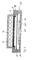
- the low-temperature ALD device consists of a vacuum deposition chamber 1 (process chamber) open in the drawing, which is covered at the top by a vacuum-tightly fitted flash lamp box 2 with a flash lamp panel 3 and a window 4.
- the window 4 in the flash lamp box 2 is vacuum-tightly inserted into the vacuum chamber 1 by means of seals 5.
- the flashlamp field 3 replaces the otherwise required in ALD processes heating.
- Below the flash lamp box 2 is located in the vacuum coating chamber 1, an optional protective window 6 for the protection of unwanted deposits in the area of the flash lamp box. 2
- a belt-shaped substrate 7 is guided over a vertically movable lift table 8 which simultaneously serves to close the vacuum coating chamber 1 during the ALD process, whereby slot-shaped openings 9 for the belt-shaped substrate 7 are kept free.
- band-shaped substrates 7 are for example plastic or metal foils or other thin films into consideration.
- the vacuum coating chamber 1 is provided with at least one inlet / outlet 10 for precursor gas, as well as with a connection, not shown, for a vacuum pump.
- the lifting table 8 is lowered slightly to release the belt-shaped substrate 7, so that it can then be transported through the slot-shaped openings 8 on. This can be done from a supply roll 11 to a take-up roll 12, which are located outside of the vacuum coating chamber 1.
- FIG. 1 shown ALD device including the roll-to-roll arrangement 11, 12 for the band-shaped substrate 7 completely enveloped by a further vacuum chamber 13.
- the band-shaped substrate 7 can be moved continuously or stepwise through the slit-shaped openings 9 (without lifting table function), since only in the heat-irradiated area does a reaction of the applied precursors take place.
- the precursor gases are pumped equally or exclusively through one of the slot-shaped openings 9.
- FIG. 2 illustrated ALD device with flash assist is provided for the low temperature ALD coating of thin single substrates 14.
- a flash lamp box 2 In the direction of the upper area of the vacuum coating chamber 15 is also a flash lamp box 2 with a flash lamp panel 3, which replaces the otherwise required in ALD processes heating.
- window 4 Below the flash lamp box 2 is window 4, which is vacuum-tightly inserted into the vacuum coating chamber 15 via seals 5.
- the individual substrates 14 are here in the vacuum coating chamber 15 on a receptacle 16 in the form of a plate or individual supports 17, pins, etc. arranged.
- the lower part (bottom part) of the vacuum coating chamber 15 may be detachably connected thereto and, for example, as part of a lift table 8 as in FIG Fig. 1 be educated.
- the supply of precursor gas takes place here via an inlet / outlet 10.
- the ALD device after Fig. 2 is particularly suitable for thin single substrates 14 made of plastic, metal or other materials. Should the individual substrates 14 on Supports 17 or pins are to be stored in the vacuum coating chamber 15, so they must have a sufficient inherent rigidity, otherwise the individual substrates 14 must be supported by a plate or other support means.
- a port 19 for a vacuum pump may be disposed in the lower portion of the vacuum deposition chamber 15 below the single substrate 14 or at another suitable location.
- the substrate heating is replaced by a high-energy pulse-like heat application in the vacuum chamber in an ALD process of the type mentioned, which is characterized by extremely short turn-on of the flash lamp field 3.
- ALD process of the type mentioned, which is characterized by extremely short turn-on of the flash lamp field 3.
- This can be done with the flash lamp field 3 with adjustable flash energy, for example with a FLA process (FLA: Flash Lamp Annealing).
- the energy to be introduced locally into the layer must be dimensioned such that the distribution of the heat occurring as a result of heat conduction in the substrate 7, 14 only leads to a slight heating thereof, which should be in the region of room temperature. Consequently, it is necessary to work with the shortest possible turn-on times of the flash lamp field, at the same time the flash energy can be controlled accordingly to a short-term heating of the the substrate 7, 14 applied material film to reach the required reaction temperature of the precursors.
- Room temperature should be understood to mean a temperature which is around 20 ° C.
- the substrate 7, 14 can also be flashed several times with the shortest possible turn-on time of the flash lamp field 3, whereby the flashes of the substrates 7, 14 can take place during or after each process step.
- the belt-shaped substrate 7 can be transported further, if necessary after a slight lowering of the lifting table 8.
- a prior venting of the vacuum coating chamber 1 may be omitted if this and the roll-to-roll system 11, 12 is surrounded by a vacuum chamber 13.
- the vacuum coating chamber 15 must first be aerated, after which the coated single substrate 14 can be removed after opening the vacuum coating chamber 15.
- the execution could also Fig. 2 are also enveloped by a vacuum chamber 11 and in this a magazine system for storing the individual substrates 14, for transport in and out of the vacuum coating chamber 15, and for storing coated individual substrates 14 are arranged.
Landscapes
- Chemical & Material Sciences (AREA)
- General Chemical & Material Sciences (AREA)
- Chemical Kinetics & Catalysis (AREA)
- Engineering & Computer Science (AREA)
- Materials Engineering (AREA)
- Mechanical Engineering (AREA)
- Metallurgy (AREA)
- Organic Chemistry (AREA)
- Health & Medical Sciences (AREA)
- Toxicology (AREA)
- Physical Vapour Deposition (AREA)
Applications Claiming Priority (1)
| Application Number | Priority Date | Filing Date | Title |
|---|---|---|---|
| DE102011085914 | 2011-11-08 |
Publications (2)
| Publication Number | Publication Date |
|---|---|
| EP2592173A2 true EP2592173A2 (fr) | 2013-05-15 |
| EP2592173A3 EP2592173A3 (fr) | 2014-03-05 |
Family
ID=47257471
Family Applications (1)
| Application Number | Title | Priority Date | Filing Date |
|---|---|---|---|
| EP12191796.7A Withdrawn EP2592173A3 (fr) | 2011-11-08 | 2012-11-08 | Agencement et procédé de réalisation d'un procédé ALD à basse température |
Country Status (1)
| Country | Link |
|---|---|
| EP (1) | EP2592173A3 (fr) |
Cited By (2)
| Publication number | Priority date | Publication date | Assignee | Title |
|---|---|---|---|---|
| WO2016102749A1 (fr) * | 2014-12-22 | 2016-06-30 | Picosun Oy | Procédé et appareil de dépôt de couche atomique comprenant une source de photons |
| CN106086822A (zh) * | 2016-07-28 | 2016-11-09 | 河北大学 | 适于批处理的卷对卷真空镀膜反应装置 |
Family Cites Families (7)
| Publication number | Priority date | Publication date | Assignee | Title |
|---|---|---|---|---|
| JP2006294750A (ja) * | 2005-04-07 | 2006-10-26 | Toshiba Corp | 薄膜堆積装置及び方法 |
| EP1790758A1 (fr) * | 2005-11-25 | 2007-05-30 | Interuniversitair Microelektronica Centrum ( Imec) | Procédé de dépot de couches atomiques (ALD ) pour produire une couche de haute qualité |
| US20100024732A1 (en) * | 2006-06-02 | 2010-02-04 | Nima Mokhlesi | Systems for Flash Heating in Atomic Layer Deposition |
| JP2008027932A (ja) * | 2006-07-18 | 2008-02-07 | Sony Corp | 半導体装置の製造方法および原子層蒸着装置 |
| US20080175993A1 (en) * | 2006-10-13 | 2008-07-24 | Jalal Ashjaee | Reel-to-reel reaction of a precursor film to form solar cell absorber |
| FI123539B (fi) * | 2009-02-09 | 2013-06-28 | Beneq Oy | ALD-reaktori, menetelmä ALD-reaktorin lataamiseksi ja tuotantolinja |
| JP5423808B2 (ja) * | 2009-12-11 | 2014-02-19 | 富士電機株式会社 | 可撓性基板の搬送装置 |
-
2012
- 2012-11-08 EP EP12191796.7A patent/EP2592173A3/fr not_active Withdrawn
Non-Patent Citations (1)
| Title |
|---|
| None |
Cited By (8)
| Publication number | Priority date | Publication date | Assignee | Title |
|---|---|---|---|---|
| WO2016102749A1 (fr) * | 2014-12-22 | 2016-06-30 | Picosun Oy | Procédé et appareil de dépôt de couche atomique comprenant une source de photons |
| CN107109646A (zh) * | 2014-12-22 | 2017-08-29 | 皮考逊公司 | Ald 方法和包括光子源的设备 |
| RU2704875C2 (ru) * | 2014-12-22 | 2019-10-31 | Пикосан Ой | Устройство и способ атомно-слоевого осаждения покрытия на поверхность подложки |
| TWI676705B (zh) * | 2014-12-22 | 2019-11-11 | 芬蘭商皮寇桑公司 | 沉積技術(二) |
| US10597778B2 (en) | 2014-12-22 | 2020-03-24 | Picosun Oy | ALD method and apparatus including a photon source |
| CN107109646B (zh) * | 2014-12-22 | 2022-03-18 | 皮考逊公司 | Ald方法和包括光子源的设备 |
| CN106086822A (zh) * | 2016-07-28 | 2016-11-09 | 河北大学 | 适于批处理的卷对卷真空镀膜反应装置 |
| CN106086822B (zh) * | 2016-07-28 | 2018-06-08 | 河北大学 | 适于批处理的卷对卷真空镀膜反应装置 |
Also Published As
| Publication number | Publication date |
|---|---|
| EP2592173A3 (fr) | 2014-03-05 |
Similar Documents
| Publication | Publication Date | Title |
|---|---|---|
| DE60310291T2 (de) | Verfahren und Vorrichtung zur Gasphasenbeschichtung | |
| EP2144296B2 (fr) | Procédé de fabrication d'une couche semi-conductrice | |
| EP2536865B1 (fr) | Dispositif de revêtement ainsi que procédé pour le fonctionnement d'un dispositif de revêtement doté d'une plaque de protection | |
| DE3051188C2 (fr) | ||
| DE69011052T2 (de) | Chemische Gasphasen-Beschichtungsanlage der In-Line-Bauart. | |
| DE69032189T2 (de) | Peripherieabdichtung für Halbleiterplättchen und verfahren zu deren Verwendung | |
| EP2291868B1 (fr) | Dispositif et procédé de régulation de température d'objets dans une chambre de traitement | |
| DE3317349C2 (fr) | ||
| DE60038669T2 (de) | Wärmebehandlungsgerät und methode | |
| DE102014117228B4 (de) | Backvorrichtung für einen Wafer, der mit einer ein Lösungsmittel enthaltenden Beschichtung beschichtet ist | |
| DE1646153A1 (de) | UEberzugsverfahren und Vorrichtung hierzu | |
| WO2010060646A1 (fr) | Procédé de fabrication de couches semi-conductrices ou de substrats revêtus, traités par du sélénium et/ou du soufre élémentaire, en particulier de substrats bidimensionnels | |
| EP2870625B1 (fr) | Installation et procédé destinés à traiter des substrats | |
| EP2870623B1 (fr) | Boîtier de processus, agencement et procédé de traitement d'un substrat revêtu | |
| EP3610050B1 (fr) | Dispositif de revêtement et procédés permettant le dépôt réactif en phase vapeur sous vide sur un substrat | |
| DE19716707A1 (de) | Halbleiterkristallscheiben -Wärmebehandlungsvorrichtung | |
| DE102009011496A1 (de) | Verfahren und Vorrichtung zur thermischen Umsetzung metallischer Precursorschichten in halbleitende Schichten mit Chalkogenrückgewinnung | |
| DE102006047472A1 (de) | Verfahren und Vorrichtung zur oberflächennahen Behandlung von flächigen Substraten | |
| EP2609619B1 (fr) | Dispositif et procédé de traitement de tranches | |
| DE69111540T2 (de) | Vorrichtung zum Herstellen einer Schicht im Vacuum. | |
| DE3889735T2 (de) | Chemischer dampfniederschlagsreaktor und dessen verwendung. | |
| DE102017215662B4 (de) | Filmbildungsvorrichtung und filmbildungsverfahren | |
| DE102009009022A1 (de) | Verfahren und Vorrichtung zur Beschichtung von flachen Substraten mit Chalkogenen | |
| DE19813523C2 (de) | CVD-Reaktor und dessen Verwendung | |
| EP3411513B1 (fr) | Procédé de dépôt d'une couche cdte sur un substrat |
Legal Events
| Date | Code | Title | Description |
|---|---|---|---|
| PUAI | Public reference made under article 153(3) epc to a published international application that has entered the european phase |
Free format text: ORIGINAL CODE: 0009012 |
|
| AK | Designated contracting states |
Kind code of ref document: A2 Designated state(s): AL AT BE BG CH CY CZ DE DK EE ES FI FR GB GR HR HU IE IS IT LI LT LU LV MC MK MT NL NO PL PT RO RS SE SI SK SM TR |
|
| AX | Request for extension of the european patent |
Extension state: BA ME |
|
| PUAL | Search report despatched |
Free format text: ORIGINAL CODE: 0009013 |
|
| AK | Designated contracting states |
Kind code of ref document: A3 Designated state(s): AL AT BE BG CH CY CZ DE DK EE ES FI FR GB GR HR HU IE IS IT LI LT LU LV MC MK MT NL NO PL PT RO RS SE SI SK SM TR |
|
| AX | Request for extension of the european patent |
Extension state: BA ME |
|
| RIC1 | Information provided on ipc code assigned before grant |
Ipc: C23C 16/54 20060101ALI20140127BHEP Ipc: C23C 16/458 20060101ALI20140127BHEP Ipc: C23C 16/48 20060101ALI20140127BHEP Ipc: C23C 16/44 20060101ALI20140127BHEP Ipc: C23C 16/455 20060101ALI20140127BHEP Ipc: C23C 16/46 20060101AFI20140127BHEP |
|
| 17P | Request for examination filed |
Effective date: 20140814 |
|
| RBV | Designated contracting states (corrected) |
Designated state(s): AL AT BE BG CH CY CZ DE DK EE ES FI FR GB GR HR HU IE IS IT LI LT LU LV MC MK MT NL NO PL PT RO RS SE SI SK SM TR |
|
| STAA | Information on the status of an ep patent application or granted ep patent |
Free format text: STATUS: THE APPLICATION HAS BEEN WITHDRAWN |
|
| 18W | Application withdrawn |
Effective date: 20180205 |