EP2592644A2 - Appareil de traitement à plasma - Google Patents
Appareil de traitement à plasma Download PDFInfo
- Publication number
- EP2592644A2 EP2592644A2 EP12181447.9A EP12181447A EP2592644A2 EP 2592644 A2 EP2592644 A2 EP 2592644A2 EP 12181447 A EP12181447 A EP 12181447A EP 2592644 A2 EP2592644 A2 EP 2592644A2
- Authority
- EP
- European Patent Office
- Prior art keywords
- antenna
- plasma
- high frequency
- interval
- openings
- Prior art date
- Legal status (The legal status is an assumption and is not a legal conclusion. Google has not performed a legal analysis and makes no representation as to the accuracy of the status listed.)
- Withdrawn
Links
Images




Classifications
-
- H—ELECTRICITY
- H05—ELECTRIC TECHNIQUES NOT OTHERWISE PROVIDED FOR
- H05H—PLASMA TECHNIQUE; PRODUCTION OF ACCELERATED ELECTRICALLY-CHARGED PARTICLES OR OF NEUTRONS; PRODUCTION OR ACCELERATION OF NEUTRAL MOLECULAR OR ATOMIC BEAMS
- H05H1/00—Generating plasma; Handling plasma
- H05H1/24—Generating plasma
- H05H1/46—Generating plasma using applied electromagnetic fields, e.g. high frequency or microwave energy
-
- H—ELECTRICITY
- H01—ELECTRIC ELEMENTS
- H01J—ELECTRIC DISCHARGE TUBES OR DISCHARGE LAMPS
- H01J37/00—Discharge tubes with provision for introducing objects or material to be exposed to the discharge, e.g. for the purpose of examination or processing thereof
- H01J37/32—Gas-filled discharge tubes
- H01J37/32009—Arrangements for generation of plasma specially adapted for examination or treatment of objects, e.g. plasma sources
- H01J37/32082—Radio frequency generated discharge
- H01J37/321—Radio frequency generated discharge the radio frequency energy being inductively coupled to the plasma
- H01J37/3211—Antennas, e.g. particular shapes of coils
-
- C—CHEMISTRY; METALLURGY
- C23—COATING METALLIC MATERIAL; COATING MATERIAL WITH METALLIC MATERIAL; CHEMICAL SURFACE TREATMENT; DIFFUSION TREATMENT OF METALLIC MATERIAL; COATING BY VACUUM EVAPORATION, BY SPUTTERING, BY ION IMPLANTATION OR BY CHEMICAL VAPOUR DEPOSITION, IN GENERAL; INHIBITING CORROSION OF METALLIC MATERIAL OR INCRUSTATION IN GENERAL
- C23C—COATING METALLIC MATERIAL; COATING MATERIAL WITH METALLIC MATERIAL; SURFACE TREATMENT OF METALLIC MATERIAL BY DIFFUSION INTO THE SURFACE, BY CHEMICAL CONVERSION OR SUBSTITUTION; COATING BY VACUUM EVAPORATION, BY SPUTTERING, BY ION IMPLANTATION OR BY CHEMICAL VAPOUR DEPOSITION, IN GENERAL
- C23C16/00—Chemical coating by decomposition of gaseous compounds, without leaving reaction products of surface material in the coating, i.e. chemical vapour deposition [CVD] processes
- C23C16/44—Chemical coating by decomposition of gaseous compounds, without leaving reaction products of surface material in the coating, i.e. chemical vapour deposition [CVD] processes characterised by the method of coating
- C23C16/50—Chemical coating by decomposition of gaseous compounds, without leaving reaction products of surface material in the coating, i.e. chemical vapour deposition [CVD] processes characterised by the method of coating using electric discharges
- C23C16/505—Chemical coating by decomposition of gaseous compounds, without leaving reaction products of surface material in the coating, i.e. chemical vapour deposition [CVD] processes characterised by the method of coating using electric discharges using radio frequency discharges
- C23C16/507—Chemical coating by decomposition of gaseous compounds, without leaving reaction products of surface material in the coating, i.e. chemical vapour deposition [CVD] processes characterised by the method of coating using electric discharges using radio frequency discharges using external electrodes, e.g. in tunnel type reactors
-
- H—ELECTRICITY
- H10—SEMICONDUCTOR DEVICES; ELECTRIC SOLID-STATE DEVICES NOT OTHERWISE PROVIDED FOR
- H10P—GENERIC PROCESSES OR APPARATUS FOR THE MANUFACTURE OR TREATMENT OF DEVICES COVERED BY CLASS H10
- H10P50/00—Etching of wafers, substrates or parts of devices
- H10P50/20—Dry etching; Plasma etching; Reactive-ion etching
- H10P50/24—Dry etching; Plasma etching; Reactive-ion etching of semiconductor materials
- H10P50/242—Dry etching; Plasma etching; Reactive-ion etching of semiconductor materials of Group IV materials
-
- C—CHEMISTRY; METALLURGY
- C23—COATING METALLIC MATERIAL; COATING MATERIAL WITH METALLIC MATERIAL; CHEMICAL SURFACE TREATMENT; DIFFUSION TREATMENT OF METALLIC MATERIAL; COATING BY VACUUM EVAPORATION, BY SPUTTERING, BY ION IMPLANTATION OR BY CHEMICAL VAPOUR DEPOSITION, IN GENERAL; INHIBITING CORROSION OF METALLIC MATERIAL OR INCRUSTATION IN GENERAL
- C23C—COATING METALLIC MATERIAL; COATING MATERIAL WITH METALLIC MATERIAL; SURFACE TREATMENT OF METALLIC MATERIAL BY DIFFUSION INTO THE SURFACE, BY CHEMICAL CONVERSION OR SUBSTITUTION; COATING BY VACUUM EVAPORATION, BY SPUTTERING, BY ION IMPLANTATION OR BY CHEMICAL VAPOUR DEPOSITION, IN GENERAL
- C23C16/00—Chemical coating by decomposition of gaseous compounds, without leaving reaction products of surface material in the coating, i.e. chemical vapour deposition [CVD] processes
- C23C16/22—Chemical coating by decomposition of gaseous compounds, without leaving reaction products of surface material in the coating, i.e. chemical vapour deposition [CVD] processes characterised by the deposition of inorganic material, other than metallic material
- C23C16/30—Deposition of compounds, mixtures or solid solutions, e.g. borides, carbides, nitrides
- C23C16/40—Oxides
- C23C16/401—Oxides containing silicon
- C23C16/402—Silicon dioxide
Definitions
- the present invention relates to a plasma processing apparatus, and more particularly, to an inductively-coupled-plasma (ICP) type plasma processing apparatus.
- ICP inductively-coupled-plasma
- Plasma processing apparatuses using high frequency (HF) to generate plasma can be classified into capacitively-coupled-plasma (CCP) type plasma processing apparatuses capable of generating capacitively-coupled plasma and inductively-coupled-plasma type (ICP) plasma processing apparatuses capable of generating inductively-coupled plasma.
- CCP capacitively-coupled-plasma
- ICP inductively-coupled-plasma type
- ICP type plasma processing apparatuses an induction electric field generated by applying a radiofrequency current to flow to an antenna is used to generate plasma.
- the ICP plasma processing apparatuses have the advantage of being capable to lower the plasma potential.
- a flat-board-like antenna is mounted on an opening of a vacuum container through an insulating frame.
- a high frequency power supply is supplied to the flat-board-like antenna so that a high frequency current can flow from one end to the other end of the antenna, and thereby plasma is generated due to the induced electric field. It has been described in WO 2009/142016 that the plasma is used to perform a plasma treatment to the substrate in the plasma processing apparatus.
- the antenna has to be long and the impedance (particularly inductance) of the antenna increases for a large substrate; thus, a large potential difference between the two terminals of the antenna would be induced.
- the antenna potential is influenced by the plasma potential via the capacitance of the plasma, the antenna potential is increased with an increase of the plasma potential.
- the plasma generating action of CCP and the plasma generating action of original ICP may be superimposed in order to increase the amplitude of voltage of the antenna located around the higher voltage terminal, the plasma density located around the higher voltage terminal may become higher than the plasma density of other places. As a result, the uniformity of the plasma density distribution in the longitudinal direction of the antenna may deteriorate, and consequently the uniformity of the substrate treatment may get worse.
- one exemplary embodiment of the present invention is to provide an (inductively-coupled plasma) ICP type plasma processing apparatus capable of decreasing the effective inductance of the antenna and suppressing the potential difference generated between the two ends of each side in the longitudinal direction of the antenna, and moreover capable of not only decreasing the plasma potential, but also increasing uniformity of the plasma density distribution in the longitudinal direction of the antenna.
- the plasma processing apparatus of the present invention is an ICP type.
- the plasma processing apparatus includes an antenna, substantially straight in a plan view of the antenna, wherein a plasma is generated for performing a plasma treatment to a substrate by applying a high frequency current to the antenna to induce an electric field in a vacuum container.
- the antenna includes two rectangular conductor plates disposed on a same plane along a surface of the substrate in a manner that the two rectangular conductor plates are parallel to each other with an interval therebetween. An end of a side in a longitudinal direction of each of the two rectangular conductor plates is connected through a conductor so as to form a go-and-return conductor, wherein the high frequency current flows in the two rectangular conductor plates in opposite directions.
- a plurality of notches are formed at the sides of the two rectangular conductor plates adjacent to the interval, and the notches of the plurality of notches facing each other define an opening.
- the plurality of notches forms the plurality of openings, and the plurality of openings are separately arranged in the longitudinal direction of the antenna.
- the effective inductance of the antenna is decreased due to the mutual inductance existing between the go-and-return conductors. Accordingly, the potential difference generated between the two ends of each side in the longitudinal direction of the antenna can be decreased, thus not only the plasma potential can be decreased, but also the uniformity of the plasma density distribution in the longitudinal direction of the antenna can be improved.
- the high frequency current has a tendency to flow to the ends of the two rectangular conductor plates by the skin effect.
- the inductance also impedance, hereinafter the same
- the inductance is smaller. Accordingly, more high frequency current may flow along the sides adjacent to the interval and the openings which are formed thereon.
- the openings are separately arranged in the longitudinal direction of the antenna and having the function similar to coil and simple structure, the openings can be formed like a plurality of coils connected in series. Accordingly in such simple structure, a strong magnetic field may be generated around each of the openings and success rate of plasma generating can be increased.
- the inductance of the antenna can be decreased and the potential difference generated between the two ends of the antenna in the longitudinal direction can also be decreased. The effect is as described above.
- the openings of the plurality of openings located at the two ends of the antenna in the longitudinal direction can be formed larger than the rest of the plurality of openings.
- the distance between each of the plurality of openings located at two ends of the antenna in the longitudinal direction is smaller than a distance between the rest of two openings of the plurality of openings. Combination of both can also be used.
- the two rectangular conductor plates are configured in a V-shape cross-sectional structure, wherein the V-shape cross-sectional structure is separated relatively wide at a side facing away from the surface of the substrate and the two sides of the two rectangular plates adjacent to the interval are closely disposed in parallel to each other with the interval therebetween.
- the two rectangular conductor plates are configured in a manner that the two rectangular conductor plates are bent in a short side direction to form a U-shape cross-sectional structure, wherein the U-shape cross-sectional structure is separated relatively wide at a side facing away from the surface of the substrate and the two sides of the two rectangular plates adjacent to the interval are closely disposed in parallel to each other with the interval therebetween.
- a periphery of a side facing away from the interval of each of the two rectangular conductor plates is covered by a conductor, wherein a specific resistance of the conductor is greater than a specific resistance of a material of the two rectangular conductor plates, and a thickness of the conductor is equal to or greater than a skin depth of the high frequency current flowing through the conductor.
- the effective inductance of the antenna is decreased due to the mutual inductance existing between the go-and-return conductors. Accordingly, the potential difference generated between the two ends of the antenna in the longitudinal direction can be decreased, thus not only the plasma potential can be decreased, but also the uniformity of the plasma density distribution in the longitudinal direction of the antenna can be improved.
- the plasma potential being able to be suppressed, since the energy of the charged particles of the plasma impinging on the substrate can be reduced, for example, the damage induced to the film which is formed on the substrate is decreased and improving the film quality becomes possible.
- the antenna is long, as the reasons mentioned above, since the potential of the plasma and the antenna can be reduced, it is easier to design a larger substrate corresponding to the longer antenna.
- the uniformity of the plasma distribution along the longitudinal direction of the antenna can be increased, the uniformity of the substrate treatment in the longitudinal direction of the antenna can also be increased. For example, the uniformity of the film thickness in the longitudinal direction of the antenna can be improved.
- the high frequency current flowing through the antenna has a tendency to flow to the ends of the two rectangular conductor plates by the skin effect.
- the inductance or impedance is smaller. Accordingly, more high frequency current may flow along the sides adjacent to the interval and the openings which are formed thereon.
- the openings are separately arranged in the longitudinal direction of the antenna and having the function similar to coil and simple structure, the openings can be formed like a plurality of coils connected in series. Accordingly in such simple structure, a strong magnetic field may be generated around each of the openings and success rate of plasma generating can be increased.
- the inductance of the antenna can be decreased and the potential difference generated between the two ends of the antenna in the longitudinal direction can also be decreased. The effect is as described above.
- the invention further has another effect. Namely, in general, as for the plasma density distribution in the longitudinal direction of the antenna, the plasma density distribution at the two ends may tend to be smaller than other places.
- the plasma density distribution at the two ends may tend to be smaller than other places.
- the magnetic flux density around the openings located at the two ends of the antenna can be larger and the plasma density can be increased by designing the openings located at the two ends of the antenna in the longitudinal direction to be larger than the rest of the openings, the uniformity of the plasma density distribution along the longitudinal direction of the antenna can be enhanced. As a result, the uniformity of the substrate treatment in the longitudinal direction of the antenna can be improved. For example, the uniformity of the film thickness along the longitudinal direction of the antenna can also be increased.
- the invention further has another effect. Namely, in general, as for the plasma density distribution in the longitudinal direction of the antenna, the plasma density distribution at the two ends may tend to be smaller than other places.
- the magnetic flux density around the openings located at the two ends can be larger and the plasma density can be increased by designing the distance between each of the openings located at the two ends of the antenna in the longitudinal direction to be smaller than the distance between the rest of openings, the uniformity of the plasma density distribution along the longitudinal direction of the antenna can be enhanced. As a result, the uniformity of the substrate treatment in the longitudinal direction of the antenna can be improved. For example, the uniformity of the film thickness along the longitudinal direction of the antenna can also be increased.
- the invention further has another effect. Namely, the high frequency current and the induced current which flow in an opposite direction flow through the two rectangular conductor plates in the plasma, thus the impedance of the antenna can be decreased.
- the two rectangular conductor plates are configured in a V-shape cross-sectional structure, wherein the V-shape cross-sectional structure is separated relatively wide at a side facing away from the surface of the substrate and the two sides of the two rectangular plates adjacent to the interval are closely disposed in parallel to each other with the interval therebetween, the decreasing of the inductance is fewer and the impedance is increased.
- the high frequency power can be effectively supplied for plasma generating. Accordingly, both the plasma generating efficiency and the high frequency power utilization efficiency can be increased.
- the invention further has another effect. Namely, since each of the two rectangular conductor plates configured in a manner that the two rectangular conductor plates are bent in a short side direction to form a U-shape cross-sectional structure, wherein the U-shape cross-sectional structure is separated relatively wide at a side facing away from the surface of the substrate and the two sides of the two rectangular plates adjacent to the interval are closely disposed in parallel to each other with the interval therebetween, for the same reason as described above according to claim 4, the decrease of the inductance is fewer and the impedance is increased.
- the high frequency power can be effectively supplied for plasma generating. Accordingly, both the plasma generating efficiency and the high frequency power utilization efficiency can be increased.
- the invention further has another effect. Namely, a periphery of a side facing away from the interval of each of the two rectangular conductor plates is covered by a conductor, wherein a specific resistance of the conductor is greater than a specific resistance of a material of the two rectangular conductor plates and a thickness of the conductor is equal or greater than a skin depth of the high frequency current flowing through the conductor.
- a specific resistance of the conductor is greater than a specific resistance of a material of the two rectangular conductor plates and a thickness of the conductor is equal or greater than a skin depth of the high frequency current flowing through the conductor.
- the high frequency power can be effectively supplied for plasma generating. Accordingly, both the plasma generating efficiency and the high frequency power utilization efficiency can be increased.
- the invention further has another effect. Namely, since the dielectric plate is disposed between the antenna located in the vacuum container and a generating region of the plasma so as to obstruct the antenna from the plasma, the surface of the antenna can be prevented from being sputtered by the charged particles (mainly ions) in the plasma. Thus, it is possible to prevent the possibility of causing metal contamination to the plasma and the substrate because of the sputtering. Moreover, although electrons which form the plasma are lighter and the mobility thereof is much larger than the ions, the escaping of the electrons impinged to the antenna can be avoided due to the dielectric plate. The increase of the plasma potential can be suppressed.
- the antenna located in the vacuum container is buried in the dielectric material, the unnecessary plasma close to the antenna located in the vacuum container is prevented to be generated. Accordingly, inconvenience due to the increase of instability of the plasma required for substrate treatment and decreasing of utilization efficiency of the high frequency power can be prevented.
- the invention further has another effect.
- the plasma processing apparatus includes a plurality of antennas disposed in parallel to each other, wherein a high frequency power is parallelly supplied to each of the antennas by using a common high frequency power source, so that a larger area of plasma can be generated.
- the high frequency current is parallelly supplied by the common high frequency power source in a manner that the high frequency current flowing through the adjacent antennas at the adjacent rectangular conductor plates at two sides facing away from the interval can be in the same direction, and due to the mutual inductance existing between the sides adjacent to the interval and the sides facing away from the interval, the inductance at the sides is increased.
- the high frequency current flowing through the adjacent antennas at the adjacent rectangular conductor plates at two sides facing away from the interval can be decreased and the high frequency current flowing through the sides adjacent to the interval and the openings can be increased, the magnetic field generated around the openings can be increased. Accordingly, since the high frequency power can be effectively supplied for plasma generating, both the plasma generating efficiency and the high frequency power utilization efficiency can be increased.
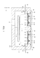
- FIG. 1 is a cross-sectional view of a plasma processing apparatus according to an exemplary embodiment of the present invention.
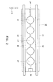
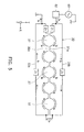
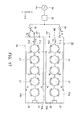
- FIG. 2 is a plan view of the antenna of FIG. 1 .
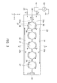
- FIG. 3 is a plan view of the antenna of FIG. 1 , wherein the cooling pipe is omitted.
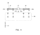
- FIG. 4 is an enlarged cross-sectional view along Line A-A of FIG. 3 .
- FIG. 5 is an equivalent circuit diagram of the antenna of FIG. 3 .
- FIG. 6 is an enlarged plan view of the opening of the antenna of FIG. 3 .
- FIG. 7 is a cross-sectional view of go-and-return conductors disposed in the up-down direction.
- FIG. 8 is a schematic view of the antenna of FIG. 3 with dimensions represented.
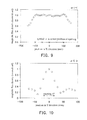
- FIG. 9 is a graph illustrating the measurement results of the magnetic flux density distribution along the X direction of the antenna of FIG. 8 .
- FIG. 10 is a graph illustrating the measurement results of the magnetic flux density distribution along the Y direction of the antenna of FIG. 8 .
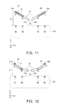
- FIG. 11 is a cross-sectional view of an antenna according to another exemplary embodiment of the present invention, wherein the figure corresponds to the cross-sectional view shown in FIG. 4 .
- FIG. 12 is a cross-sectional view of an antenna according to another exemplary embodiment of the present invention, wherein the figure corresponds to the cross-sectional view shown in FIG. 4 .
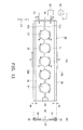
- FIG. 13A is a schematic plan view of an antenna according to another exemplary embodiment of the present invention.
- FIG. 13B is a schematic cross-sectional view of the antenna of FIG. 13A .
- FIG. 14 is a schematic view of the opening of an antenna, wherein the diameter of the opening is changed and the magnetic flux density distributed along the vertical direction of the conductor surface around the opening is measured.
- FIG. 15 is a graph illustrating the measurement results of the magnetic flux density distributed along the vertical direction of the conductor surface around the opening of the antenna of FIG. 14 .
- FIG. 16 is a plan view showing that a plurality of antennas are disposed in parallel and high frequency power is parallelly supplied thereto by a common high frequency power source according to an exemplary embodiment of the present invention.
- FIG. 17 is a plan view showing that a plurality of antennas are disposed in parallel and high frequency power is parallelly supplied thereto by a common high frequency power source according to another exemplary embodiment of the present invention.
- FIG. 1 A plasma processing apparatus according to an exemplary embodiment of the present invention is shown in FIG. 1 , and FIG. 2 to FIG. 4 show the antenna 30 of FIG. 1 . Except FIG. 1 and FIG. 2 , in order to simplify the figures, the cooling pipe is omitted in the figures. The cooling pipe is also omitted in the figures of exemplary embodiments described later.
- the X direction, Y direction and Z direction are orthogonal to each other.
- the Z direction is the direction of the perpendicular line 3 standing on a surface of the substrate 2.
- the Y direction is the direction orthogonal to the perpendicular line 3. These directions are respectively known as the up-down direction Z and the left-right direction Y to simplify the descriptions.
- the X direction is the direction orthogonal to the perpendicular line 3 and is the longitudinal direction of the antenna 30.
- the X direction and Y direction are horizontal, but it is not limited thereto. The foregoing descriptions of the X direction, Y direction and Z direction are applicable in other figures.
- the apparatus is an inductively-coupled plasma (ICP) type plasma processing apparatus.
- ICP inductively-coupled plasma
- a high frequency current I R from a high frequency power source 60 is applied to an antenna 30, that is substantially straight in a plan view of the antenna, in the apparatus so that an electric field is induced in a vacuum container 4 to generate a plasma 50, and the plasma 50 is used to perform a plasma treatment to a substrate 2.
- substantially straight not only represents “a straight status” according to the plan meaning of the words, but also represents “a nearly straight status”.
- a holder 10 is disposed in the vacuum container 4.
- the substrate 2 can be substrates used in flat panel displays (FPD) such as liquid crystal displays and organic electroluminescent displays, flexible substrates used in flexible displays, substrates used in solar cells of semiconductor display or the like; the present invention is not limited thereto.
- FPD flat panel displays
- the planar shape of the substrate 2 can be circular or quadrilateral, but the planar shape is not restricted in the present invention.
- the treatment process to the substrate 2 is forming a film by means of plasma CVD (chemical vapour deposition) process, etching, ashing, sputtering and the like.
- plasma CVD chemical vapour deposition
- the plasma processing apparatus is respectively called, a plasma CVD apparatus if it is used for the plasma CVD process, a plasma etching apparatus for etching process, a plasma ashing apparatus for ashing process, and a plasma sputtering apparatus for sputtering process.
- the plasma processing apparatus has a vacuum container 4 made of metal and the interior of the vacuum container 4 is vacuumed by using a vacuum exhaust device 8.
- a gas 24 is brought into the vacuum container 4 through an inlet pipe 22.
- a plurality of inlet pipes 22 are disposed along the longitudinal direction X of the antenna 30, and a diffusion plate 26 can be disposed in front of the inlet pipes 22 so as to diffuse the gas 24.
- the gas 24 may be any gas which is appropriate to the processing content of the substrate 2.
- the gas 24 is a source gas and a diluted source gas (e.g., H 2 ). More specifically, the source gas 24 is SiH 4 for a Si film, SiH 4 +NH 3 for a SiN film, SiH 4 +O 2 for a SiO 2 film formed on the substrate 2, respectively.
- a planar-shaped opening 7 is disposed at the ceiling 6 of the vacuum container 4, wherein the opening 7 corresponds to the planar shape of the antenna 30.
- the opening 7 corresponds to the planar shape of the antenna 30.
- two openings 7 are disposed and an antenna 30 is disposed in each of the openings 7.
- a cover plate 44 e.g., flange
- a packing 46 used for vacuum sealing is disposed between each of the cover plates 44 and ceilings 6.
- Each of the cover plates 44 can be made of dielectric material, but in the present embodiment, each of the cover plates 44 is made of metal and electrically grounded together with the vacuum container 4. Thus, the high frequency leakage of the antenna 30 to the outside can be prevented.
- each of the antennas 30, two long rectangular conductor plates 31, 32 are disposed on the same plane (namely in the embodiment, the same plane parallel to the XY plane) along the surface of the substrate 2 in the X direction, wherein the two rectangular conductor plates 31, 32 are closely and parallelly disposed to each other with an interval 34 therebetween.
- a side of one of the two rectangular conductor plates 31, 32 is opposite to a side of the other with an interval 34 therebetween and the two rectangular conductor plates 31, 32 are close and parallel to each other.
- an end of a side in the longitudinal direction X of one of the two rectangular conductor plates 31 and an end of a side in the longitudinal direction X of the other rectangular conductor plate 32 are connected through a conductor 33.
- the conductor 33 can be integrally or separately formed with the two rectangular conductor plates 31, 32.
- the material of the conductor 33 and each of the two rectangular conductor plates 31, 32 is, for example, copper (more particularly oxygen-free copper OFC), aluminum and the like, but it is not restricted thereto.
- a high frequency power is supplied to the two rectangular conductor plates 31, 32 which form the antenna 30 by a high frequency power source 60 through a matching circuit 44 so that a high frequency current I R (go-and-return current) flows in opposite directions in the two rectangular conductor plates 31, 32 (since it is a high frequency, the direction of the high frequency current I R reverses according to the time, and it is similar in the following).
- a high frequency current I R go-and-return current
- an end, opposite to theconductor 33, of a side of the rectangular conductor plate 31 is referred as a power feeding point
- an end, opposite to the conductor 33, of a side of the other rectangular conductor plate 32 is referred as an endpoint.
- the endpoint can be directly connected to the ground, and connected to the ground via a condenser, and it is similar in the antennas 30 of other embodiments.
- high frequency power source 60 for the sake of simplifying the descriptions, only one high frequency power source 60, matching circuit 62 and antenna 30 are illustrated in FIG. 3 and FIG 4 , but the high frequency power source 60 and the matching circuit 62 can be commonly used to a plurality of antennas 30. Namely, a common high frequency power source 60 can be parallelly supplied high frequency power to a plurality of antennas 30 which are disposed in parallel to each other. The exemplary embodiments thereof are described later.
- a high frequency magnetic field is generated due to the high frequency current I R , and a high frequency current I R and an electric field to the opposite direction are induced due to the high frequency magnetic field. Due to the electric field, within the vacuum container 4, electrons are accelerated, the gas 24 near the antenna 30 is ionized and plasma 50 is formed near the antenna 30. The plasma 50 is diffused into the surrounding of the substrate 2, and the substrate 2 is treated by using the plasma 50.
- the frequency of the high frequency power output from the high frequency power source 60 is 13.56 MHz in general, but the present invention is not limited thereto.
- the interval 34 is formed between the sides 31a, 32a, located beside the interval 34, of the two rectangular conductor plates 31, 32 (in other words, the sides adjacent to the interval 31a, 32a).
- a plurality of notches 35, 36 are respectively disposed on the sides adjacent to the interval 31a, 32a and the interval 34 is sandwiched between the notches 35, 36.
- a space formed by a notch 35, a notch 36 and the interval 34 sandwiched therebetween is defined as an opening 37.
- the openings 37 are formed along the longitudinal direction X of the antenna 30.
- the quantity of the openings 37 can be five, but it is not limited thereto. It is similar in the antennas 30 of other embodiments.
- Each of the notches 35, 36 can be symmetrically formed by taking the interval 34 as center portion.
- the shape of each of the openings 37 is circular as shown in the figure, but it can also be square, rectangular or the like.
- the two rectangular conductor plates act like the go-and-return conductor structure and the high frequency current I R flows in opposite directions therein, the effective inductance of the antenna 30 is decreased due to the mutual inductance existing between the go-and-return conductors (the two rectangular conductor plates) 31, 32.
- the total impedance Z T of two go-and-return conductors which are closely disposed in parallel, described in books, such as theory of electricity as a differential connection, can be represented by the following equation.
- R represents resistance of each conductor
- L represents self-inductance of each conductor
- M represents mutual inductance of the two conductors.
- the inductance L T in the total impedance Z T is described in the following equation.
- the combination of the self inductance and the mutual inductance is defined as an effective inductance in this specification.
- the potential difference generated between the two ends of the antenna 30 in the longitudinal direction X can be decreased.
- the uniformity of the plasma density distribution along the longitudinal direction X of the antenna 30 can also be improved.
- the potential of the plasma 50 can be decreased, the energy of the charged particles (e.g., ions) impinged to the surface of the substrate 2 from the plasma 50 can be decreased.
- the damage caused to the film can be decreased and the film quality can be enhanced.
- the antenna 30 having a longer length in the longitudinal direction X since the potential of the antenna 30 can be decreased and the plasma potential can be decreased, it is easier to design a larger substrate 2 corresponding to the longer antenna 30.
- the uniformity of the plasma density distribution along the longitudinal direction X of the antenna 30 can be increased, the uniformity of the substrate treatment along the longitudinal direction X of the antenna 30 can also be enhanced. For example, in the case of forming a film on the substrate 2 by the plasma 50, the uniformity of the thickness distribution of the film along the longitudinal direction X of the antenna 30 can be improved.
- the high frequency current I R mainly intends to flow to the ends of each side of the two rectangular conductor plates 31, 32 because of the skin effect.
- the high frequency current I R can flow in opposite directions between the sides which are closely located, compared to the sides opposite to the interval 34 (defined as the sides facing away from the interval) 31b, 32b, both the inductance and the impedance become smaller.
- both the inductance and the impedance of the sides adjacent to the interval 31a, 32a can be smaller. This is in accordance with the principle previously described in Equation 1 and Equation 2. That is, the effective inductance of the sides adjacent to the interval 31a, 32a is decreased due to the mutual inductance.
- the matching circuit of the antenna 30 shown in FIG. 3 is illustrated in FIG. 5 .
- the impedances separately distributed on the sides adjacent to the interval 31 a, 32a and sides facing away from the interval 31b, 32b are respectively represented by Z 1 , Z 3 , Z 2 and Z 4 . Accordingly, the impedances Z 1 , Z 3 of the sides adjacent to the interval 31a, 32a are smaller than the impedances Z 2 , Z 4 of the sides facing away from the interval 31b, 32b.
- the high frequency current I R can flow more along the sides adjacent to the interval 31a, 32a and the openings 37 formed thereon.
- the openings 37 are separately arranged in the longitudinal direction X of the antenna 30 and having the function similar to coil and simple structure, the openings 37 can be formed like a plurality of coils connected in series. Accordingly in such simple structure, a strong magnetic field may be generated around each of the openings 37 and success rate of plasma generating can be increased.
- the forming of magnetic field around each of the openings 37 is described with the reference of FIG. 6 . Since the high frequency current I R flows in opposite directions along the opening 37 (the cutouts) and the magnetic fields 64, 65 respectively generated thereon are in the same direction in the opening 37, the magnetic field intensity becomes the sum of that of the two magnetic fields 64, 65, and thus a strong magnetic field can be generated. In addition, the intensity of the magnetic field 66 which is perpendicular (i.e., direction Z) to the antenna surface (the conductor surface) can be increased.
- the inductive current 68 flowing in the plasma 50 and induced by the magnetic field can make the high frequency current I R flow in the opposite directions by orbiting the magnetic field 66.
- the inductance of the antenna 30 can be decreased and the potential difference generated between the two ends of the antenna 30 in the longitudinal direction X can also be decreased. The effect is as described above.
- two plate-shaped conductors (go-and-return conductors) 71, 72 can be closely disposed in the up-down direction with respect to the generating region of plasma 50.
- the magnetic fields 73, 74, formed by the high frequency current I R which flows in opposite directions in the two conductors 71, 72, flow in opposite directions in the generating region of plasma 50 the magnetic field intensity becomes the difference between the intensities of the two magnetic fields 73, 74 and thus is decreased. Therefore, both the plasma generating efficiency and the high frequency power utilization efficiency can be increased.
- a straight cooling pipe 42 can be mounted on each of the two rectangular conductor plates 31, 32.
- the cooling structure is simple and easy for manufacturing. It is the same in the case of antenna 30 described in the following.
- FIG. 8 is a schematic view of the antenna of FIG. 3 with dimensions represented.
- the center of each of the openings 37 located at the midpoint of the longitudinal direction X is defined as the origin O of the X, Y directions.
- the measurement results of the magnetic flux density distribution along the X direction of the antenna of FIG. 8 are illustrated in FIG. 9
- the measurement results of the magnetic flux density distribution along the Y direction of the antenna of FIG. 8 are illustrated in FIG. 10 .
- the measurement conditions are as follows. Namely, the length L 1 of the two rectangular conductor plates 31, 32 is 30 mm, the width W 1 is 50 mm, the width W 2 of the interval 34 is 5 mm, the quantity of the openings 37 is 5, the diameter D of each of the openings 37 is 40 mm, the distance between every two adjacent openings 37 is 50 mm.
- the material of the two rectangular conductor plates 31, 32 is copper, the frequency of the high frequency power is 13.56 MHz, the output of the high frequency power source 60 is 3 W.
- the reflected power is 0 W.
- the magnetic flux density is measured in the range from the conductor surface to the position of 30 mm.
- the plasma 50 is not generated.
- pulsation at the openings 37 is less and a uniform and good magnetic flux density distribution is obtained along the longitudinal direction X of the antenna 30.
- the reasons can be (a) in the position from the conductor surface to 30 mm distance, the magnetic flux density generated around the openings 37 keeps spreading in the X direction, (b) since the width W 2 of the interval 34 is 5 mm, the magnetic field occurs even at the connecting portion 38 between the openings 37.
- the magnetic field occurring around the center of the openings 37 is strong, whereas the magnetic field occurring around the outer edges 31b, 32b ( ⁇ 50 mm) of the two rectangular conductor plates 31, 32 is weak. As previously described, it represents that the high frequency current flowing through the outer edges 31b, 32b is small.
- the sizes of the openings 37 and the distances between the openings 37 can also be designed to be different along the longitudinal direction X of the antenna 30. Or, both of designing to be the same and designing to be different may be used. If necessary, the openings 37 located around the center portion of the longitudinal direction X can also be omitted. Accordingly, the plasma density distribution in the longitudinal direction X of the antenna 30 can be adjusted. It is the same in the case of antenna 30 described in the following.
- the size (the diameter) of the opening 37 is changed and the magnetic flux density distributed along the vertical direction (Z direction) of the conductor surface around the opening 37 is measured and the measurement results are shown in FIG. 15 .
- the measurement conditions are as follows. The dimensions of the two rectangular conductor plates 31, 32 and the interval 34 are as described in FIG. 14 , the material of the two rectangular conductor plates 31, 32 is copper, the frequency of the high frequency power is 13.56 MHz and the high frequency power output during the measurement is 3 W. The magnetic flux density in the range from the conductor surface to 30 mm distance is measured. The plasma is not generated.
- the magnetic flux density around the opening 37 is increased since the dimension of the opening 37 is increased.
- the plasma density distribution in the longitudinal direction X of the antenna 30 has the tendency to be smaller at the two terminals than other places. If simply described the reason, the plasma can be diffused from two sides at the central portion whereas the plasma just can be diffused from single side at each of the two terminals.
- the openings 37 located at the two ends of the antenna 30 in the longitudinal direction X can be designed to be larger than the rest of the openings 37 located at other places. Accordingly, according to the measurement results illustrated in FIG. 15 , since the magnetic flux density around the openings 37 located at the two ends is increased and the plasma density is increased, the uniformity of the plasma density distribution along the longitudinal direction X of the antenna 30 can be improved. As a result, the uniformity of the substrate treatment along the longitudinal direction X of the antenna 30 can also be enhanced. For example, in the case of forming a film on the substrate 2 by the plasma 50, the uniformity of the film thickness distribution along the longitudinal direction X of the antenna 30 can be increased.
- the distance between the openings 37 located at the two ends of the antenna 30 in the longitudinal direction X (the distance between the adjacent openings 37) can be designed to be smaller than the distances between other openings 37. Accordingly, since the magnetic flux density around the openings 37 located at the two ends can be increased and the plasma density can be increased, the uniformity of the plasma density distribution along the longitudinal direction X of the antenna 30 can be improved. As a result, the uniformity of the substrate treatment along the longitudinal direction X of the antenna 30 can also be enhanced. For example, in the case of forming a film on the substrate 2 by the plasma 50, the uniformity of the film thickness distribution along the longitudinal direction X of the antenna 30 can be increased.
- the openings 37 around the center portion in the longitudinal direction X can be omitted.
- the openings 37 located at the two ends of the antenna 30 in the longitudinal direction X can be designed to be larger than the rest of the openings 37 located at other places, and the distance between the openings 37 located at the two ends of the antenna 30 in the longitudinal direction X can also be designed to be smaller than the distances between other openings 37.
- the dielectric plate 52 is disposed so as to obstruct the antenna 30 from the plasma 50.
- the dielectric plate 52 can be closely disposed to the antenna 30. In this way, the advantage of widening the generating space of the plasma 50 can be achieved.
- the dielectric plates 52 are respectively disposed around the inlet of each of the openings 37 disposed in the antenna 30.
- the dielectric plates 52 can be directly disposed around the inlet of the openings 37, and the dielectric plates 52 can also be disposed by using the supporting plates 54 as shown in the embodiment.
- a common dielectric plate 52 can also be disposed for a plurality of antennas 30. It is the same in the case of antenna 30 described in the following.
- the dielectric plate 52 can consist of, for example, silicon plates or ceramics such as quartz, aluminum, silicon carbide or the like.
- the surface of the antenna 30 can be prevented from being sputtered by the charged particles (mainly ions) in the plasma 50.
- the charged particles mainly ions
- electrons which form the plasma 50 are lighter and the mobility thereof is much larger than the ions, the escaping of the electrons impinged to the antenna 30 can be avoided due to the dielectric plate 52. Therefore, the increase of the plasma potential can be suppressed.
- the antenna 30 located in the vacuum container 4 can be buried in the dielectric material 48.
- the antenna 30 can also be buried in the dielectric material 48. More specifically, the whole antenna 30 disposed in the opening 7 including the space from the bottom of the antenna 30 to the cover plate 44 is buried in the dielectric material 48. It is the same in the case of antenna 30 described in the following.
- the dielectric material 48 consists of insulating inorganic materials such as ceramics and insulating resins.
- the gas 24 may be diffused to a portion of the antenna 30 located in the vacuum container 4 if the dielectric material 48 is not disposed. Since the diffused gas 24 may be ionized and may generate or may not generate plasma nearby the antenna 30, the instability of the plasma required for substrate treatment is increased.
- the gas 24 diffusing to vicinity of the antenna 30 can be prevented by burying the antenna 30 in the dielectric material 48, the unnecessary plasma close to the antenna 30 located in the vacuum container 4 is prevented to be generated. Accordingly, inconvenience due to the increase of instability of the plasma 50 required for substrate treatment and decreasing of utilization efficiency of the high frequency power can be prevented.
- the two rectangular conductor plates 31, 32 of the antenna 30 are configured in a V-shape cross-sectional structure, wherein the V-shape cross-sectional structure is separated relatively wide at a side facing away from the surface of the substrate 2 (in other words, the opposite side of generating region of the plasma 50) and the two sides 31a, 32a of the two rectangular plates 31, 32 adjacent to the interval 34 can be closely disposed in parallel to each other with the interval 34 therebetween.
- the disposing of the cooling pipes 42, the dielectric material 48 and the dielectric plate 52 are the same to the embodiment shown in FIG. 1 .
- the plasma 50 is generated by the high frequency current I R , and the high frequency current I R and the induced current which flow in an opposite direction flow through the two rectangular conductor plates 31, 32 in the plasma 50, thus both the inductance and the impedance of the antenna 30 can be decreased, according to the principle which is previously described in accordance with Equation 1 and Equation 2.
- the two rectangular conductor plates 31, 32 configured in a V-shape cross-sectional structure
- the two sides 31a, 32a of the two rectangular plates 31, 32 adjacent to the interval 34 can be closely disposed in parallel to each other with the interval 34 therebetween, and the distance L 2 between the sides 31b, 32b facing away from the interval 34 and the surface of the substrate 2 is larger than the distance between the sides 31a, 32a adjacent to the interval 34 and the surface of the substrate 2, the decrease of the inductance is fewer and the impedance is increased.
- the degree of inclination of the two rectangular conductor plates 31, 32 can be appropriately prescribed, wherein the larger the degree of inclination is, the effect of the difference of inductance and impendence between the sides 31a, 32a adjacent to the interval 34 and the sides 31b, 32b facing away from the interval 34 may become larger.
- the two rectangular conductor plates 31, 32 are configured in a manner that the two rectangular conductor plates 31, 32 are bent in a short side direction to form a U-shape cross-sectional structure, wherein the U-shape cross-sectional structure is separated relatively wide at a side facing away from the surface of the substrate 2 (in other words, the opposite side of generating region of the plasma 50) and the two sides 31 a, 32a of the two rectangular plates 31, 32 adjacent to the interval 34 are closely disposed in parallel to each other with the interval 34 therebetween. It may be planar near the openings 37.
- the disposing of the cooling pipes 42, the dielectric material 48 and the dielectric plate 52 are the same to the embodiment shown in FIG. 1 .
- the two rectangular conductor plates 31, 32 are configured in a manner that the two rectangular conductor plates 31, 32 are bent in a short side direction to form a U-shape cross-sectional structure and disposed on the surface of the substrate 2 and the distance L 2 between the sides 31b, 32b facing away from the interval 34 and the surface of the substrate 2 is larger than the distance between the sides 31a, 32a adjacent to the interval 34 and the surface of the substrate 2, the decrease of the inductance is fewer and the impedance is increased.
- the degree of bending of the two rectangular conductor plates 31, 32 can be appropriately prescribed, wherein the larger the degree of bending is, the effect of the difference of inductance and impendence between the sides 31a, 32a adjacent to the interval 34 and the sides 31b, 32b facing away from the interval 34 may become larger.
- peripheries of the sides 31b, 32b facing away from the interval 34 of the two rectangular conductor plates 31, 32 of the antenna 30 is covered by a conductor 76, wherein the specific resistance of the conductor 76 is greater than the specific resistance of the material of the two rectangular conductor plates 31, 32, and the thickness of the conductor 76 is equal to or greater than a skin depth of the high frequency current I R flowing through the conductor 76.
- the high frequency current I R can mainly flow through the ends of each side of the two rectangular conductor plates 31, 32. Therefore, referring to the sides 31b, 32b facing away from the interval 34 of the two rectangular conductor plates 31, 32, the peripheries (the top, bottom and end) of the sides 31b, 32b facing away from the interval 34 are covered by the conductor 76.
- the width W 4 of the conductor 76 in the Y direction is about 10 mm to 20 mm, for example, and it is sufficient.
- the conductor 76 for covering as mentioned above can be simply formed by performing with a plating method onto the sides 31b, 32b facing away from the interval 34 of the two rectangular conductor plates 31, 32.
- the material of the conductor 76 can be copper, aluminum or the like as above mentioned. Instead, the material of the conductor 76 with a large specific resistance can be, for example, nickel, iron or the like. Those materials not only have large specific resistance but also have large magnetic permeability.
- the frequency f is 13.56 MHz.
- the magnetic permeability ⁇ is about 2.4 ⁇ 10 -4 N/A2
- the specific resistance ⁇ is about 6.84 ⁇ 10 -8 ⁇ m
- the conductivity ⁇ is about 14.5 ⁇ 10 6 ⁇ m
- the skin depth ⁇ is about 1.47 ⁇ m. Accordingly, the thickness of the conductor 76 can be more than above value.
- the conductor 76 Since the conductor 76 is covered and due to the skin effect the high frequency current I R flowing through the sides 31b, 32b facing away from the interval 34 of the rectangular conductor plates 31, 32 mainly flows through the conductor 76 having a larger specific resistance, the impedance of the sides 31b, 32b facing away from the interval 34 of the two rectangular conductor plates 31, 32 is increased. As a result, since more high frequency current I R can flow along the sides 31a, 32a adjacent to the interval 34 and the openings 37 formed on the sides 31a, 32a adjacent to the interval 34 of the two rectangular conductor plates 31, 32, the high frequency power can be effectively supplied for plasma generating. Accordingly, both the plasma generating efficiency and the high frequency power utilization efficiency can be increased.
- a plurality of the antennas 30 described above are parallelly disposed in the Y direction.
- High frequency power from a common high frequency power source 60 can be supplied in parallel to the antennas 30.
- the structure of each of the antennas 30 is the same as aforementioned.
- the high frequency power source 60 (more specifically the matching circuit 62 connected thereto) and each of the antennas 30 can be connected via the variable impedance 78 as shown in the figures, and they can also be directly connected to each other.
- the variable impedance 78 can be the variable inductance shown in the figure, can also be a variable condenser (a variable capacitance), or a combination thereof. Since the impedance of the feeding circuit can be increased by inserting the variable inductance, it is possible to suppress the current of the antenna 30 where the high frequency current I R is excessively flowed. Since if the inductive reactance is greater the capacitive reactance is increased and the impedance of the feeding circuit can be decreased by inserting the variable condenser, it is possible to increase the current of the antenna 30 where the high frequency current I R is hard to flow.
- high frequency power from a common high frequency power source 60 is supplied in parallel to each of the antennas 30 in a manner that the high frequency current I R flowing through the adjacent antennas 30 at the adjacent rectangular conductor plates 31, 32 at the two sides 32b, 31b facing away from the interval 34 can be in opposite directions
- high frequency power from a common high frequency power source 60 is supplied in parallel to each of the antennas 30 in a manner that the high frequency current I R flowing through the adjacent antennas 30 at the adjacent rectangular conductor plates 31, 32 at the two sides 32b, 31b facing away from the interval 34can be in the same direction.
- the quantity of the antennas 30 is not limited to be two as shown in the examples, and the antennas 30 can be more than two.
- the example shown in FIG. 17 is preferable. This is due to the following reasons.
Landscapes
- Chemical & Material Sciences (AREA)
- Engineering & Computer Science (AREA)
- Physics & Mathematics (AREA)
- Plasma & Fusion (AREA)
- Organic Chemistry (AREA)
- General Chemical & Material Sciences (AREA)
- Chemical Kinetics & Catalysis (AREA)
- Materials Engineering (AREA)
- Mechanical Engineering (AREA)
- Metallurgy (AREA)
- Analytical Chemistry (AREA)
- Electromagnetism (AREA)
- Spectroscopy & Molecular Physics (AREA)
- Plasma Technology (AREA)
- Chemical Vapour Deposition (AREA)
- Drying Of Semiconductors (AREA)
Applications Claiming Priority (1)
| Application Number | Priority Date | Filing Date | Title |
|---|---|---|---|
| JP2011245408A JP5018994B1 (ja) | 2011-11-09 | 2011-11-09 | プラズマ処理装置 |
Publications (2)
| Publication Number | Publication Date |
|---|---|
| EP2592644A2 true EP2592644A2 (fr) | 2013-05-15 |
| EP2592644A3 EP2592644A3 (fr) | 2016-01-06 |
Family
ID=46888899
Family Applications (1)
| Application Number | Title | Priority Date | Filing Date |
|---|---|---|---|
| EP12181447.9A Withdrawn EP2592644A3 (fr) | 2011-11-09 | 2012-08-23 | Appareil de traitement à plasma |
Country Status (6)
| Country | Link |
|---|---|
| US (1) | US8394232B1 (fr) |
| EP (1) | EP2592644A3 (fr) |
| JP (1) | JP5018994B1 (fr) |
| KR (1) | KR101257005B1 (fr) |
| CN (1) | CN102833937B (fr) |
| TW (1) | TWI402002B (fr) |
Families Citing this family (4)
| Publication number | Priority date | Publication date | Assignee | Title |
|---|---|---|---|---|
| JP2013134835A (ja) * | 2011-12-26 | 2013-07-08 | Nissin Electric Co Ltd | プラズマ処理装置 |
| KR101582838B1 (ko) * | 2013-08-23 | 2016-01-12 | 니신 일렉트릭 컴패니 리미티드 | 플라즈마 처리장치 |
| KR102340365B1 (ko) * | 2018-02-28 | 2021-12-16 | 주식회사 인포비온 | 유도 결합형 플라즈마 소스용 안테나 구조 |
| JP6708887B2 (ja) * | 2018-09-25 | 2020-06-10 | 株式会社プラズマイオンアシスト | プラズマ処理装置、アンテナ導体又は/及び導電性部材の製造方法 |
Citations (1)
| Publication number | Priority date | Publication date | Assignee | Title |
|---|---|---|---|---|
| WO2009142016A1 (fr) | 2008-05-22 | 2009-11-26 | 株式会社イー・エム・ディー | Appareil de génération de plasma et appareil de traitement par plasma |
Family Cites Families (12)
| Publication number | Priority date | Publication date | Assignee | Title |
|---|---|---|---|---|
| JP3598717B2 (ja) * | 1997-03-19 | 2004-12-08 | 株式会社日立製作所 | プラズマ処理装置 |
| JPH11317299A (ja) * | 1998-02-17 | 1999-11-16 | Toshiba Corp | 高周波放電方法及びその装置並びに高周波処理装置 |
| JP2000299199A (ja) * | 1999-04-13 | 2000-10-24 | Plasma System Corp | プラズマ発生装置およびプラズマ処理装置 |
| US6744213B2 (en) * | 1999-11-15 | 2004-06-01 | Lam Research Corporation | Antenna for producing uniform process rates |
| KR100797423B1 (ko) * | 2000-05-17 | 2008-01-23 | 가부시키가이샤 아이에이치아이 | 플라즈마 cvd 장치 및 방법 |
| JP4770029B2 (ja) * | 2001-01-22 | 2011-09-07 | 株式会社Ihi | プラズマcvd装置及び太陽電池の製造方法 |
| JP2005079416A (ja) * | 2003-09-02 | 2005-03-24 | Hitachi Ltd | プラズマ処理装置 |
| JP2005285564A (ja) * | 2004-03-30 | 2005-10-13 | Mitsui Eng & Shipbuild Co Ltd | プラズマ処理装置 |
| JP4592576B2 (ja) * | 2005-12-09 | 2010-12-01 | 三菱重工業株式会社 | 放電電極、薄膜製造装置及び太陽電池の製造方法 |
| US20100279438A1 (en) * | 2009-05-01 | 2010-11-04 | Taiwan Semiconductor Manufacturing Company, Ltd. | Apparatus and method of in-situ identification for contamination control in semiconductor fabrication |
| WO2011058608A1 (fr) * | 2009-11-13 | 2011-05-19 | 日新電機株式会社 | Appareil de traitement au plasma |
| WO2011108219A1 (fr) * | 2010-03-03 | 2011-09-09 | 三井造船株式会社 | Appareil de formation de film mince |
-
2011
- 2011-11-09 JP JP2011245408A patent/JP5018994B1/ja not_active Expired - Fee Related
-
2012
- 2012-07-10 KR KR1020120074957A patent/KR101257005B1/ko not_active Expired - Fee Related
- 2012-08-23 US US13/592,346 patent/US8394232B1/en not_active Expired - Fee Related
- 2012-08-23 EP EP12181447.9A patent/EP2592644A3/fr not_active Withdrawn
- 2012-08-24 CN CN201210306854.3A patent/CN102833937B/zh not_active Expired - Fee Related
- 2012-09-06 TW TW101132524A patent/TWI402002B/zh not_active IP Right Cessation
Patent Citations (1)
| Publication number | Priority date | Publication date | Assignee | Title |
|---|---|---|---|---|
| WO2009142016A1 (fr) | 2008-05-22 | 2009-11-26 | 株式会社イー・エム・ディー | Appareil de génération de plasma et appareil de traitement par plasma |
Also Published As
| Publication number | Publication date |
|---|---|
| CN102833937B (zh) | 2015-05-27 |
| KR101257005B1 (ko) | 2013-04-26 |
| CN102833937A (zh) | 2012-12-19 |
| JP2013101862A (ja) | 2013-05-23 |
| JP5018994B1 (ja) | 2012-09-05 |
| TWI402002B (zh) | 2013-07-11 |
| EP2592644A3 (fr) | 2016-01-06 |
| TW201306672A (zh) | 2013-02-01 |
| US8394232B1 (en) | 2013-03-12 |
Similar Documents
| Publication | Publication Date | Title |
|---|---|---|
| KR101591404B1 (ko) | 플라즈마 생성장치 및 플라즈마 처리장치 | |
| CN105706213B (zh) | 等离子体产生设备 | |
| US8372239B2 (en) | Plasma processing apparatus | |
| US20060254519A1 (en) | Locally-efficient inductive plasma coupling for plasma processing system | |
| CN104427736B (zh) | 等离子体处理装置 | |
| EP1976346A1 (fr) | Appareil de génération de plasma | |
| US8394232B1 (en) | Plasma processing apparatus | |
| JP5419055B1 (ja) | プラズマ処理装置およびプラズマ処理方法 | |
| CN104081492B (zh) | 电浆产生装置 | |
| KR101572100B1 (ko) | 복합 주파수를 이용한 대면적 플라즈마 반응기 | |
| TWI298005B (en) | Plasma apparatus | |
| KR101384583B1 (ko) | 다중 무선 주파수 안테나를 갖는 유도 결합 플라즈마반응기 | |
| KR101196422B1 (ko) | 플라즈마 처리장치 | |
| KR20110006070U (ko) | 자화된 유도결합형 플라즈마 처리장치 | |
| KR20100129369A (ko) | 수직 듀얼 챔버로 구성된 대면적 플라즈마 반응기 | |
| KR101214361B1 (ko) | 플라즈마 발생장치 | |
| JP5273759B1 (ja) | プラズマ処理装置およびプラズマ処理方法 | |
| JP5447725B1 (ja) | プラズマ処理装置 | |
| JP2013175480A (ja) | プラズマ処理装置およびプラズマ処理方法 | |
| JP2013131295A (ja) | プラズマ処理装置 | |
| WO2012176242A1 (fr) | Dispositif de traitement par plasma | |
| KR20080069755A (ko) | 유도 결합 플라즈마 반응기 | |
| JP2012226888A (ja) | プラズマ処理装置 | |
| JP2012033323A (ja) | プラズマ発生用電極及びプラズマ発生装置 | |
| KR20110055306A (ko) | 급전손실 저감을 위한 용량 결합 플라즈마 반응기 |
Legal Events
| Date | Code | Title | Description |
|---|---|---|---|
| PUAI | Public reference made under article 153(3) epc to a published international application that has entered the european phase |
Free format text: ORIGINAL CODE: 0009012 |
|
| AK | Designated contracting states |
Kind code of ref document: A2 Designated state(s): AL AT BE BG CH CY CZ DE DK EE ES FI FR GB GR HR HU IE IS IT LI LT LU LV MC MK MT NL NO PL PT RO RS SE SI SK SM TR |
|
| AX | Request for extension of the european patent |
Extension state: BA ME |
|
| PUAL | Search report despatched |
Free format text: ORIGINAL CODE: 0009013 |
|
| AK | Designated contracting states |
Kind code of ref document: A3 Designated state(s): AL AT BE BG CH CY CZ DE DK EE ES FI FR GB GR HR HU IE IS IT LI LT LU LV MC MK MT NL NO PL PT RO RS SE SI SK SM TR |
|
| AX | Request for extension of the european patent |
Extension state: BA ME |
|
| RIC1 | Information provided on ipc code assigned before grant |
Ipc: C23C 16/505 20060101ALI20151201BHEP Ipc: H01J 37/32 20060101AFI20151201BHEP |
|
| STAA | Information on the status of an ep patent application or granted ep patent |
Free format text: STATUS: THE APPLICATION IS DEEMED TO BE WITHDRAWN |
|
| 18D | Application deemed to be withdrawn |
Effective date: 20160707 |