EP2592736B1 - System und Verfahren zum Überwachen von Schaltharmonischen in einem Gleichstromzwischenkreis - Google Patents
System und Verfahren zum Überwachen von Schaltharmonischen in einem Gleichstromzwischenkreis Download PDFInfo
- Publication number
- EP2592736B1 EP2592736B1 EP12192650.5A EP12192650A EP2592736B1 EP 2592736 B1 EP2592736 B1 EP 2592736B1 EP 12192650 A EP12192650 A EP 12192650A EP 2592736 B1 EP2592736 B1 EP 2592736B1
- Authority
- EP
- European Patent Office
- Prior art keywords
- bus
- current
- module
- sampling rate
- voltage
- Prior art date
- Legal status (The legal status is an assumption and is not a legal conclusion. Google has not performed a legal analysis and makes no representation as to the accuracy of the status listed.)
- Active
Links
- 238000000034 method Methods 0.000 title claims description 31
- 238000005070 sampling Methods 0.000 claims description 46
- 238000004364 calculation method Methods 0.000 claims description 24
- 238000004891 communication Methods 0.000 claims description 13
- 239000004020 conductor Substances 0.000 claims description 13
- 238000001514 detection method Methods 0.000 claims description 12
- 238000012544 monitoring process Methods 0.000 claims description 8
- 230000008569 process Effects 0.000 claims description 6
- 238000001914 filtration Methods 0.000 claims 1
- 238000007726 management method Methods 0.000 description 40
- 239000003990 capacitor Substances 0.000 description 14
- 230000006870 function Effects 0.000 description 10
- 238000010586 diagram Methods 0.000 description 5
- 230000015654 memory Effects 0.000 description 4
- 230000004044 response Effects 0.000 description 4
- 238000009826 distribution Methods 0.000 description 3
- 238000012986 modification Methods 0.000 description 3
- 230000004048 modification Effects 0.000 description 3
- 238000012546 transfer Methods 0.000 description 3
- 238000006243 chemical reaction Methods 0.000 description 2
- 238000004519 manufacturing process Methods 0.000 description 2
- 238000012545 processing Methods 0.000 description 2
- 230000009467 reduction Effects 0.000 description 2
- 239000007787 solid Substances 0.000 description 2
- 238000003860 storage Methods 0.000 description 2
- 230000000007 visual effect Effects 0.000 description 2
- XUIMIQQOPSSXEZ-UHFFFAOYSA-N Silicon Chemical compound [Si] XUIMIQQOPSSXEZ-UHFFFAOYSA-N 0.000 description 1
- 230000003321 amplification Effects 0.000 description 1
- 230000002238 attenuated effect Effects 0.000 description 1
- 230000005540 biological transmission Effects 0.000 description 1
- 230000001143 conditioned effect Effects 0.000 description 1
- 238000010276 construction Methods 0.000 description 1
- 238000013016 damping Methods 0.000 description 1
- 230000007423 decrease Effects 0.000 description 1
- 230000001419 dependent effect Effects 0.000 description 1
- 238000011161 development Methods 0.000 description 1
- 230000018109 developmental process Effects 0.000 description 1
- 238000002955 isolation Methods 0.000 description 1
- 238000003199 nucleic acid amplification method Methods 0.000 description 1
- 229910052710 silicon Inorganic materials 0.000 description 1
- 239000010703 silicon Substances 0.000 description 1
Images


Classifications
-
- H—ELECTRICITY
- H02—GENERATION; CONVERSION OR DISTRIBUTION OF ELECTRIC POWER
- H02P—CONTROL OR REGULATION OF ELECTRIC MOTORS, ELECTRIC GENERATORS OR DYNAMO-ELECTRIC CONVERTERS; CONTROLLING TRANSFORMERS, REACTORS OR CHOKE COILS
- H02P5/00—Arrangements specially adapted for regulating or controlling the speed or torque of two or more electric motors
- H02P5/74—Arrangements specially adapted for regulating or controlling the speed or torque of two or more electric motors controlling two or more AC dynamo-electric motors
-
- H—ELECTRICITY
- H02—GENERATION; CONVERSION OR DISTRIBUTION OF ELECTRIC POWER
- H02M—APPARATUS FOR CONVERSION BETWEEN AC AND AC, BETWEEN AC AND DC, OR BETWEEN DC AND DC, AND FOR USE WITH MAINS OR SIMILAR POWER SUPPLY SYSTEMS; CONVERSION OF DC OR AC INPUT POWER INTO SURGE OUTPUT POWER; CONTROL OR REGULATION THEREOF
- H02M1/00—Details of apparatus for conversion
- H02M1/14—Arrangements for reducing ripples from DC input or output
- H02M1/15—Arrangements for reducing ripples from DC input or output using active elements
-
- G—PHYSICS
- G01—MEASURING; TESTING
- G01R—MEASURING ELECTRIC VARIABLES; MEASURING MAGNETIC VARIABLES
- G01R19/00—Arrangements for measuring currents or voltages or for indicating presence or sign thereof
- G01R19/25—Arrangements for measuring currents or voltages or for indicating presence or sign thereof using digital measurement techniques
- G01R19/2506—Arrangements for conditioning or analysing measured signals, e.g. for indicating peak values ; Details concerning sampling, digitizing or waveform capturing
- G01R19/2509—Details concerning sampling, digitizing or waveform capturing
-
- G—PHYSICS
- G01—MEASURING; TESTING
- G01R—MEASURING ELECTRIC VARIABLES; MEASURING MAGNETIC VARIABLES
- G01R23/00—Arrangements for measuring frequencies; Arrangements for analysing frequency spectra
- G01R23/16—Spectrum analysis; Fourier analysis
- G01R23/20—Measurement of non-linear distortion
-
- H—ELECTRICITY
- H02—GENERATION; CONVERSION OR DISTRIBUTION OF ELECTRIC POWER
- H02M—APPARATUS FOR CONVERSION BETWEEN AC AND AC, BETWEEN AC AND DC, OR BETWEEN DC AND DC, AND FOR USE WITH MAINS OR SIMILAR POWER SUPPLY SYSTEMS; CONVERSION OF DC OR AC INPUT POWER INTO SURGE OUTPUT POWER; CONTROL OR REGULATION THEREOF
- H02M5/00—Conversion of AC power input into AC power output, e.g. for change of voltage, for change of frequency, for change of number of phases
- H02M5/40—Conversion of AC power input into AC power output, e.g. for change of voltage, for change of frequency, for change of number of phases with intermediate conversion into DC
- H02M5/42—Conversion of AC power input into AC power output, e.g. for change of voltage, for change of frequency, for change of number of phases with intermediate conversion into DC by static converters
- H02M5/44—Conversion of AC power input into AC power output, e.g. for change of voltage, for change of frequency, for change of number of phases with intermediate conversion into DC by static converters using discharge tubes or semiconductor devices to convert the intermediate DC into AC
- H02M5/453—Conversion of AC power input into AC power output, e.g. for change of voltage, for change of frequency, for change of number of phases with intermediate conversion into DC by static converters using discharge tubes or semiconductor devices to convert the intermediate DC into AC using devices of a triode or transistor type requiring continuous application of a control signal
- H02M5/458—Conversion of AC power input into AC power output, e.g. for change of voltage, for change of frequency, for change of number of phases with intermediate conversion into DC by static converters using discharge tubes or semiconductor devices to convert the intermediate DC into AC using devices of a triode or transistor type requiring continuous application of a control signal using semiconductor devices only
- H02M5/4585—Conversion of AC power input into AC power output, e.g. for change of voltage, for change of frequency, for change of number of phases with intermediate conversion into DC by static converters using discharge tubes or semiconductor devices to convert the intermediate DC into AC using devices of a triode or transistor type requiring continuous application of a control signal using semiconductor devices only having a rectifier with controlled elements
-
- G—PHYSICS
- G01—MEASURING; TESTING
- G01R—MEASURING ELECTRIC VARIABLES; MEASURING MAGNETIC VARIABLES
- G01R19/00—Arrangements for measuring currents or voltages or for indicating presence or sign thereof
- G01R19/25—Arrangements for measuring currents or voltages or for indicating presence or sign thereof using digital measurement techniques
- G01R19/2513—Arrangements for monitoring electric power systems, e.g. power lines or loads; Logging
-
- G—PHYSICS
- G01—MEASURING; TESTING
- G01R—MEASURING ELECTRIC VARIABLES; MEASURING MAGNETIC VARIABLES
- G01R31/00—Arrangements for testing electric properties; Arrangements for locating electric faults; Arrangements for electrical testing characterised by what is being tested not provided for elsewhere
- G01R31/40—Testing power supplies
- G01R31/42—AC power supplies
-
- H—ELECTRICITY
- H02—GENERATION; CONVERSION OR DISTRIBUTION OF ELECTRIC POWER
- H02M—APPARATUS FOR CONVERSION BETWEEN AC AND AC, BETWEEN AC AND DC, OR BETWEEN DC AND DC, AND FOR USE WITH MAINS OR SIMILAR POWER SUPPLY SYSTEMS; CONVERSION OF DC OR AC INPUT POWER INTO SURGE OUTPUT POWER; CONTROL OR REGULATION THEREOF
- H02M1/00—Details of apparatus for conversion
- H02M1/0067—Converter structures employing plural converter units, other than for parallel operation of the units on a single load
- H02M1/008—Plural converter units for generating at two or more independent and non-parallel outputs, e.g. systems with plural point of load switching regulators
Definitions
- the subject matter disclosed herein relates generally to a distributed motor drive system and, more specifically, to a system and method for managing harmonic currents present on a direct current (DC) link in a distributed motor drive system.
- DC direct current
- Alternating current (AC) motors receive an AC voltage at the stator of the motor.
- the speed and torque of the motor are controlled by varying the amplitude and frequency of this AC voltage applied to the stator.
- a motor controller rapidly switches solid state devices on and off at a predetermined switching frequency and, thereby, alternately connects or disconnects the terminals of the motor to a DC voltage.
- the motor controller utilizes modulation techniques such as pulse width modulation (PWM) to control the switching and to synthesize waveforms having desired amplitudes and frequencies.
- PWM pulse width modulation
- servo motors such as a process line with multiple stations, a machining center, or an industrial robotic arm
- Each axis requires a motor and a controller to regulate, for example, the speed, position, or torque of the motor.
- the motors are necessarily positioned along the process line or about the machine as needed to actuate a specific motion.
- the motor controllers are typically located within one or more enclosures at a common location.
- developments in the power electronic devices used to control the motor have reduced the size of the components. This reduction in size of the power electronic devices along with a desire to reduce the size of the control enclosures have led to placing at least a portion of the motor controller electronics on the motor itself.
- the inverter section receives a DC voltage via a DC link cable from a DC bus output of the rectifier section in the control enclosure.
- a small amount of capacitance may be connected across the DC link at the inverter section, modulation of the solid state devices in the inverter produces harmonic currents at multiples of the inverter switching frequency, which are, subsequently, conducted on the DC link between the inverter section and the control enclosure.
- the DC link cable extending between the control enclosure and the inverter section can establish a resonant frequency as a function of the length of the DC link cable. If the length of the DC link cable is selected such that the resonant frequency is close to the switching frequency of the inverter, the harmonic current on the DC link may be amplified. To avoid amplification of the harmonic current specific lengths of the DC link cable may be required. Alternately, to compensate for the harmonic content the size of the conductor is increased or the current rating of the conductor is reduced. Each of these options introduces an undesirable cost or limitation in the system.
- EP1482634 A2 describes a motor drive system comprises first and second motor drive amplifiers (3a, 3b), connected to a motor drive power supply (6), which include first and second memories (32a, 32b) which store specifications of the amplifiers (3a, 3b) respectively.
- a memory (52) provided in a power supply unit control circuit (5) stores an overcurrent detection value for detecting an overcurrent according to the specifications of the respective motor drive amplifiers (3a, 3b).
- a microcontroller (51) reads the specifications from the first and second memories (32a, 32b), and integrates overcurrent detection values corresponding to the respective specifications. If a current sensor (7) detects a current exceeding a reference value calculated based on a set integrated value, an overcurrent detection circuit (54) outputs an overcurrent detection signal.
- the system has an overcurrent detection circuit (54) detecting a current flowing in a motor drive power supply. An overcurrent detection value to be detected as an overcurrent by the overcurrent detection circuit is changed. The overcurrent detection circuit outputs an overcurrent detection signal, if a current sensor (7) detects a current exceeding a reference value, which is calculated based on a set integrated value.
- US6198613 B1 describes a method and apparatus for distributing alternating electrical current to motors via a direct current bus is provided.
- the method and apparatus is directed towards a system wherein a plurality of motors may be controlled by individual motor drives.
- AC power is supplied to a single active rectifier circuit (as opposed to one per motor) which maintains unity power factor in the AC power and which develops DC power for a DC distribution system.
- the DC distribution system which comprises a set of controllable contactors, is in turn coupled to a plurality of motor drive units which convert the DC power into properly conditioned AC power for operating associated motors.
- the system operates in response to commands issued by a programmable controller.
- fault isolation may be accomplished by individually turning off each motor drive in sequence via the associated contactor to determine the faulty drive unit.
- all of the motor drive units may be turned off and then individually turned back on until the fault reappears. Once the fault reappears, the faulty unit is identified and disabled and the remaining units are turned back on.
- the object of the present invention is to improve the monitoring and controlling of a current within an industrial machine or process.
- the subject matter disclosed herein describes a distributed motor drive system which includes a power management module and multiple inverter modules integrated with the motors and located on a machine or process remote from the power management module.
- the power management module distributes DC voltage and command signals to each of the inverter modules.
- the DC voltage is distributed between modules via a DC link cable.
- the integrated inverters execute switching routines to convert the DC voltage to an AC voltage suitable for controlling the motor.
- the power management module and each of the inverter modules includes a portion of the DC bus capacitance. The current on the DC link cable is monitored and general bus utilization as well as overload conditions are reported.
- a method for managing a current on a conductor linking a DC bus of a power management module and a DC bus of at least one remote inverter module is disclosed.
- the current includes at least one harmonic component and is sampled at a first sampling rate with a current sensor.
- a root mean square (rms) value of the current sampled at the first sampling rate is determined and compared against a first threshold.
- a first output signal is generated if the rms value of the current sampled at the first sampling rate is greater than the first threshold and is reset if the rms value of the current sampled at the first sampling rate is less than the first threshold.
- the amplitude of the current present on the DC bus of the power management module is sampled at a second sampling rate slower than the first sampling rate.
- a rms value of the current sampled at the second sampling rate is determined, and a second output signal, corresponding to the utilization rate of the DC bus of the power management module as a function of the rms value of the current sampled at the second sampling rate, is generated.
- a method for managing at least one harmonic component of a current on a DC bus of a power management module connected to at least one remote inverter module samples at a first sampling rate an input signal corresponding to an amplitude of the current present on the DC bus of the power management module.
- a root mean square (rms) value of the current sampled at the first sampling rate is determined.
- the rms value of the current sampled at the first sampling rate is downsampled to a second sampling rate slower than the first sampling rate, and a rms value of the current is determined at the second sampling rate.
- a utilization rate of the DC bus of the power management module is determined as a function of the rms value of the current sampled at the second sampling rate.
- a system for controlling a plurality of motors distributed about an industrial machine or process includes a rectifier section configured to receive an AC voltage input and to convert the AC voltage input to a DC voltage.
- a local DC bus receives the DC voltage from the converter section, and a first capacitance is connected across the local DC bus.
- a plurality of motor control modules are each mounted to one of the motors and further include a remote DC bus connected to the local DC bus via at least one DC link cable, a second capacitance smaller than the first capacitance connected across the remote DC bus, and an inverter section including a plurality of switches converting the DC voltage to an AC voltage suitable for controlling the motor.
- the system also includes an inductance connected in series between the local DC bus and the remote DC bus of a first of the motor control modules, and a current sensing device, sampling the current present on the local DC bus at a first sampling frequency and generating a corresponding signal.
- a processor configured to execute a stored program executes to compare the signal from the current sensing device against a first threshold.
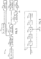
- a distributed motor control system 10 according to one embodiment of the invention is disclosed.
- An input voltage 11 is connected to a converter module 14 via a suitable disconnect 12, such as a fuse block or a circuit breaker.
- the input power 11 may be any suitable power supply such as three phase or single phase AC voltage, according to the application requirements.
- the converter module 14 converts the AC voltage into a DC voltage for distribution by the power management module 30.
- the converter module 14 and power management module 30 are mounted together in a control enclosure positioned near a machine or industrial process to be controlled. It is contemplated that the converter module 14 and the power management module 30 may either be separate modules or integrated as a single module without deviating from the scope of the invention.
- separate modules may be connected, for example, by electrical conductors or by a backplane connection in a rack-style enclosure.
- the connection may be used to transmit both power and control signals between modules.
- a DC voltage may be provided directly to the power management module 30 via the disconnect 12.
- the power management module 30 is connected in series with each power delivery module, also referred to herein as an inverter module 50.
- a cable 18 extends between the power management module 30 and a first of the inverter modules 50 as well as between subsequent inverter modules 50.
- the cable 18 includes all necessary connections to transmit, for example, power, reference commands, and/or network communications between each series connected inverter module 50.
- the cable may similarly include feedback signals from the inverter module 50 to the power management module 30.
- the cable 18 may include multiple conductors contained within a single jacket and appropriate shielding, separate conductors for each of the electrical connections, or a combination thereof.
- Each power delivery module 50 is mounted to a motor 15.
- Each motor 15 is mounted remotely from the control enclosure and connected to the machine or industrial process being controlled.
- the power delivery modules 50 include housings connected to the motor housing, for example, by bolts or which are, optionally, integrally formed with the corresponding motor housing.
- the voltage output to each motor 15 from the power delivery module 50 may be either a single or multi-phase AC output voltage according to the requirements of the motor 15.
- each motor 15 may include a position sensor 51 such as an encoder or a resolver providing a signal corresponding to the angular position of the motor 15.
- the converter module 14 includes a rectifier section 16, connected in series between the input voltage 11 and a DC bus 13, and a first DC bus capacitor 21 connected across the DC bus 13. It is understood that the DC bus capacitor 21 may be a single capacitor or multiple capacitors connected in parallel, in series, or a combination thereof.
- the rectifier section 16 may be either passive or active, where a passive rectifier utilizes electronic devices such as diodes, which require no control signals, and an active rectifier utilizes electronic devices including, but not limited to, transistors, thyristors, and silicon controlled rectifiers, which receive switching signals to turn on and/or off.
- the converter module 14 also includes a processor 26 and a memory device 27.
- the processor 26 and memory device 27 may each be a single electronic device or formed from multiple devices.
- the processor 26 and/or the memory device 27 may be integrated on a field programmable array (FPGA) or an application specific integrated circuit (ASIC).
- the processor 26 may send or receive signals to the rectifier section 16 as required by the application requirements.
- the processor 26 is also configured to communicate with external devices via an industrial network 28, including but not limited to, DeviceNet, ControlNet, or Ethernet/IP and its respective protocol.
- the processor 26 further communicates with other devices within the motor control system 10 via any suitable communications medium 29, such as a backplane connection or an industrial network, which may further include appropriate network cabling and routing devices.
- the power management module 30 is connected in series with the converter module 14. Electrical connections are established between the DC bus 13 of the converter module 14 and a DC bus 33 in the power management module 30 to transfer the DC bus voltage between modules. The connections may be made via a backplane connection, a power bus, or via a DC link cable 23. Alternately, if the two modules are integrated, the two DC busses, 13 and 33, may be combined into a single DC bus.
- the DC bus 33 includes a first voltage rail 32 and a second voltage rail 34. Each of the voltage rails, 32 or 34, are configured to conduct a DC voltage having a desired potential, according to application requirements.
- the first voltage rail 32 may have a DC voltage at a positive potential and the second voltage rail 34 may have a DC voltage at ground potential.
- the first voltage rail 32 may have a DC voltage at ground potential and the second voltage rail 34 may have a DC voltage at a negative potential
- the first voltage rail 32 may have a first DC voltage at a positive potential with respect to the ground potential and the second voltage rail 34 may have a second DC voltage at a negative potential with respect to the ground potential.
- the resulting DC voltage potential between the two voltage rails, 32 and 34 is the difference between the potential present on the first rail 32 and the second rail 34.
- the power management module 30 further includes a processor 40 and a memory device 42. It is contemplated that the processor 40 and memory device 42 may each be a single electronic device or formed from multiple devices. Optionally, the processor 40 and/or the memory device 42 may be integrated on a field programmable array (FPGA) or an application specific integrated circuit (ASIC).
- the processor 40 in the power management module 30 is in communication with the processor 26 in the converter module 14 via the communications medium 29.
- the communications medium 29 may be integrated into a backplane connection, integrated with the DC link cable 23 as a single cable, or provided as a separate network cable.
- the power management module 30 also includes at least one sensor 35 connected to the DC bus 33 and in communication with the processor 40. Each sensor 35 provides a signal to the processor corresponding to an operating condition, such as the amplitude of the voltage or current present on the DC bus 33.
- a DC link inductance 20 is mounted within the power management module 30 and connected in series with the DC link cable 23 to a power delivery module 50.
- the inductance 20 may be mounted external to the power management module 30.
- the DC link inductance includes a first inductor 22 connected in series between the positive voltage rails, 32 and 52, of the power management module 30 and the power delivery module 50, respectively, and a second inductor 24 connected in series between the negative voltage rails, 34 and 54, of the power management module 30 and the power delivery module 50, respectively.
- the DC bus 53 of the first power delivery module 50 is connected in series with the DC bus 33 of the power management module 30 and the DC bus 53 of subsequent power delivery modules 50 are connected in series with the DC bus 53 of the preceding power delivery module 50. Electrical connections are established between the DC bus 53 of each power delivery module 50 and its preceding module via a DC link cable 23 to transfer the DC bus voltage between modules. Similar to the DC bus 33 in the power management module 30, the DC bus 53 in the power delivery module 50 includes a first voltage rail 52 and a second voltage rail 54. Each of the voltage rails, 52 or 54, are configured such that they may conduct a DC voltage having the same potential as the voltage rails, 32 or 34, in the power management module 30.
- the power delivery module 50 further includes a processor 62 and a memory device 64. It is contemplated that the processor 62 and memory device 64 may each be a single electronic device or formed from multiple devices. Optionally, the processor 62 and/or the memory device 64 may be integrated on a field programmable array (FPGA) or an application specific integrated circuit (ASIC).
- the processor 62 in each power delivery module 50 is in communication with preceding module via the communications medium 29.
- the communications medium 29 and the DC link cable 23 define, at least in part, the cable 18 extending between modules.
- the power delivery module 50 also includes at least one sensor 55 connected to the DC bus 53 and in communication with the processor 40.
- Each sensor 55 provides a signal to the processor corresponding to an operating condition, such as the amplitude of the voltage or current present on the DC bus 33.
- At least one additional sensor 57 is connected to the output of the inverter section 60 and provides a signal to the processor 62 corresponding to the current in one of the phases of the AC output voltage to the motor 15.
- a DC bus capacitor 56 is connected between the positive and negative rails, 52 and 54, to reduce the magnitude of the ripple voltage present on the DC bus 53. It is understood that the DC bus capacitor 56 may be a single capacitor or multiple capacitors connected in parallel, in series, or a combination thereof.
- the magnitude of the voltage potential between the two voltage rails, 52 and 54, is generally about equal to the magnitude of the peak of the AC input voltage 11.
- the DC voltage on the DC bus 53 is converted to an AC voltage by an inverter section, 60. According to one embodiment of the invention, the inverter section 60 converts the DC voltage to a three-phase output voltage available at an output terminal 58 connected to the motor 15.
- the inverter section 60 includes multiple switches 71 which selectively connect one of the output phases to either the positive voltage rail 52 or the negative voltage rail 54.
- each switch 71 may include a transistor 72 and a diode 73 connected in parallel to the transistor 72.
- Each switch 71 receives a switching signal 75 to enable or disable conduction through the transistor 72 to selectively connect each phase of the output terminal 58 to either the positive voltage rail 52 or the negative voltage rail 54 of the DC bus 53.
- the converter module 14 receives an AC input voltage 11 and converts it to a DC voltage with the rectifier section 16.
- the AC input voltage 11 may be either a three phase or a single phase AC voltage.
- the processor 26 will receive signals from the active rectifier corresponding to, for example, amplitudes of the voltage and current on the AC input and/or the DC output.
- the processor 26 executes a program stored in memory 27 to generate switching signals to activate and/or deactivate the switches in the active rectifier, where the program includes a series of instructions executable on the processor 26.
- the switching signals may be generated such that power is transferred in either direction between the AC input and the DC output.
- the DC bus capacitor 21 connected across the DC bus 13 reduces the ripple voltage resulting from the voltage conversion.
- the DC voltage from the DC bus 13 of the converter module 14 is then provided to the DC bus 33 of the power management module 30.
- the processor 26 of the converter module 14 may further be configured to communicate with other external devices via the industrial network 28.
- the processor 26 may receive command signals from a user interface or from a control program executing, for example, on a programmable logic controller.
- the command signals may include, but are not limited to, speed, torque, or position commands used to control the rotation of each motor 15 in the distributed control system 10.
- the processor 26 may either pass the commands directly or execute a stored program to interpret the commands and subsequently transmit the commands to each inverter module 50.
- the processor 26 communicates with the processors, 40 or 62, of the power management module 30 and the inverter modules 50, directly or via a daisy chain topology and suitable communications media 29. Further, the processor 26 may either communicate using the same network protocol with which it received the commands via the industrial network 28 or convert the commands to a second protocol for transmission to subsequent modules, 30 or 50.
- the power management module 30 transfers the DC voltage and the control signals received from the converter module 14 to each power delivery module 50.
- the series connection of the DC bus 33 of the power management module 30 between the DC bus 13 of the converter module 14 and the DC bus 53 of the first power delivery, or inverter, module 50 establishes an electrical conduction path for the DC voltage between the converter module 14 and the inverter module 50.
- the DC bus capacitor 36 in the power management module 30 further reduces the ripple voltage on the DC bus resulting from voltage conversion.
- the power management module 30 and the converter module 14 may be integrated as a single unit, resulting in the combination of DC busses 13 and 33 into a single DC bus and the combination of DC bus capacitors, 21 and 36, into a single capacitance.
- the processor 40 receives a signal from at least one sensor 35 corresponding to the amplitude of the current and/or voltage present on the DC bus 33. Further, the processor 40 samples the amplitude of the current from the sensor 35 at a fast enough rate to monitor the amplitude of harmonic currents present on the DC bus 33.
- Each power delivery module 50 converts the DC voltage from the DC bus 53 to an AC voltage suitable to control operation of the motor 15 on which it is mounted.
- the processor 62 executes a program stored on a memory device 64.
- the processor 62 receives a reference signal via the communications medium 29 identifying the desired operation of the motor 15.
- the program includes a control module configured to control the motor 15 responsive to the reference signal and to feedback signals, including but not limited to signals from the voltage sensor 55, the current sensors 57, and the position sensor 51.
- the control module generates a desired voltage reference signal 104, see also Fig. 4 .
- the program further includes a switching module using, for example, pulse width modulation (PWM) to generate switching signals 75 to control the switches 71 responsive to the desired voltage reference signal 104.
- PWM pulse width modulation
- a segment of one phase of an AC voltage output according to an exemplary sine-triangle PWM modulation technique 100 is illustrated.
- a triangular waveform 102 is compared to the voltage reference 104 to generate switching signals 75.
- the switching signals 75 control the switches 71 that selectively connect or disconnect each phase of the output terminal 58 to either the positive voltage rail 52 or the negative voltage rail 54.
- One period of the triangular waveform 102 is defined by the switching period 106 of the PWM routine.
- the switching signal 75 is set high and, if the voltage reference 104 is less than the triangular waveform 102, the switching signal 75 is set low.
- the resulting output voltage 108 can be represented by a stepped waveform where the magnitude of the stepped waveform during each period 106 is the average value of the output voltage 108 during that period 106. The average value is determined by multiplying the magnitude of the DC voltage present on the DC bus 53 by the percentage of the period 106 that the switching signal 75 is set high. As the switching period 106 of the PWM routine decreases, the stepped output voltage 108 more accurately corresponds to the voltage reference 104.
- modulation techniques may also be used to generate the output voltage, such as space-vector or multi-level switching. Further, the modulation techniques may be implemented by comparing analog signals, as shown in Fig. 4 ; digital signals, such as a register being incremented up and down; or a combination thereof.
- the alternating connection and disconnection of the switches 71 to the DC bus 53 creates a ripple or fluctuation in the amplitude of the current on the DC bus 53.
- the amplitude and frequency of the ripple may be affected by many factors, including but not limited to the switching frequency and the modulation technique utilized.
- the modulation of the switches 71 may generate harmonic currents on the DC bus 53, for example, at the frequency, or multiples thereof, of the switching frequency.
- the switching routine may introduce harmonic currents at still other frequencies.
- the bus capacitor 56 on the power delivery module 50 helps reduce the ripple and the resulting harmonic currents present on the DC bus 53 in the power delivery module 50
- the physical size restraints from mounting the power delivery module 50 on the motor 15 restrict the amount of capacitance that may be included in the power delivery module 50, which, in turn, restricts the effectiveness of the capacitance 56 in reducing the harmonic currents.
- the DC link cable 23 connecting the DC bus 53 of the power delivery module 50 to the DC bus 33 of the power management module 30 may amplify any harmonic current generated by the switches 71 in the power delivery module 50.
- the DC link cable 23 introduces reactive components, for example a cable inductance, that are a function of the length of the DC link cable 23. Consequently, the amount the current is amplified is a function of the frequency of the harmonic current and the length of the DC link cable 23. Further, the distance the motors 15 and the power delivery modules 50 are located from the central enclosure may vary from one or two meters up to hundreds of meters.
- the inductance 20 mounted in series with the DC link cable 23 is configured to mitigate the harmonic currents present in the distributed motor control system 10.
- the magnitude of the inductance 20 is selected to attenuate harmonic content at the lowest frequency of harmonic current expected in the distributed motor control system 10.
- the harmonic currents on the DC link cable 23 are a function of the switching frequency, the modulation technique, the length of the DC link cable 23, and the size of the capacitance 56 present in the power delivery module 50.
- a modulation technique is selected which, for example, results in 2nd and 4th harmonic content being present on the DC link cable 23. If the switching frequency is selected at 2kHz, the resulting harmonic currents would have frequencies at 4 and 8 kHz.
- the magnitude of the inductance is selected such that the resulting DC link impedance attenuates the 4kHz harmonic current to an acceptable level.
- the harmonic currents generated are a function of the modulation technique implemented.
- the magnitude of the inductance is selected such that the resulting DC link impedance attenuates the harmonics generated from the modulation technique to an acceptable level.
- the attenuation results in about a 0 dB gain of the harmonic currents.
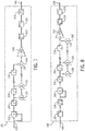
- the processor 40 in the power management module 30 receives an input signal corresponding to the amplitude of the DC link current 122.
- another processor in the motor control system 10 or a processor in an external processing device, including but not limited to a programmable logic controller (PLC) or a remote computer, may receive the signal.
- the input signal is sampled at a rate fast enough to measure the harmonic content present.
- the sampling frequency may be, for example, an order of magnitude greater than the highest expected harmonic current.
- the processor 40 is configured to read the signal from the sensor 35 corresponding to the amplitude of the current on the DC bus 33 at a rate fast enough to monitor the harmonic current present.
- a calibration module 124 applies an offset and scaling factor as needed according to the system requirements.
- the calibration module 124 may be implemented by a stored program executing on the processor 40 to add an offset to a digital value corresponding to the DC link current 122 or, optionally, may be implemented via an analog circuit which offsets the signal corresponding to the DC link current 122 prior to inputting the signal to the processor 40.
- the calibrated current signal 125 is used by an aggregate power calculation module 130 to determine the power consumed by the chain of power delivery modules 50 and motors 15 connected in series with the power management module 30.
- the calibrated current signal 125 is first sent through a low pass filter module 132 to eliminate the harmonic content.
- the bandwidth of the filter is preferably selected to output a signal corresponding to an average value of the DC link current having a response time comparable to the DC link voltage.
- the filtered current is passed through a down sampling block 134 such that the new frequency of the sampled current corresponds to the frequency at which the voltage on the DC bus 33 is sampled.
- the down sampling block 134 selects every nth data point from data sampled at a first frequency to obtain data at a second, lower frequency, where the value of "n" is selected according to the desired ratio between the original sampling frequency and the reduced sampling frequency.
- the down sampled current and the sampled DC voltage are passed through a multiplying block 136, which outputs the aggregate power consumed by the chain of power delivery modules 50.
- the aggregate power is finally passed through an anit-aliasing filter 138.
- the bandwidth of the anti-aliasing filter is selected as a function of the number and of the sampling frequency of the power delivery modules 50 connected to the DC bus 33.
- the calculated value of the aggregate power may be provided as an output 140, for example, to a display for monitoring by an operator.
- the aggregate power may be stored locally or remotely in a fixed or removable memory device or provided as an output 140 to another device for display or storage.
- the calibrated current signal 125 is also used by a first filter module, for example, a fast root mean square (rms) calculation module 150 to determine a time-averaged current signal which includes both the real and harmonic current components.
- a first filter module for example, a fast root mean square (rms) calculation module 150 to determine a time-averaged current signal which includes both the real and harmonic current components.
- the calibrated current signal 125 enters a multiplying block 152 which first multiplies the signal against itself, or squares the signal.
- the squared signal is passed through a series of delay blocks 154 and summing junctions 156 which form, for example, a 100-tap finite impulse response (FIR) filter.
- FIR finite impulse response
- other lengths of the FIR filter may be selected.
- the passband of the filter is selected such that the expected harmonic content is included in the rms calculation.
- the output of the FIR filter enters a gain block 158 to divide the output by the number of taps in the filter, resulting in the mean of the squared current.
- the mean of the squared current enters a square root block 160 which outputs the rms value of the sampled current.
- the fast rms calculation module 150 next passes the rms value through an anti-aliasing filter 162 and a down sampling block 164 and generates output 166 for subsequent calculations. It is contemplated that first filter module may be implemented using other suitable filters according to the application requirements.
- the output 166 of the fast rms calculation module 150 is provided as an input to a fast overload detection module 170 to determine whether the magnitude of the combined harmonic currents and DC current present on the the DC link cable 23 exceeds a predetermined threshold.
- the predetermined threshold is selected according to the application requirements and is a function of, for example, the size of the conductors in the DC link cable 23 or applicable industrial standards. If the total current on the DC link cable 23 exceeds the predetermined threshold, the processor 40 generates an output signal, which may be used, for example, to provide a visual or audio alert to an operator or to generate a message to be transmitted to another processor.
- the output 166 of the fast rms calculation module 150 is also provided as an input to a second filter module, for example, a slow rms calculation module 190.
- the input 166 is first passed through a low pass filter block 192 to filter out the harmonic content.
- the filtered content is subsequently down sampled 194 such that a slower processing task may operate on the sampled current.
- This filtered current corresponds to an average value of the current present on the DC bus 33.
- the filtered current signal enters a multiplying block 196 which first multiplies the signal against itself, or squares the signal.
- the squared signal is passed through a series of delay blocks 198 and summing junctions 200 which form, for example, a 100-tap finite impulse response (FIR) filter.
- FIR finite impulse response
- the output of the FIR filter enters a gain block 202 to divide the output by the number of taps in the filter, resulting in the mean of the squared current.
- the mean of the squared current enters a square root block 204 which outputs the rms value of the sampled current.
- the slow rms calculation module 190 next passes the rms value through an anti-aliasing filter 206 and generates output 208 for subsequent calculations. It is contemplated that second filter module may be implemented using other suitable filters according to the application requirements.
- the output 208 of the slow rms calculation module 190 is provided as an input to a bus utilization module 210 which monitors the rms current present on the DC bus 33.
- the rms current may be provided as an output, for example, to a display for monitoring by an operator.
- the rms current may be stored locally or remotely in a fixed or removable memory device or provided as a signal to another device for display or storage.
- the rms current may also be compared to a predetermined threshold.
- the predetermined threshold is selected according to the application requirements and is a function of, for example, the size of the conductors in the DC link cable 23 or applicable industrial standards. If the rms current on the DC bus 33 exceeds the predetermined threshold, the processor 40 generates an output signal, which may be used, for example, to provide a visual or audio alert to an operator or to generate a message to be transmitted to another processor.
- the output 208 of the slow rms calculation module 190 may also be utilized to select the DC link inductance 20 in the distributed motor control system 10.
- a remote processor such as an industrial controller or separate computer, may execute a program to simulate an input signal corresponding to the amplitude of the current present on the DC bus of the power management module.
- the simulated current signal includes the harmonic content expected within the system and is input to a model of the distributed motor control system 10 which simulates the damping characteristics of the DC link inductance 20.
- the output of the system model is then provided as the calibrated current signal 125 input to the blocks monitoring and managing the harmonic current.
- the output 208 of the slow rms calculation module 190 is then monitored and the value of the DC link inductance 20 within the system model is varied until the output 208, which corresponds to the bus utilization of the distributed motor control system 10 is below a predetermined threshold. Thus, a desired value of the DC link inductance 20 for use in the system may be determined.
Landscapes
- Engineering & Computer Science (AREA)
- Power Engineering (AREA)
- Physics & Mathematics (AREA)
- General Physics & Mathematics (AREA)
- Nonlinear Science (AREA)
- Mathematical Physics (AREA)
- Inverter Devices (AREA)
- Control Of Multiple Motors (AREA)
Claims (8)
- Verfahren zur Überwachung eines Stroms auf einem Gleichstrombus (33) eines Leistungsverwaltungsmoduls (30), das mit mindestens einem entfernten Wechselrichtermodul verbunden ist, wobei der Strom mindestens eine harmonische Komponente enthält, wobei das Verfahren die Schritte umfasst:Abtasten, mit einer ersten Abtastrate, eines Eingangssignals, das einer Amplitude des Stroms entspricht, der auf dem Gleichstrombus (33) des Leistungsverwaltungsmoduls vorhanden ist, wobei die erste Abtastrate ausreichend hoch ist, um die in dem Strom vorhandene harmonische Komponente zu überwachen, und eine Größenordnung höher ist als eine Frequenz eines höchsten erwarteten harmonischen Stroms;Ermitteln, in einem schnellen Berechnungsmodul für mittlere quadratische Wurzel, rms, (150), eines rms-Werts des Stroms (125), der mit der ersten Abtastrate abgetastet wird;in einem langsamen rms-Berechnungsmodul (190), Ausfiltern des harmonischen Anteils mit einem Tiefpassfilter (192) am Ausgang (166) des schnellen Berechnungsmoduls für mittlere quadratische Wurzel, rms, (150), und nachfolgend Abwärtsabtasten des ausgefilterten Anteils, der mit der ersten Abtastrate abgetastet wurde, auf eine zweite Abtastrate, die niedriger ist als die erste Abtastrate;Zuführen des Ausgangssignals (208) des langsamen rms-Berechnungsmoduls als Eingangssignal für ein Busauslastungsmodul (210), das den rms-Wert des Gleichstroms, der auf dem Gleichstrombus (33) vorhanden ist, überwacht; undErzeugen eines Ausgangssignals, das den rms-Wert des Gleichstroms, der auf dem Gleichstrombus des Leistungsverwaltungsmoduls vorhanden ist, entspricht, als eine Funktion des rms-Werts des Gleichstroms, der mit der zweiten Abtastrate mittels des Busauslastungsmoduls (210) abgetastet wird.
- Verfahren nach Anspruch 1, das ferner die Schritte umfasst:Vergleichen in einem schnellen Überlasterfassungsmodul (170) des rms-Werts des mit der ersten Abtastrate abgetasteten Stroms mit einem ersten Schwellenwert;Erzeugen, mit dem schnellen Überlasterfassungsmodul, eines ersten Überlastsignals, wenn der rms-Wert des mit der ersten Abtastrate abgetasteten Stroms größer ist als der erste Schwellenwert und Zurücksetzen des ersten Überlastsignals, wenn der rms-Wert des mit der ersten Abtastrate abgetasteten Stroms kleiner ist als der erste Schwellenwert;Vergleichen, in dem Busauslastungsmodul, des rms-Werts des mit der zweiten Abtastrate abgetasteten Gleichstroms mit einem zweiten Schwellenwert; undErzeugen eines zweiten Ausgangssignals, das einer Auslastungsrate des Gleichstrombusses entspricht, wenn der rms-Wert des Gleichstroms, der mit der zweiten Abtastrate abgetastet wird, größer ist als der zweite Schwellenwert, und Zurücksetzen des zweiten Überlastsignals, wenn der rms-Wert des Gleichstroms, der mit der zweiten Abtastrate abgetastet wird, kleiner ist als der zweite Schwellenwert.
- Verfahren nach Anspruch 2, wobei das Leistungsverwaltungsmodul mit einer entfernten Industriesteuerung in Verbindung ist, und wobei nach dem Abtasten des Eingangssignals das Verfahren ferner den Schritt umfasst: Übertragen der abgetasteten Amplitude des Stroms, der auf dem Gleichstrombus vorhanden ist, zu der entfernten Industriesteuerung, und wobei die entfernte Industriesteuerung einen Prozessor aufweist, der ausgebildet ist, die verbleibenden Schritte auszuführen.
- Verfahren nach Anspruch 1, wobei:jedes entfernte Wechselrichtermodul ein Schaltmodul und einen Gleichstrombus aufweist, wobei der Gleichstrombus des Wechselrichtermoduls mit dem Gleichstrombus des Leistungsverwaltungsmoduls durch einen Leiter verbunden ist,jedes entfernte Wechselrichtermodul an einem Motor montiert ist, unddas Verfahren ferner den Umfangsschritt umfasst: selektives Verbinden des Gleichstrombusses des Wechselrichtermoduls mit mindestens einem Leiter eines Stators, der in dem Motor vorhanden ist, mit einer vorbestimmten Schaltfrequenz, wobei:mindestens ein harmonischer Strom als Funktion des selektiven Verbindens des Gleichstrombusses erzeugt wird,die harmonischen Ströme von dem Leiter, der den Gleichstrombus des mindestens einen entfernten Wechselrichtermoduls mit dem Gleichstrombus eines Leistungsverwaltungsmoduls verbindet, übertragen werden.
- Verfahren nach Anspruch 4, wobei:eine Gleichstromverbindungsinduktivität zwischen dem Gleichstrombus des Leistungsverwaltungsmoduls und dem Gleichstrombus des mindestens einen entfernten Wechselrichtermoduls in Reihe geschaltet ist, undder Stromsensor den Strom in Reihe zwischen dem Gleichstrombus des Leistungsverwaltungsmoduls und der Gleichstromverbindungsinduktivität abtastet.
- Verfahren nach Anspruch 5, wobei die zweite Abtastrate niedriger ist als die Frequenz des mindestens einen harmonischen Stroms und höher ist als die Frequenz eines Servosteuermoduls, das ausgebildet ist, in einem Prozessor des Wechselrichtermoduls ausgeführt zu werden.
- System zur Überwachung von Strom in mehreren Motoren (15), die in einer Industrieanlage oder einem Prozess verteilt sind, wobei der Strom mindestens eine harmonische Komponente enthält, wobei das System umfasst:ein Umwandlungsmodul (14), das ausgebildet ist, ein Wechselstromspannungseingangssignal zu empfangen und das Wechselstromspannungseingangssignal in eine Gleichstromspannung umzuwandeln;einen lokalen Gleichstrombus (33), der die Gleichstromspannung aus dem Umwandlungsmodul empfängt;eine erste Kapazität (36), die an dem lokalen Gleichstrombus angeschlossen ist;mehrere Motorsteuermodule (50), wobei jedes Motorsteuermodul an einem der Motore (15) montiert ist, wobei das Motorsteuermodul ferner umfasst:einen entfernten Gleichstrombus (53), der über mindestens ein Gleichstromverbindungskabel (23) mit dem lokalen Gleichstrombus verbunden ist,eine zweite Kapazität (56), die kleiner als die erste Kapazität ist und an dem entfernten Gleichstrombus angeschlossen ist, undeinen Wechselrichterblock (60) mit mehreren Schaltern, der ausgebildet ist, die Gleichstromspannung in eine Wechselstromspannung, die zur Ansteuerung des Motors geeignet ist, umzuwandeln;eine Induktivität (20), die zwischen dem lokalen Gleichstrombus und dem entfernten Gleichstrombus eines ersten der Motorsteuermodule in Reihe geschaltet ist;eine Stromerfassungseinrichtung (35), die ausgebildet ist, den auf dem lokalen Gleichstrombus vorhandenen Strom mit einer ersten Abtastfrequenz abzutasten und ein entsprechendes Signal zu erzeugen, wobei die erste Abtastfrequenz ausreichend hoch ist, um die mindestens eine harmonische Komponente, die in dem Strom vorhanden ist, zu überwachen, und eine Größenordnung höher ist als eine Frequenz eines höchsten erwarteten harmonischen Stroms;ein schnelles Berechnungsmodul für mittlere quadratische Wurzel, rms, (150), das ausgebildet ist, einen rms-Wert der Signale aus der Stromerfassungseinrichtung zu ermitteln;ein langsames rms-Berechnungsmodul (190), das ausgebildet ist, mit einem Tiefpassfilter (192) den harmonischen Anteil in dem Ausgangssignal (166) des schnellen Berechnungsmoduls für mittlere quadratische Wurzel, rms, (150) auszufiltern und nachfolgend den ausgefilterten Anteil, der mit der ersten Abtastrate abgetastet ist, auf eine zweite Abtastrate, die niedriger als die erste Abtastrate ist, abwärts abzutasten; undein Busauslastungsmodul (210), das ausgebildet ist, ein Ausgangssignal entsprechend zu dem rms-Wert des Gleichstroms, der auf dem Gleichstrombus des Leistungsverwaltungsmoduls vorhanden ist, als eine Funktion des rms-Werts des Gleichstroms, der mit der zweiten Abtastrate abgetastet wird, zu erzeugen.
- System nach Anspruch 7, wobei:jedes der Gleichstromverbindungskabel einen ersten und einen zweiten elektrischen Leiter enthält,die Induktivität eine erste und eine zweite Induktivität umfasst, die entsprechend mit dem ersten und dem zweiten elektrischen Leiter in Reihe geschaltet sind,das Motorsteuermodul ferner umfasst:einen Ausgang, der ausgebildet ist, die Wechselstromspannung zu dem Motor zu führen; undeinen Prozessor, der ausgebildet ist, eine Reihe von Befehlen auszuführen, um mehrere Schaltsignale mit vorbestimmter Frequenz zu erzeugen, wobei die Schalter in dem Wechselrichtermodul durch die Schaltsignale so gesteuert sind, dass selektiv der Gleichstrombus mit dem Ausgang verbunden wird, und wobei die Größe der Induktivität eine Funktion der vorbestimmten Frequenz ist.
Applications Claiming Priority (1)
| Application Number | Priority Date | Filing Date | Title |
|---|---|---|---|
| US13/295,690 US8766584B2 (en) | 2011-11-14 | 2011-11-14 | System and method for managing DC link switching harmonics |
Publications (3)
| Publication Number | Publication Date |
|---|---|
| EP2592736A2 EP2592736A2 (de) | 2013-05-15 |
| EP2592736A3 EP2592736A3 (de) | 2015-07-29 |
| EP2592736B1 true EP2592736B1 (de) | 2020-06-24 |
Family
ID=47257493
Family Applications (1)
| Application Number | Title | Priority Date | Filing Date |
|---|---|---|---|
| EP12192650.5A Active EP2592736B1 (de) | 2011-11-14 | 2012-11-14 | System und Verfahren zum Überwachen von Schaltharmonischen in einem Gleichstromzwischenkreis |
Country Status (2)
| Country | Link |
|---|---|
| US (2) | US8766584B2 (de) |
| EP (1) | EP2592736B1 (de) |
Families Citing this family (17)
| Publication number | Priority date | Publication date | Assignee | Title |
|---|---|---|---|---|
| NO332768B1 (no) * | 2009-12-16 | 2013-01-14 | Smartmotor As | System for drift av langstrakte elektriske maskiner |
| FR2982092B1 (fr) * | 2011-11-02 | 2015-01-02 | Valeo Systemes De Controle Moteur | Module de puissance et dispositif electrique pour l'alimentation et la charge combinees respectivement d'un accumulateur et d'un moteur |
| US9318991B2 (en) * | 2013-04-11 | 2016-04-19 | The Boeing Company | Electric motor frequency modulation system |
| DE102014203781A1 (de) * | 2014-02-28 | 2015-09-03 | Schmidhauser Ag | Frequenzumrichter |
| US9882421B2 (en) * | 2015-05-14 | 2018-01-30 | Rockwell Automation Technologies, Inc. | Method and apparatus for increasing current capacity of a distributed drive system |
| US9419642B1 (en) * | 2015-06-11 | 2016-08-16 | Analog Devices, Inc. | Ultra low power dual quantizer architecture for oversampling delta-sigma modulator |
| JP6711117B2 (ja) * | 2016-04-28 | 2020-06-17 | 富士電機株式会社 | 多軸ドライブ装置およびサーボアンプ |
| US10914484B2 (en) * | 2016-04-29 | 2021-02-09 | Regal Beloit America, Inc. | System, motor controller and associated method |
| US10375216B2 (en) | 2017-09-29 | 2019-08-06 | Rockwell Automation Technologies, Inc. | Method and apparatus for communication in a motor drive application |
| JP2019093459A (ja) * | 2017-11-20 | 2019-06-20 | セイコーエプソン株式会社 | ロボット |
| US10644635B2 (en) | 2018-06-26 | 2020-05-05 | Rockwell Automation Technologies, Inc. | Systems and methods for motor drive cable characteristics identification and compensation therefor |
| US11863105B2 (en) * | 2018-07-25 | 2024-01-02 | Abb Schweiz Ag | Method and control system for controlling an electric motor |
| JP7472462B2 (ja) * | 2019-10-11 | 2024-04-23 | オムロン株式会社 | サーボdc給電システム及びモータ制御装置 |
| US11333690B2 (en) | 2019-12-16 | 2022-05-17 | Schneider Electric USA, Inc. | Current measurement compensation for harmonics |
| US11482853B2 (en) * | 2020-08-17 | 2022-10-25 | Infineon Technologies Austria Ag | Power delivery control and over current protection |
| WO2022094402A1 (en) * | 2020-10-30 | 2022-05-05 | Velocity Magnetics, Inc. | Method, system, and computer program product for an insulated-gate bipolar transistor (igbt) rectifier for charging ultra-capacitors |
| US20230408601A1 (en) * | 2022-06-17 | 2023-12-21 | Honeywell Limited | Fault detection in a power distribution system providing high voltage direct current through multiple channels with a floating ground |
Citations (2)
| Publication number | Priority date | Publication date | Assignee | Title |
|---|---|---|---|---|
| EP0713279A1 (de) * | 1994-11-18 | 1996-05-22 | Eaton Corporation | Vorrichtung zum Schutz und zur Leistungsmessung eines elektrischen Wechselspannungssystems mittels Multifunktionsabtasttechnik |
| US20090012728A1 (en) * | 2005-01-27 | 2009-01-08 | Electro Industries/Gauge Tech. | System and Method for Multi-Rate Concurrent Waveform Capture and Storage for Power Quality Metering |
Family Cites Families (15)
| Publication number | Priority date | Publication date | Assignee | Title |
|---|---|---|---|---|
| JPS605151B2 (ja) | 1978-04-05 | 1985-02-08 | 株式会社日立製作所 | 多重化電流形インバ−タの制御方法 |
| US4508996A (en) * | 1980-06-23 | 1985-04-02 | Brigham Young University | High frequency supply system for gas discharge lamps and electronic ballast therefor |
| DE4330537B4 (de) * | 1993-09-09 | 2006-06-01 | Robert Bosch Gmbh | Frequenzumrichter und Verfahren zu seinem Betrieb |
| EP0809349B1 (de) * | 1996-05-22 | 2001-07-18 | STMicroelectronics S.r.l. | Volldigitalsteuerungssystem für einen bürstenlosen Motor mit aus einem Digitalspeicher gelesenen Spannungs- bzw. Stromprofil |
| US6198613B1 (en) * | 1998-12-23 | 2001-03-06 | Hamilton Sundstrand Corporation | Method and apparatus for distributing alternating electrical current to motors via a direct current bus |
| US6404655B1 (en) * | 1999-12-07 | 2002-06-11 | Semikron, Inc. | Transformerless 3 phase power inverter |
| US6295216B1 (en) | 2000-04-06 | 2001-09-25 | Powerware Corporation | Power supply apparatus with selective rectifier harmonic input current suppression and methods of operation thereof |
| DE10218669B4 (de) | 2002-04-26 | 2015-04-02 | Daimler Ag | Brennstoffzellensystem und Verfahren zur Spannungsüberwachung für ein Brennstoffzellensystem |
| JP3851617B2 (ja) * | 2003-05-27 | 2006-11-29 | ファナック株式会社 | モータ駆動装置 |
| US7164242B2 (en) | 2004-02-27 | 2007-01-16 | York International Corp. | Variable speed drive for multiple loads |
| US7348758B2 (en) * | 2005-10-26 | 2008-03-25 | International Rectifier Corporation | Audible noise reduction for single current shunt platform |
| US7392143B2 (en) * | 2006-03-14 | 2008-06-24 | The University Of Texas System Board Of Regents | Monitoring and fault diagnosis of single-and multi-converter power systems |
| US7800333B2 (en) * | 2007-03-20 | 2010-09-21 | International Rectifier Corporation | Audible noise reduction for single current shunt platform |
| DE102008022617A1 (de) | 2008-05-07 | 2009-11-19 | Siemens Aktiengesellschaft | Windenergiepark mit einer Vielzahl von Windenergieanlagen |
| JP2011147300A (ja) | 2010-01-15 | 2011-07-28 | Merstech Inc | 電力逆変換装置及び電力逆変換方法 |
-
2011
- 2011-11-14 US US13/295,690 patent/US8766584B2/en active Active
-
2012
- 2012-11-14 EP EP12192650.5A patent/EP2592736B1/de active Active
-
2014
- 2014-06-10 US US14/300,396 patent/US9270210B2/en not_active Expired - Fee Related
Patent Citations (2)
| Publication number | Priority date | Publication date | Assignee | Title |
|---|---|---|---|---|
| EP0713279A1 (de) * | 1994-11-18 | 1996-05-22 | Eaton Corporation | Vorrichtung zum Schutz und zur Leistungsmessung eines elektrischen Wechselspannungssystems mittels Multifunktionsabtasttechnik |
| US20090012728A1 (en) * | 2005-01-27 | 2009-01-08 | Electro Industries/Gauge Tech. | System and Method for Multi-Rate Concurrent Waveform Capture and Storage for Power Quality Metering |
Also Published As
| Publication number | Publication date |
|---|---|
| US20140285120A1 (en) | 2014-09-25 |
| US8766584B2 (en) | 2014-07-01 |
| US20130119902A1 (en) | 2013-05-16 |
| EP2592736A3 (de) | 2015-07-29 |
| EP2592736A2 (de) | 2013-05-15 |
| US9270210B2 (en) | 2016-02-23 |
Similar Documents
| Publication | Publication Date | Title |
|---|---|---|
| EP2592736B1 (de) | System und Verfahren zum Überwachen von Schaltharmonischen in einem Gleichstromzwischenkreis | |
| US8860335B2 (en) | System for managing DC link switching harmonics | |
| EP2408099B1 (de) | Motorantriebssystem mit parallel geschalteten Stromrichtern | |
| CN104880965A (zh) | 加热控制和/或调节的功率模块和接口模块和模块化系统 | |
| WO2023183491A1 (en) | Communication systems and synchronization techniques for energy storage systems | |
| US10594247B2 (en) | Output module of a drive control system | |
| EP3483678A2 (de) | Verfahren und vorrichtung zur online-simulation komplexer bewegungssysteme | |
| EP4109738A1 (de) | System und verfahren zur bahnformung für machbare bewegungsbefehle | |
| US9148042B2 (en) | Method and apparatus for detection of drive misconfiguration in a multi-axis configuration | |
| US11804789B2 (en) | System and method for protecting an electrical load of a drive system | |
| EP4216426B1 (de) | System und verfahren zur bestimmung einer zyklischen störung in einem industriellen steuerungssystem | |
| CN103503317A (zh) | 具有至少三个监视输入的波上点控制器 | |
| Galketiya et al. | Novel communication system for scada tied smart inverter for vietnam | |
| CN103701092A (zh) | 一种直流电气系统绝缘电阻检测与接地保护装置 | |
| EP3736933B1 (de) | Verfahren und vorrichtung zur verteilung von gleichstrom-bus-spannung und steuerspannung über gemeinsame leiter in einem verteilten gleichstrombussystem | |
| US12531496B2 (en) | System and method for reducing energy loss from multiple inverters utilizing a shared DC bus | |
| CN203027176U (zh) | 一种可移动的集成化应急励磁装置 | |
| Krasnoperov et al. | Research and Development of Semiconductor Regulators Automatic Control Software-Hardware Complex (SHC) to Voltage Regulation and Improve Reliability and Power Quality for Distribution Networks 10/0.4 kV | |
| KR101884120B1 (ko) | 고속 스위칭이 가능한 이중화 통신모듈 및 이를 이용한 보호 계전 시스템 | |
| CN104730380B (zh) | 用于发电机组的滤波器的故障检测装置、方法及系统 | |
| Staudt et al. | Development of a new 1000 V/1 MVA IGBT 3L-NPC-VSC PEBB type 2 with independent modulation, DC-link balancing and short-circuit protection | |
| Avery | VFDs from the inside out: variable frequency drive (VFD) vocabulary words: These 50 terms can help properly apply VFDs. | |
| DK177665B1 (en) | Photovoltaic Power Plant | |
| KR20170099270A (ko) | 초고압 직류 송전 시스템에서의 제어장치 및 이의 제어방법 | |
| CN117999721A (zh) | 供电装置 |
Legal Events
| Date | Code | Title | Description |
|---|---|---|---|
| PUAI | Public reference made under article 153(3) epc to a published international application that has entered the european phase |
Free format text: ORIGINAL CODE: 0009012 |
|
| AK | Designated contracting states |
Kind code of ref document: A2 Designated state(s): AL AT BE BG CH CY CZ DE DK EE ES FI FR GB GR HR HU IE IS IT LI LT LU LV MC MK MT NL NO PL PT RO RS SE SI SK SM TR |
|
| AX | Request for extension of the european patent |
Extension state: BA ME |
|
| PUAL | Search report despatched |
Free format text: ORIGINAL CODE: 0009013 |
|
| AK | Designated contracting states |
Kind code of ref document: A3 Designated state(s): AL AT BE BG CH CY CZ DE DK EE ES FI FR GB GR HR HU IE IS IT LI LT LU LV MC MK MT NL NO PL PT RO RS SE SI SK SM TR |
|
| AX | Request for extension of the european patent |
Extension state: BA ME |
|
| RIC1 | Information provided on ipc code assigned before grant |
Ipc: G01R 21/133 20060101ALI20150623BHEP Ipc: H02M 1/15 20060101AFI20150623BHEP Ipc: H02M 5/458 20060101ALI20150623BHEP |
|
| 17P | Request for examination filed |
Effective date: 20160129 |
|
| RBV | Designated contracting states (corrected) |
Designated state(s): AL AT BE BG CH CY CZ DE DK EE ES FI FR GB GR HR HU IE IS IT LI LT LU LV MC MK MT NL NO PL PT RO RS SE SI SK SM TR |
|
| STAA | Information on the status of an ep patent application or granted ep patent |
Free format text: STATUS: EXAMINATION IS IN PROGRESS |
|
| 17Q | First examination report despatched |
Effective date: 20180607 |
|
| REG | Reference to a national code |
Ref country code: DE Ref legal event code: R079 Ref document number: 602012070858 Country of ref document: DE Free format text: PREVIOUS MAIN CLASS: H02M0001150000 Ipc: H02M0001000000 |
|
| RIC1 | Information provided on ipc code assigned before grant |
Ipc: H02M 1/15 20060101ALI20191125BHEP Ipc: G01R 31/42 20060101ALI20191125BHEP Ipc: H02M 5/458 20060101ALI20191125BHEP Ipc: G01R 19/25 20060101ALI20191125BHEP Ipc: H02M 1/00 20060101AFI20191125BHEP Ipc: G01R 23/20 20060101ALI20191125BHEP |
|
| GRAP | Despatch of communication of intention to grant a patent |
Free format text: ORIGINAL CODE: EPIDOSNIGR1 |
|
| STAA | Information on the status of an ep patent application or granted ep patent |
Free format text: STATUS: GRANT OF PATENT IS INTENDED |
|
| INTG | Intention to grant announced |
Effective date: 20200108 |
|
| GRAJ | Information related to disapproval of communication of intention to grant by the applicant or resumption of examination proceedings by the epo deleted |
Free format text: ORIGINAL CODE: EPIDOSDIGR1 |
|
| STAA | Information on the status of an ep patent application or granted ep patent |
Free format text: STATUS: EXAMINATION IS IN PROGRESS |
|
| GRAR | Information related to intention to grant a patent recorded |
Free format text: ORIGINAL CODE: EPIDOSNIGR71 |
|
| GRAS | Grant fee paid |
Free format text: ORIGINAL CODE: EPIDOSNIGR3 |
|
| STAA | Information on the status of an ep patent application or granted ep patent |
Free format text: STATUS: GRANT OF PATENT IS INTENDED |
|
| GRAA | (expected) grant |
Free format text: ORIGINAL CODE: 0009210 |
|
| STAA | Information on the status of an ep patent application or granted ep patent |
Free format text: STATUS: THE PATENT HAS BEEN GRANTED |
|
| INTC | Intention to grant announced (deleted) | ||
| INTG | Intention to grant announced |
Effective date: 20200514 |
|
| AK | Designated contracting states |
Kind code of ref document: B1 Designated state(s): AL AT BE BG CH CY CZ DE DK EE ES FI FR GB GR HR HU IE IS IT LI LT LU LV MC MK MT NL NO PL PT RO RS SE SI SK SM TR |
|
| REG | Reference to a national code |
Ref country code: GB Ref legal event code: FG4D |
|
| REG | Reference to a national code |
Ref country code: CH Ref legal event code: EP |
|
| REG | Reference to a national code |
Ref country code: AT Ref legal event code: REF Ref document number: 1284875 Country of ref document: AT Kind code of ref document: T Effective date: 20200715 |
|
| REG | Reference to a national code |
Ref country code: DE Ref legal event code: R096 Ref document number: 602012070858 Country of ref document: DE |
|
| REG | Reference to a national code |
Ref country code: IE Ref legal event code: FG4D |
|
| PG25 | Lapsed in a contracting state [announced via postgrant information from national office to epo] |
Ref country code: LT Free format text: LAPSE BECAUSE OF FAILURE TO SUBMIT A TRANSLATION OF THE DESCRIPTION OR TO PAY THE FEE WITHIN THE PRESCRIBED TIME-LIMIT Effective date: 20200624 Ref country code: SE Free format text: LAPSE BECAUSE OF FAILURE TO SUBMIT A TRANSLATION OF THE DESCRIPTION OR TO PAY THE FEE WITHIN THE PRESCRIBED TIME-LIMIT Effective date: 20200624 Ref country code: GR Free format text: LAPSE BECAUSE OF FAILURE TO SUBMIT A TRANSLATION OF THE DESCRIPTION OR TO PAY THE FEE WITHIN THE PRESCRIBED TIME-LIMIT Effective date: 20200925 Ref country code: NO Free format text: LAPSE BECAUSE OF FAILURE TO SUBMIT A TRANSLATION OF THE DESCRIPTION OR TO PAY THE FEE WITHIN THE PRESCRIBED TIME-LIMIT Effective date: 20200924 Ref country code: FI Free format text: LAPSE BECAUSE OF FAILURE TO SUBMIT A TRANSLATION OF THE DESCRIPTION OR TO PAY THE FEE WITHIN THE PRESCRIBED TIME-LIMIT Effective date: 20200624 |
|
| REG | Reference to a national code |
Ref country code: LT Ref legal event code: MG4D |
|
| PG25 | Lapsed in a contracting state [announced via postgrant information from national office to epo] |
Ref country code: LV Free format text: LAPSE BECAUSE OF FAILURE TO SUBMIT A TRANSLATION OF THE DESCRIPTION OR TO PAY THE FEE WITHIN THE PRESCRIBED TIME-LIMIT Effective date: 20200624 Ref country code: RS Free format text: LAPSE BECAUSE OF FAILURE TO SUBMIT A TRANSLATION OF THE DESCRIPTION OR TO PAY THE FEE WITHIN THE PRESCRIBED TIME-LIMIT Effective date: 20200624 Ref country code: HR Free format text: LAPSE BECAUSE OF FAILURE TO SUBMIT A TRANSLATION OF THE DESCRIPTION OR TO PAY THE FEE WITHIN THE PRESCRIBED TIME-LIMIT Effective date: 20200624 Ref country code: BG Free format text: LAPSE BECAUSE OF FAILURE TO SUBMIT A TRANSLATION OF THE DESCRIPTION OR TO PAY THE FEE WITHIN THE PRESCRIBED TIME-LIMIT Effective date: 20200924 |
|
| REG | Reference to a national code |
Ref country code: NL Ref legal event code: MP Effective date: 20200624 |
|
| REG | Reference to a national code |
Ref country code: AT Ref legal event code: MK05 Ref document number: 1284875 Country of ref document: AT Kind code of ref document: T Effective date: 20200624 |
|
| PG25 | Lapsed in a contracting state [announced via postgrant information from national office to epo] |
Ref country code: NL Free format text: LAPSE BECAUSE OF FAILURE TO SUBMIT A TRANSLATION OF THE DESCRIPTION OR TO PAY THE FEE WITHIN THE PRESCRIBED TIME-LIMIT Effective date: 20200624 Ref country code: AL Free format text: LAPSE BECAUSE OF FAILURE TO SUBMIT A TRANSLATION OF THE DESCRIPTION OR TO PAY THE FEE WITHIN THE PRESCRIBED TIME-LIMIT Effective date: 20200624 |
|
| PG25 | Lapsed in a contracting state [announced via postgrant information from national office to epo] |
Ref country code: RO Free format text: LAPSE BECAUSE OF FAILURE TO SUBMIT A TRANSLATION OF THE DESCRIPTION OR TO PAY THE FEE WITHIN THE PRESCRIBED TIME-LIMIT Effective date: 20200624 Ref country code: CZ Free format text: LAPSE BECAUSE OF FAILURE TO SUBMIT A TRANSLATION OF THE DESCRIPTION OR TO PAY THE FEE WITHIN THE PRESCRIBED TIME-LIMIT Effective date: 20200624 Ref country code: ES Free format text: LAPSE BECAUSE OF FAILURE TO SUBMIT A TRANSLATION OF THE DESCRIPTION OR TO PAY THE FEE WITHIN THE PRESCRIBED TIME-LIMIT Effective date: 20200624 Ref country code: PT Free format text: LAPSE BECAUSE OF FAILURE TO SUBMIT A TRANSLATION OF THE DESCRIPTION OR TO PAY THE FEE WITHIN THE PRESCRIBED TIME-LIMIT Effective date: 20201026 Ref country code: IT Free format text: LAPSE BECAUSE OF FAILURE TO SUBMIT A TRANSLATION OF THE DESCRIPTION OR TO PAY THE FEE WITHIN THE PRESCRIBED TIME-LIMIT Effective date: 20200624 Ref country code: AT Free format text: LAPSE BECAUSE OF FAILURE TO SUBMIT A TRANSLATION OF THE DESCRIPTION OR TO PAY THE FEE WITHIN THE PRESCRIBED TIME-LIMIT Effective date: 20200624 Ref country code: SM Free format text: LAPSE BECAUSE OF FAILURE TO SUBMIT A TRANSLATION OF THE DESCRIPTION OR TO PAY THE FEE WITHIN THE PRESCRIBED TIME-LIMIT Effective date: 20200624 Ref country code: EE Free format text: LAPSE BECAUSE OF FAILURE TO SUBMIT A TRANSLATION OF THE DESCRIPTION OR TO PAY THE FEE WITHIN THE PRESCRIBED TIME-LIMIT Effective date: 20200624 |
|
| PG25 | Lapsed in a contracting state [announced via postgrant information from national office to epo] |
Ref country code: PL Free format text: LAPSE BECAUSE OF FAILURE TO SUBMIT A TRANSLATION OF THE DESCRIPTION OR TO PAY THE FEE WITHIN THE PRESCRIBED TIME-LIMIT Effective date: 20200624 Ref country code: SK Free format text: LAPSE BECAUSE OF FAILURE TO SUBMIT A TRANSLATION OF THE DESCRIPTION OR TO PAY THE FEE WITHIN THE PRESCRIBED TIME-LIMIT Effective date: 20200624 Ref country code: IS Free format text: LAPSE BECAUSE OF FAILURE TO SUBMIT A TRANSLATION OF THE DESCRIPTION OR TO PAY THE FEE WITHIN THE PRESCRIBED TIME-LIMIT Effective date: 20201024 |
|
| REG | Reference to a national code |
Ref country code: DE Ref legal event code: R097 Ref document number: 602012070858 Country of ref document: DE |
|
| PG25 | Lapsed in a contracting state [announced via postgrant information from national office to epo] |
Ref country code: DK Free format text: LAPSE BECAUSE OF FAILURE TO SUBMIT A TRANSLATION OF THE DESCRIPTION OR TO PAY THE FEE WITHIN THE PRESCRIBED TIME-LIMIT Effective date: 20200624 |
|
| PLBE | No opposition filed within time limit |
Free format text: ORIGINAL CODE: 0009261 |
|
| STAA | Information on the status of an ep patent application or granted ep patent |
Free format text: STATUS: NO OPPOSITION FILED WITHIN TIME LIMIT |
|
| 26N | No opposition filed |
Effective date: 20210325 |
|
| PG25 | Lapsed in a contracting state [announced via postgrant information from national office to epo] |
Ref country code: MC Free format text: LAPSE BECAUSE OF FAILURE TO SUBMIT A TRANSLATION OF THE DESCRIPTION OR TO PAY THE FEE WITHIN THE PRESCRIBED TIME-LIMIT Effective date: 20200624 |
|
| REG | Reference to a national code |
Ref country code: CH Ref legal event code: PL |
|
| PG25 | Lapsed in a contracting state [announced via postgrant information from national office to epo] |
Ref country code: LU Free format text: LAPSE BECAUSE OF NON-PAYMENT OF DUE FEES Effective date: 20201114 |
|
| REG | Reference to a national code |
Ref country code: BE Ref legal event code: MM Effective date: 20201130 |
|
| PG25 | Lapsed in a contracting state [announced via postgrant information from national office to epo] |
Ref country code: CH Free format text: LAPSE BECAUSE OF NON-PAYMENT OF DUE FEES Effective date: 20201130 Ref country code: SI Free format text: LAPSE BECAUSE OF FAILURE TO SUBMIT A TRANSLATION OF THE DESCRIPTION OR TO PAY THE FEE WITHIN THE PRESCRIBED TIME-LIMIT Effective date: 20200624 Ref country code: LI Free format text: LAPSE BECAUSE OF NON-PAYMENT OF DUE FEES Effective date: 20201130 |
|
| PG25 | Lapsed in a contracting state [announced via postgrant information from national office to epo] |
Ref country code: IE Free format text: LAPSE BECAUSE OF NON-PAYMENT OF DUE FEES Effective date: 20201114 |
|
| PG25 | Lapsed in a contracting state [announced via postgrant information from national office to epo] |
Ref country code: TR Free format text: LAPSE BECAUSE OF FAILURE TO SUBMIT A TRANSLATION OF THE DESCRIPTION OR TO PAY THE FEE WITHIN THE PRESCRIBED TIME-LIMIT Effective date: 20200624 Ref country code: MT Free format text: LAPSE BECAUSE OF FAILURE TO SUBMIT A TRANSLATION OF THE DESCRIPTION OR TO PAY THE FEE WITHIN THE PRESCRIBED TIME-LIMIT Effective date: 20200624 Ref country code: CY Free format text: LAPSE BECAUSE OF FAILURE TO SUBMIT A TRANSLATION OF THE DESCRIPTION OR TO PAY THE FEE WITHIN THE PRESCRIBED TIME-LIMIT Effective date: 20200624 |
|
| PG25 | Lapsed in a contracting state [announced via postgrant information from national office to epo] |
Ref country code: MK Free format text: LAPSE BECAUSE OF FAILURE TO SUBMIT A TRANSLATION OF THE DESCRIPTION OR TO PAY THE FEE WITHIN THE PRESCRIBED TIME-LIMIT Effective date: 20200624 |
|
| PG25 | Lapsed in a contracting state [announced via postgrant information from national office to epo] |
Ref country code: BE Free format text: LAPSE BECAUSE OF NON-PAYMENT OF DUE FEES Effective date: 20201130 |
|
| PGFP | Annual fee paid to national office [announced via postgrant information from national office to epo] |
Ref country code: FR Payment date: 20221021 Year of fee payment: 11 |
|
| PGFP | Annual fee paid to national office [announced via postgrant information from national office to epo] |
Ref country code: GB Payment date: 20221021 Year of fee payment: 11 Ref country code: DE Payment date: 20221020 Year of fee payment: 11 |
|
| P01 | Opt-out of the competence of the unified patent court (upc) registered |
Effective date: 20230404 |
|
| REG | Reference to a national code |
Ref country code: DE Ref legal event code: R119 Ref document number: 602012070858 Country of ref document: DE |
|
| GBPC | Gb: european patent ceased through non-payment of renewal fee |
Effective date: 20231114 |
|
| PG25 | Lapsed in a contracting state [announced via postgrant information from national office to epo] |
Ref country code: DE Free format text: LAPSE BECAUSE OF NON-PAYMENT OF DUE FEES Effective date: 20240601 |
|
| PG25 | Lapsed in a contracting state [announced via postgrant information from national office to epo] |
Ref country code: GB Free format text: LAPSE BECAUSE OF NON-PAYMENT OF DUE FEES Effective date: 20231114 |
|
| PG25 | Lapsed in a contracting state [announced via postgrant information from national office to epo] |
Ref country code: FR Free format text: LAPSE BECAUSE OF NON-PAYMENT OF DUE FEES Effective date: 20231130 |
|
| PG25 | Lapsed in a contracting state [announced via postgrant information from national office to epo] |
Ref country code: GB Free format text: LAPSE BECAUSE OF NON-PAYMENT OF DUE FEES Effective date: 20231114 Ref country code: FR Free format text: LAPSE BECAUSE OF NON-PAYMENT OF DUE FEES Effective date: 20231130 Ref country code: DE Free format text: LAPSE BECAUSE OF NON-PAYMENT OF DUE FEES Effective date: 20240601 |