EP2597672A2 - Low thermal mass semiconductor wafer plate - Google Patents
Low thermal mass semiconductor wafer plate Download PDFInfo
- Publication number
- EP2597672A2 EP2597672A2 EP13155744.9A EP13155744A EP2597672A2 EP 2597672 A2 EP2597672 A2 EP 2597672A2 EP 13155744 A EP13155744 A EP 13155744A EP 2597672 A2 EP2597672 A2 EP 2597672A2
- Authority
- EP
- European Patent Office
- Prior art keywords
- wafer
- support
- plate
- fingers
- holes
- Prior art date
- Legal status (The legal status is an assumption and is not a legal conclusion. Google has not performed a legal analysis and makes no representation as to the accuracy of the status listed.)
- Withdrawn
Links
Images




Classifications
-
- H—ELECTRICITY
- H10—SEMICONDUCTOR DEVICES; ELECTRIC SOLID-STATE DEVICES NOT OTHERWISE PROVIDED FOR
- H10P—GENERIC PROCESSES OR APPARATUS FOR THE MANUFACTURE OR TREATMENT OF DEVICES COVERED BY CLASS H10
- H10P72/00—Handling or holding of wafers, substrates or devices during manufacture or treatment thereof
- H10P72/10—Handling or holding of wafers, substrates or devices during manufacture or treatment thereof using carriers specially adapted therefor, e.g. front opening unified pods [FOUP]
-
- H—ELECTRICITY
- H10—SEMICONDUCTOR DEVICES; ELECTRIC SOLID-STATE DEVICES NOT OTHERWISE PROVIDED FOR
- H10P—GENERIC PROCESSES OR APPARATUS FOR THE MANUFACTURE OR TREATMENT OF DEVICES COVERED BY CLASS H10
- H10P72/00—Handling or holding of wafers, substrates or devices during manufacture or treatment thereof
- H10P72/10—Handling or holding of wafers, substrates or devices during manufacture or treatment thereof using carriers specially adapted therefor, e.g. front opening unified pods [FOUP]
- H10P72/12—Vertical boat type carrier whereby the substrates are horizontally supported, e.g. comprising rod-shaped elements
- H10P72/127—Vertical boat type carrier whereby the substrates are horizontally supported, e.g. comprising rod-shaped elements characterised by the substrate support
-
- H—ELECTRICITY
- H10—SEMICONDUCTOR DEVICES; ELECTRIC SOLID-STATE DEVICES NOT OTHERWISE PROVIDED FOR
- H10P—GENERIC PROCESSES OR APPARATUS FOR THE MANUFACTURE OR TREATMENT OF DEVICES COVERED BY CLASS H10
- H10P95/00—Generic processes or apparatus for manufacture or treatments not covered by the other groups of this subclass
- H10P95/90—Thermal treatments, e.g. annealing or sintering
Definitions
- This invention relates generally to semiconductor wafer supports, and more particularly to a low thermal mass semiconductor wafer support for use in heat treatment of semiconductor wafers in a furnace.
- High temperature heat-treatment e.g., annealing
- a vertical furnace which typically subjects the wafers to temperature above 1100 degrees C, e.g., between about 1200 degrees C and about 1300 degrees C.
- the silicon wafers become more plastic. If the silicon wafers are not adequately supported, during heat treatment, the wafers may undergo slip due to local gravitational, and thermal stresses. As is well known in the art, slip may introduce contaminants into the device areas of the wafers. Moreover, excessive slip may lead to plastic deformation of the wafers, which in turn may lead to production problems, such as photolithography overlay failures causing yield losses in device manufacture.
- a typical vertical wafer boat used in a vertical furnace comprises three or more vertical rails also referred to as rods, The rods typically have grooves or laterally extending fingers for supporting the wafers between the vertical rods within the boat. Each wafer may rest directly on fingers (or grooves) lying generally in a common horizontal plane. This configuration is common in the older art and is adequate when heat treating 200 mm and smaller diameter wafers.
- each wafer may rest on a wafer holder platform, e.g., a ring or solid plate, supported by the fingers (or in grooves), lying generally in a common horizontal plane.
- a wafer holder platform e.g., a ring or solid plate, supported by the fingers (or in grooves), lying generally in a common horizontal plane.
- This configuration is common in the newer art and is usually necessary to adequately support 300 mm and larger diameter wafers.
- the 300 mm and larger diameter wafers are subjected to more local gravitational and thermal stresses than smaller diameter wafers, and the wafer holder platforms better support the 300 mm wafers by increasing the areas of the wafers that are supported.
- WO 2006/118774 shows another type that includes shelves for supporting the wafers.
- Each shelf 24 includes a plurality of holes 32, 34 that "are useful to relieve stress in the thin shelves 24, to reduce thermal mass, and to allow the furnace ambient to reach a substantial portion of the wafer backside, thereby preventing the wafers from sticking to the shelves 24.
- the planar shape of the shelf 24 allows it to be economically machined from slices of material, especially silicon, similar to wafers.”
- a support for a semiconductor wafer includes a plate having a support surface for supporting the wafer and a recessed surface spaced from the support surface and spaced from the wafer.
- a plurality of holes extends from the recessed surface, and the support surface is free of holes to inhibit contamination of the wafer.
- a plate for supporting the semiconductor wafer includes top and bottom surfaces.
- the top surface includes a support surface and a recessed surface spaced vertically from the support surface.
- the plate includes a plurality of holes that extend from the recessed surface to the bottom surface.
- the support surface is free of holes.
- a wafer boat is for use in heat treatment of semiconductor wafers in a furnace.
- the boat includes vertical rods, fingers supported by the vertical rods and plates supported by the fingers.
- At least some of the plates include a support surface for supporting the wafer and a recessed surface spaced from the support surface and spaced from the wafer.
- a plurality of holes extends from the recessed surface, and the support surface is free of holes to inhibit contamination of the wafer.
- FIG. 1 is a perspective of a wafer boat having wafer holder platforms of one embodiment
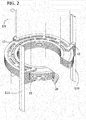
- FIG. 2 is an enlarged fragmentary perspective of the wafer boat and platforms
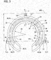
- FIG. 3 is a top view of one of the wafer platforms
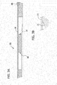
- FIG. 3A is a fragmentary section taken in the plane including line 3A--3A of FIG. 3 and showing a wafer on the platform;
- FIG. 3B is a an enlarged portion of FIG. 3A ;
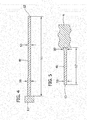
- FIG. 4 is a fragmentary section taken in the plane inducing line 4--4 of FIG. 3 showing a single finger but with the platform removed;
- FIG. 5 is a fragmentary section taken in the plane including line 5--5 of FIG. 3 showing a single finger with the platform removed;
- FIG. 6 is a bottom plan view of one wafer holder platform
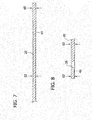
- FIG. 7 is a fragmentary section taken in the plane including line 4--4 of FIG. 3 showing the platform with the finger removed;
- FIG. 8 is a fragmentary section taken in the plane including line 5--5 of FIG. 3 showing the platform with the finger removed;
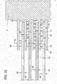
- FIG. 9 is a fragmentary section similar to FIG. 5 , but showing multiple fingers and platforms;
- FIG. 10 is a fragmentary section simitar to FIG. 4 , but showing multiple fingers and platforms;
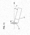
- FIG. 11 is an enlarged plan view of an isolated finger extending from the left forward rod showing the angle at which the finger extends from the rod;
- FIG. 12 is a horizontal cross-section of the wafer boat with another embodiment of the forward rods having wedge-shaped cross-sections.
- FIG. 1 illustrates a semiconductor wafer boat, indicated generally at 1, constructed according to the principles of the present invention.
- the wafer boat 1 includes spaced-apart support rods 3 that are affixed to a top 5 and a base 7 of the boat to retain the positions of the rods relative to each other.
- the support rods 3 are generally vertical.
- the wafer boat 1 has a central rod 9 and two forward rods 11.
- the support rods 3 support laterally extending fingers 13.
- the fingers 13 may be integrally formed on the support rods 3. For example, cuts may be made in an elongate one-piece structure, forming the fingers 13.
- the fingers 13 of the wafer boat 1 are arranged in groups lying in different common generally horizontal planes along the vertical extent of the support rods 3.
- each set of fingers 13 lie in a same generally horizontal plane engage and support a wafer holder platform 20 (broadly, a plate).
- the platform may also be commonly referred to as a support ring.
- the illustrated wafer holder platforms 20 are of an open-ring type generally having a C shape when viewed from above (plan view).
- the open-ring type platform has top and bottom surfaces designated 22 and 24 ( FIG. 6 ), respectively, an outer radius R1, and a hole 28 generally in the center portion of the disk having a radial opening extending from the hole to the outer periphery of the platform 20.
- Other types of wafer platforms including a closed-ring type and a solid plate, are within the scope of this invention.
- the radius R1 is about 150 mm
- a radius R2 of the hole 28 is about 95 mm.
- each wafer bolder platform 20 has a recessed surface 30 defined by an arcuate groove 31 formed In the top surface 22.
- the groove is suitably between about 0.2 mm, and about 0.5 mm deep.
- a pair of spaced apart plateaus 33 (broadly, support surfaces) are disposed on opposite sides of the groove.
- the plateau 33 directly support a semiconductor wafer W ( FIGS. 3A-3B ) white the wafer rests on the wafer holder platform 20. By resting on the plateaus 33 and over the groove 31, the wafer can be removed from the wafer holder platform without the wafer sticking to the wafer holder platform, as is well known in the art.
- each plateau has no holes therein or therethrough.
- each plateau is a substantially smooth, planar surface, without any deviations such as holes, ridges or other features formed therein. Edges of holes or other features, if they existed on the plateaus, could cause contamination of the wafer due to the machining or forming step used to form the holes. Conventional ceramic forming or machining methods used to form the holes introduce the potential of contamination in and around the holes. Also, there is a risk that the edges of holes, if there were any formed in the plateaus, may be sharp and may damage the wafer. Because the plateaus (support surfaces) in this embodiment are free of holes, the wafer W will not be contaminated or damaged by the platform 20. Also, the plateaus 33 on each platform 20 are coplanar so that the wafer W lies flat across the plateaus. Again, the wafer W is not in contact with the recessed surface 30.
- Slots 35 are formed in the recessed surface 30 of one embodiment.
- the slots are suitably formed using conventional ceramic forming tools.
- the slots extend from the recessed surface 30 to the bottom surface 24 ( Fig. 6 ).
- Each slot has an elongate section 36 having an arc or curved shape that generally corresponds to the curve of the groove 31 and to the curve of the outer and inner edges of the platform 20.
- Each slot also has curved ends 37.
- the width of the slot 35 is less the width of the groove 31.
- the slots reduce the area of the platform under the water W to less than 50% in one embodiment, to less than 45% in another embodiment, and to less than 40% in another embodiment.
- the platform of U.S. Pat. No. 7,033,168 has an area under the wafer W of 52% or more.
- the slots do not add significantly to the manufacturing costs of the platform. Further, the slots do not negatively affect the structure of the platform 20.
- the reduction in area is directly proportional to a reduction in thermal mass and to a reduction in the thermal gradient from the center of the wafer W to the edge of the wafer. These reductions also reduce the risk that slip will be created in the wafer W during high temperature processing such as annealing.
- the wafer boat 1 may be made of one of quartz, silicon, silicon nitride, or silicon carbide, or alternatively of a combination of one or more of quartz, silicon, silicon nitride or silicon carbide.
- each finger 13 of the wafer boat 1 has a support location 40 that engages and supports one of the wafer holder platforms 20 ( FIGS, 4 and 5 ).
- each wafer holder platform 20 has tree support locations 43 that engage and are supported by the group of fingers 13 lying in the common horizontal plane ( FIGS. 6 and 10 ).
- Each support location 40 of the finders 13 is adapted to underlie the wafer holder platform 20 at the respective support location 43 of the wafer platform ( FIGS. 7 and 8 ).
- each support location 43 of the wafer holder platforms 20 is adapted to overlie the respective support location 40 of the respective finger 13.
- each finger 13 has a non-uniform thickness along its length L, such that each finger has a first overall maximum thickness 50 which is greater than a second maximum thickness 53.
- the first overall maximum thickness 50 is the thickest part of the entire finger 13, In one embodiment, the first overall maximum thickness 50 is at least about 2.0 mm, and in the illustrated embodiment is about 2.5 mm.
- the second maximum thickness 53 of the finger is the maximum thickness of the finger 13 within the boundaries of the support location 40. In the illustrated embodiment, the support location 40 and the second overall maximum thickness 53 of the finger 13 are located at the free end of the finger.
- the second maximum thickness 53 of the fingers 13 is at least about 0.5 mm, and in the illustrated embodiment is about 2.0 mm.
- the illustrated dimensions of the wafer boat 1 and its components are suitable dimensions for constructing a wafer boat for use in high-temperature heat treatment of 300 mm diameter silicon wafers in a vertical furnace. Other dimensions may be used within the scope of the present invention.
- each wafer holder platform 20 (like each finger 13) has a non-uniform thickness such that each platform has a first overall maximum thickness 60 that is the largest thickness dimension of the entire wafer holder platform.
- the first overall maximum thickness 60 may be at least about 2.0 mm, and in the illustrated embodiment is about 2.0 mm.
- the wafer holder platform 20 has a second maximum thickness 63 at each support location 43 that is less than the first maximum thickness 60 of the wafer holder platform.
- the wafer holder platform 20 has grooves 45 in its bottom surface 24 that correspond to the support locations 43 of the wafer holder platform ( FIG. 6 ).
- the second maximum thickness is at least about 0.5 mm, and in the illustrated embodiment is about 1.0 mm.
- the combined maximum thickness 70 at each support location 40, 43 of the fingers and the platforms that is less than the first overall maximum thickness 50 of each finger plus the first overall maximum thickness 53 of each wafer holder platform.
- the combined maximum thickness at each support location 40, 43 is about 4.0 mm.
- the combined maximum thickness 70 at each support location 40, 43 leaves a vertical space 80 between the platform 20 and the fingers 13 just above the platform.
- the vertical space 80 allows a robotic arm to introduce and remove the wafer. In the illustrated embodiment, the vertical space 80 is about 3.8 mm.
- the illustrated embodiment shows both the fingers 13 and wafer holder platforms 20 having second maximum thicknesses 53, 63 less than the respective first overall maximum thicknesses 50, 60. It is understood, however, that the fingers 13 may not have a second maximum thickness less than the first overall maximum thickness 50. That is, the thickness of each finger 13 may be substantially uniform along its length, and only the wafer holder platforms 20 have a second maximum thickness 63 which is less than the first maximum thickness 60. Alternatively, the wafer holder platforms 20 may not have a second maximum thickness less than the first overall maximum thickness 60. That is, the thickness of each wafer holder platform 20 may be substantially uniform along its length, and only the fingers 13 have a second maximum thickness 53 which is less than the first maximum thickness 50.
- each finger 13 and the thickness of each wafer holder platform 20 at the respective support locations 40,43 By reducing the thickness of each finger 13 and the thickness of each wafer holder platform 20 at the respective support locations 40,43, as described above, the vertical space in the wafer boat 1 occupied by the combined thickness 70 of the each finger and each platform is reduced. This reduction in combined thickness 70 creates more open vertical space within the wafer boat 1, which in turn, can be used to add more fingers 13 and platforms 20. Increasing the number of platforms 20 increases the number of wafers that can be housed in the same vertical space within the water boat 1. Decreasing the vertical space occupied by the combined thickness 70 of each finger 13 and each wafer holder platform 20 at the respective support locations 40, 43 increases wafer throughput of the vertical furnace and production of heat-treated semiconductor wafers, while decreasing production costs. However, the combined thickness of each finger 13 and each wafer holder platform 20 at the respective support locations 40, 43 is sufficient to provide a stable foundation for holding the wafer so as to avoid slip and plastic deformation of the wafer during
- the illustrated wafer boat 1 of the present invention can hold up to about 135 wafers or about 1.2 wafers per centimeter of height of the wafer boat.
- the overall height of the wafer boat 1 of the illustrated embodiment is such that it can fit within a quartz tube of an ASM® A412 vertical furnace.
- a wafer boat 1 constructed according to the teachings of the prior art typically holds less than 1 wafer per centimeter of height of the wafer boat.
- the wafer boat 1 of the present invention increases throughput by up to 50% without, as stated above, compromising wafer quality.
- points nearest to the central rod 9 where the forward rod fingers 13 and the forward rods 11 meet are designated 90. These points 90 are located in a forward vertical plane VP1 that is spaced forward from a parallel rear vertical plane VP2 that is tangent to the wafer boat 1 at the back of the boat. In the illustrated embodiment, the central rod 9 defines the back of the wafer boat 1.
- the optimal configuration of the support rods 3 and fingers 13 i.e., the arrangement of the rods and fingers that would give the most support to the wafer holder platforms is where the rods are spaced equidistantly apart forming an equilateral triangle arrangement and the fingers extend toward the center of the wafer holder platform 20.
- the support of the fingers 13 is equally distributed along the circumference of the wafer holder platform 20.
- this optimal configuration is not feasible for use with 300 mm and larger diameter wafer boats because of dimensional constraints imposed by the diameter of the wafers to be received in the boat and the internal diameter of the vertical furnace.
- the distance between two support rods 3 must be greater than the diameter of the wafer, e.g., 300 mm, so that the wafer can be received within the boat (e.g., between the forward rods 11).
- the cross-sectional diameter of the wafer boat 1 cannot be greater than the internal diameter of a quartz tube of the vertical furnace, or else the boat will not fit in the furnace.
- the internal diameter of a quartz tube for the ASM A412 vertical furnace is about 340 mm.
- Positioning the three support rods 3 at least 300 mm apart (since they are optimally in an equilateral triangle arrangement) makes the diameter of the wafer boat 1 much greater than the internal diameter of the quartz tube, and the boat would not fit in the furnace. It is noted that even if a larger diameter furnace were possible, an equilateral triangle arrangement of the support rods 3 would require very long fingers 13, resulting in a wafer boat with low mechanical stability because of the lengths of the fingers.
- the prior art teaches the configuration of the forward rods 11 spaced apart the minimal distance necessary to allow the wafers to be received in the boat 1 (e.g., in the illustrated embodiment the distance is based on 300 mm wafers) and positioned in the forward vertical plane VP1 as far away from the rear vertical plane VP2 as possible without wafer boat exceeding its diameter constraint imposed by the internal diameter of the vertical furnace.
- the fingers 13 extending from the forward rods 11 also lie in the forward plane VP1. This configuration is an attempt to best distribute the support of the fingers 13 along the circumference of the wafer holder platform 20 while staying within the imposed constraints.
- this configuration may not adequately support the area of the wafer holder platform 20 forward of the forward plane VP1. Inadequate support of the wafer holder platform 20 forward of the forward rods 11 may cause plastic deformation of the wafer platform 20 (especially in the open ring type of the illustrated embodiment) leading to slip and possibly plastic deformation in the silicon wafers during high-temperature heat treatment in the vertical furnace.
- the fingers 13 on the forward rods 11 are angled forward an angle A relative to the forward plane VP1 to allow the support locations 40 of the fingers to underlie portions of the areas of the wafer holder platforms 20 that are forward of the forward plane VP1 ( FIG. 12 ).
- the angle A is between 10 and 20 degrees, and in the illustrated embodiment is about 15 degrees.
- the fingers 13 on the forward rods 11 must typically be longer than the fingers on the central rod 9 because the forward rod fingers must extend to a more forward location nearer to the ideal, equilateral location for supporting the wafer holder platform 20.
- a length L1 of each finger 13 of the forward rods 11 is about 60 mm ( FIG. 4 ).
- a length L2 of each finger 13 of the central rod 9 is about 28 mm ( FIG. 5 ).
- Other lengths consistent with the teachings of the present invention are contemplated.
- increasing the lengths L1, L2 of the fingers 13 decreases their mechanical stability. This decrease in mechanical stability could lead to plastic deformation and inadequate support or even failure.
- the fingers 13 of the forward rods 11 have the lengths L1 so that they extend as far forward as possible without exceeding dimensional constraints for mechanical stability.
- the wafer boat 1 is by placing the wafer holder platforms 20 on the respective fingers 13. Wafers are loaded into the boat 1 so that each wafer is placed on the top surface 22 of one wafer holder platform 20. Typically, the wafers are loaded via a robotic arm, as is well known in the art. Once the boat 1 is loaded with a predetermined number of wafers (ranging from 1 wafer to about 135 wafers using the illustrated embodiment), the boat is received in the vertical furnace. The high-temperature heat treatment is performed, as is well known in the art. Space is provided between each wafer and the wafer holder platform 20 to receive a portion of the robotic arm. After heat treatment and other treatment, the wafers are unloaded from the boat 1, typically using the robotic arm.
- the cross-sections of side support rods 100 are wedge-shaped.
- the side rods 100 each have a tapered cross-section where the cross-section of the rod tapers in the direction of the fingers 13.
- the outer surfaces 105 of the side rods curve toward the finger such that substantially the entireties of the outer surfaces lie on the circumference of the cross-section of the wafer boat 1.
- a forward vertical plane VP3 is defined by points 110 nearest to the central rod 9 (i.e., most rear points) where the forward rod fingers 13 and the forward rods 100 meet. This forward vertical plane VP3 is spaced apart a distance D2 from the rear vertical plane VP2.
- the forward vertical plane VP3 (i.e., the wedge-shaped rods 100) may be located even more forward from the rear vertical plane VP2 than the diamond-shaped rods 11 while staying within the internal diameter constraints of the quartz tube of the vertical furnace.
- the distance D2 between the forward and rear planes VP3, VP2 is about 227 mm, or about 76% of the nominal diameter of the wafer.
Landscapes
- Container, Conveyance, Adherence, Positioning, Of Wafer (AREA)
Abstract
A support for a semiconductor wafer includes a plate having a support surface for supporting the wafer and a recessed surface spaced from the support surface and spaced from the wafer. A plurality of holes extends from the recessed surface, and the support surface is free of holes to inhibit contamination of the wafer.
Description
- This invention relates generally to semiconductor wafer supports, and more particularly to a low thermal mass semiconductor wafer support for use in heat treatment of semiconductor wafers in a furnace.
- High temperature heat-treatment (e.g., annealing) of semiconductor wafers is commonly used to achieve certain desirable characteristics. For example, such a process may be used to create a defect free layer of silicon on the wafers. The high temperature annealing process of the type to which the present invention particularly relates is carried out in a vertical furnace which typically subjects the wafers to temperature above 1100 degrees C, e.g., between about 1200 degrees C and about 1300 degrees C.
- During high temperature heat-treatment, at temperatures above 750 degrees C and especially above 1100 degrees C, the silicon wafers become more plastic. If the silicon wafers are not adequately supported, during heat treatment, the wafers may undergo slip due to local gravitational, and thermal stresses. As is well known in the art, slip may introduce contaminants into the device areas of the wafers. Moreover, excessive slip may lead to plastic deformation of the wafers, which in turn may lead to production problems, such as photolithography overlay failures causing yield losses in device manufacture.
- Vertical wafer boats or racks are used to adequately support semiconductor wafers, and, to minimize the local gravitational and thermal stresses. The support attempts to prevent slip and plastic deformation while the wafers are being heat treated. A typical vertical wafer boat used in a vertical furnace comprises three or more vertical rails also referred to as rods, The rods typically have grooves or laterally extending fingers for supporting the wafers between the vertical rods within the boat. Each wafer may rest directly on fingers (or grooves) lying generally in a common horizontal plane. This configuration is common in the older art and is adequate when heat treating 200 mm and smaller diameter wafers. Alternatively, each wafer may rest on a wafer holder platform, e.g., a ring or solid plate, supported by the fingers (or in grooves), lying generally in a common horizontal plane. This configuration is common in the newer art and is usually necessary to adequately support 300 mm and larger diameter wafers. The 300 mm and larger diameter wafers are subjected to more local gravitational and thermal stresses than smaller diameter wafers, and the wafer holder platforms better support the 300 mm wafers by increasing the areas of the wafers that are supported.
- Co-assigned
U.S. Pat. No. 7,033,168 , which is incorporated herein by reference, shows one suitable type of wafer boat for use in the above-described process.WO 2006/118774 ('774) shows another type that includes shelves for supporting the wafers. Eachshelf 24 includes a plurality of holes 32, 34 that "are useful to relieve stress in thethin shelves 24, to reduce thermal mass, and to allow the furnace ambient to reach a substantial portion of the wafer backside, thereby preventing the wafers from sticking to theshelves 24. The planar shape of theshelf 24 allows it to be economically machined from slices of material, especially silicon, similar to wafers." - However, there are certain shortcomings in the prior art supports. For example, placing the wafers in contact with the hole edges of the '774 shelf will cause contamination of the wafer. Additionally, the '774 configuration will cause slip in the wafer. A better wafer support that will not cause contamination or slip is needed.
- In one aspect, a support for a semiconductor wafer includes a plate having a support surface for supporting the wafer and a recessed surface spaced from the support surface and spaced from the wafer. A plurality of holes extends from the recessed surface, and the support surface is free of holes to inhibit contamination of the wafer.
- In another aspect, a plate for supporting the semiconductor wafer includes top and bottom surfaces. The top surface includes a support surface and a recessed surface spaced vertically from the support surface. The plate includes a plurality of holes that extend from the recessed surface to the bottom surface. The support surface is free of holes.
- In still another aspect, a wafer boat is for use in heat treatment of semiconductor wafers in a furnace. The boat includes vertical rods, fingers supported by the vertical rods and plates supported by the fingers. At least some of the plates include a support surface for supporting the wafer and a recessed surface spaced from the support surface and spaced from the wafer. A plurality of holes extends from the recessed surface, and the support surface is free of holes to inhibit contamination of the wafer.
- Various refinements exist of the features noted in relation to the above-mentioned aspects. Further features may also be incorporated in the above-mentioned aspects as well. These refinements and additional features may exist individually or in any combination. For instance, various features discussed below in relation to any of the illustrated embodiments may be incorporated into any of the above-described aspects, alone or in any combination.
-
FIG. 1 is a perspective of a wafer boat having wafer holder platforms of one embodiment; -
FIG. 2 is an enlarged fragmentary perspective of the wafer boat and platforms; -
FIG. 3 is a top view of one of the wafer platforms; -
FIG. 3A is a fragmentary section taken in theplane including line 3A--3A ofFIG. 3 and showing a wafer on the platform; -
FIG. 3B is a an enlarged portion ofFIG. 3A ; -
FIG. 4 is a fragmentary section taken in theplane inducing line 4--4 ofFIG. 3 showing a single finger but with the platform removed; -
FIG. 5 is a fragmentary section taken in theplane including line 5--5 ofFIG. 3 showing a single finger with the platform removed; -
FIG. 6 is a bottom plan view of one wafer holder platform; -
FIG. 7 is a fragmentary section taken in theplane including line 4--4 ofFIG. 3 showing the platform with the finger removed; -
FIG. 8 is a fragmentary section taken in theplane including line 5--5 ofFIG. 3 showing the platform with the finger removed; -
FIG. 9 is a fragmentary section similar toFIG. 5 , but showing multiple fingers and platforms; -
FIG. 10 is a fragmentary section simitar toFIG. 4 , but showing multiple fingers and platforms; -
FIG. 11 is an enlarged plan view of an isolated finger extending from the left forward rod showing the angle at which the finger extends from the rod; and -
FIG. 12 is a horizontal cross-section of the wafer boat with another embodiment of the forward rods having wedge-shaped cross-sections. - Corresponding reference characters indicate corresponding throughout the drawings. Corresponding reference characters indicate corresponding parts throughout the drawings.
- Referring now to the drawings and in particular to
FIG. 1 which illustrates a semiconductor wafer boat, indicated generally at 1, constructed according to the principles of the present invention. Thewafer boat 1 includes spaced-apart support rods 3 that are affixed to atop 5 and abase 7 of the boat to retain the positions of the rods relative to each other. When thewafer boat 1 is placed in a vertical furnace, the support rods 3 are generally vertical. In the illustrated embodiment, thewafer boat 1 has acentral rod 9 and twoforward rods 11. - The support rods 3 support laterally extending
fingers 13. Thefingers 13 may be integrally formed on the support rods 3. For example, cuts may be made in an elongate one-piece structure, forming thefingers 13. Thefingers 13 of thewafer boat 1 are arranged in groups lying in different common generally horizontal planes along the vertical extent of the support rods 3. - Referring to
FIGS. 2-3 , each set offingers 13 lie in a same generally horizontal plane engage and support a wafer holder platform 20 (broadly, a plate). The platform may also be commonly referred to as a support ring. The illustratedwafer holder platforms 20 are of an open-ring type generally having a C shape when viewed from above (plan view). - The open-ring type platform has top and bottom surfaces designated 22 and 24 (
FIG. 6 ), respectively, an outer radius R1, and ahole 28 generally in the center portion of the disk having a radial opening extending from the hole to the outer periphery of theplatform 20. Other types of wafer platforms, including a closed-ring type and a solid plate, are within the scope of this invention. For a wafer platform used to support 300 wafers, the radius R1 is about 150 mm, and a radius R2 of thehole 28 is about 95 mm. - In the illustrated embodiment, each wafer
bolder platform 20 has a recessed surface 30 defined by anarcuate groove 31 formed In thetop surface 22. The groove is suitably between about 0.2 mm, and about 0.5 mm deep. A pair of spaced apart plateaus 33 (broadly, support surfaces) are disposed on opposite sides of the groove. Theplateau 33 directly support a semiconductor wafer W (FIGS. 3A-3B ) white the wafer rests on thewafer holder platform 20. By resting on theplateaus 33 and over thegroove 31, the wafer can be removed from the wafer holder platform without the wafer sticking to the wafer holder platform, as is well known in the art. - Additionally, the
plateaus 33 have no holes therein or therethrough. In other words, each plateau is a substantially smooth, planar surface, without any deviations such as holes, ridges or other features formed therein. Edges of holes or other features, if they existed on the plateaus, could cause contamination of the wafer due to the machining or forming step used to form the holes. Conventional ceramic forming or machining methods used to form the holes introduce the potential of contamination in and around the holes. Also, there is a risk that the edges of holes, if there were any formed in the plateaus, may be sharp and may damage the wafer. Because the plateaus (support surfaces) in this embodiment are free of holes, the wafer W will not be contaminated or damaged by theplatform 20. Also, theplateaus 33 on eachplatform 20 are coplanar so that the wafer W lies flat across the plateaus. Again, the wafer W is not in contact with the recessed surface 30. - Slots 35 (broadly, holes) are formed in the recessed surface 30 of one embodiment. The slots are suitably formed using conventional ceramic forming tools. The slots extend from the recessed surface 30 to the bottom surface 24 (
Fig. 6 ). Each slot has anelongate section 36 having an arc or curved shape that generally corresponds to the curve of thegroove 31 and to the curve of the outer and inner edges of theplatform 20. Each slot also has curved ends 37. The width of theslot 35 is less the width of thegroove 31. - The slots reduce the area of the platform under the water W to less than 50% in one embodiment, to less than 45% in another embodiment, and to less than 40% in another embodiment. Note that the platform of
U.S. Pat. No. 7,033,168 has an area under the wafer W of 52% or more. The slots do not add significantly to the manufacturing costs of the platform. Further, the slots do not negatively affect the structure of theplatform 20. The reduction in area is directly proportional to a reduction in thermal mass and to a reduction in the thermal gradient from the center of the wafer W to the edge of the wafer. These reductions also reduce the risk that slip will be created in the wafer W during high temperature processing such as annealing. - It will be understood that constructions (not shown) other than those just described can be used within the scope of the present invention. The
wafer boat 1 may be made of one of quartz, silicon, silicon nitride, or silicon carbide, or alternatively of a combination of one or more of quartz, silicon, silicon nitride or silicon carbide. - Referring now to
FIGS. 4-10 , eachfinger 13 of thewafer boat 1 has asupport location 40 that engages and supports one of the wafer holder platforms 20 (FIGS, 4 and 5 ). Similarly, eachwafer holder platform 20 hastree support locations 43 that engage and are supported by the group offingers 13 lying in the common horizontal plane (FIGS. 6 and10 ). Eachsupport location 40 of thefinders 13 is adapted to underlie thewafer holder platform 20 at therespective support location 43 of the wafer platform (FIGS. 7 and 8 ). Similarly, eachsupport location 43 of thewafer holder platforms 20 is adapted to overlie therespective support location 40 of therespective finger 13. - Referring particularly to
FIGS. 4 and 5 , eachfinger 13 has a non-uniform thickness along its length L, such that each finger has a first overallmaximum thickness 50 which is greater than a secondmaximum thickness 53. The first overallmaximum thickness 50 is the thickest part of theentire finger 13, In one embodiment, the first overallmaximum thickness 50 is at least about 2.0 mm, and in the illustrated embodiment is about 2.5 mm. The secondmaximum thickness 53 of the finger is the maximum thickness of thefinger 13 within the boundaries of thesupport location 40. In the illustrated embodiment, thesupport location 40 and the second overallmaximum thickness 53 of thefinger 13 are located at the free end of the finger. The secondmaximum thickness 53 of thefingers 13 is at least about 0.5 mm, and in the illustrated embodiment is about 2.0 mm. The illustrated dimensions of thewafer boat 1 and its components (given above and hereinafter) are suitable dimensions for constructing a wafer boat for use in high-temperature heat treatment of 300 mm diameter silicon wafers in a vertical furnace. Other dimensions may be used within the scope of the present invention. - Referring particularly to
FIGS. 7 and 8 , each wafer holder platform 20 (like each finger 13) has a non-uniform thickness such that each platform has a first overallmaximum thickness 60 that is the largest thickness dimension of the entire wafer holder platform. The first overallmaximum thickness 60 may be at least about 2.0 mm, and in the illustrated embodiment is about 2.0 mm. Thewafer holder platform 20 has a secondmaximum thickness 63 at eachsupport location 43 that is less than the firstmaximum thickness 60 of the wafer holder platform. In the illustrated embodiment, thewafer holder platform 20 has grooves 45 in itsbottom surface 24 that correspond to thesupport locations 43 of the wafer holder platform (FIG. 6 ). The second maximum thickness is at least about 0.5 mm, and in the illustrated embodiment is about 1.0 mm. - Referring particularly to
FIGS. 9 and10 , when thewafer holder platforms 20 are resting on thefingers 13, there is a combinedmaximum thickness 70 at eachsupport location maximum thickness 50 of each finger plus the first overallmaximum thickness 53 of each wafer holder platform. In the illustrated embodiment, the combined maximum thickness at eachsupport location maximum thickness 70 at eachsupport location vertical space 80 between theplatform 20 and thefingers 13 just above the platform. Thevertical space 80 allows a robotic arm to introduce and remove the wafer. In the illustrated embodiment, thevertical space 80 is about 3.8 mm. - As described above, the illustrated embodiment shows both the
fingers 13 andwafer holder platforms 20 having secondmaximum thicknesses maximum thicknesses fingers 13 may not have a second maximum thickness less than the first overallmaximum thickness 50. That is, the thickness of eachfinger 13 may be substantially uniform along its length, and only thewafer holder platforms 20 have a secondmaximum thickness 63 which is less than the firstmaximum thickness 60. Alternatively, thewafer holder platforms 20 may not have a second maximum thickness less than the first overallmaximum thickness 60. That is, the thickness of eachwafer holder platform 20 may be substantially uniform along its length, and only thefingers 13 have a secondmaximum thickness 53 which is less than the firstmaximum thickness 50. It is noted that these embodiments are satisfactory for the intended purpose of the present invention as long as the combinedmaximum thickness 70 at eachsupport location finders 13 andwafer holder platforms 20 is less than the combined firstmaximum thicknesses fingers 13 andwafer holder platforms 20. - By reducing the thickness of each
finger 13 and the thickness of eachwafer holder platform 20 at therespective support locations wafer boat 1 occupied by the combinedthickness 70 of the each finger and each platform is reduced. This reduction in combinedthickness 70 creates more open vertical space within thewafer boat 1, which in turn, can be used to addmore fingers 13 andplatforms 20. Increasing the number ofplatforms 20 increases the number of wafers that can be housed in the same vertical space within thewater boat 1. Decreasing the vertical space occupied by the combinedthickness 70 of eachfinger 13 and eachwafer holder platform 20 at therespective support locations finger 13 and eachwafer holder platform 20 at therespective support locations - The illustrated
wafer boat 1 of the present invention can hold up to about 135 wafers or about 1.2 wafers per centimeter of height of the wafer boat. The overall height of thewafer boat 1 of the illustrated embodiment is such that it can fit within a quartz tube of an ASM® A412 vertical furnace. Awafer boat 1 constructed according to the teachings of the prior art typically holds less than 1 wafer per centimeter of height of the wafer boat. Thus, thewafer boat 1 of the present invention increases throughput by up to 50% without, as stated above, compromising wafer quality. - Referring to
FIG. 3 , points nearest to the central rod 9 (i.e., most rear points) where theforward rod fingers 13 and theforward rods 11 meet are designated 90. Thesepoints 90 are located in a forward vertical plane VP1 that is spaced forward from a parallel rear vertical plane VP2 that is tangent to thewafer boat 1 at the back of the boat. In the illustrated embodiment, thecentral rod 9 defines the back of thewafer boat 1. The optimal configuration of the support rods 3 and fingers 13 (i.e., the arrangement of the rods and fingers that would give the most support to the wafer holder platforms) is where the rods are spaced equidistantly apart forming an equilateral triangle arrangement and the fingers extend toward the center of thewafer holder platform 20. In this arrangement, the support of thefingers 13 is equally distributed along the circumference of thewafer holder platform 20. However, this optimal configuration is not feasible for use with 300 mm and larger diameter wafer boats because of dimensional constraints imposed by the diameter of the wafers to be received in the boat and the internal diameter of the vertical furnace. The distance between two support rods 3 must be greater than the diameter of the wafer, e.g., 300 mm, so that the wafer can be received within the boat (e.g., between the forward rods 11). Moreover, the cross-sectional diameter of thewafer boat 1 cannot be greater than the internal diameter of a quartz tube of the vertical furnace, or else the boat will not fit in the furnace. For example, the internal diameter of a quartz tube for the ASM A412 vertical furnace is about 340 mm. Positioning the three support rods 3 at least 300 mm apart (since they are optimally in an equilateral triangle arrangement) makes the diameter of thewafer boat 1 much greater than the internal diameter of the quartz tube, and the boat would not fit in the furnace. It is noted that even if a larger diameter furnace were possible, an equilateral triangle arrangement of the support rods 3 would require verylong fingers 13, resulting in a wafer boat with low mechanical stability because of the lengths of the fingers. - Because the support rods 3 cannot be equidistantly spaced apart, the prior art teaches the configuration of the
forward rods 11 spaced apart the minimal distance necessary to allow the wafers to be received in the boat 1 (e.g., in the illustrated embodiment the distance is based on 300 mm wafers) and positioned in the forward vertical plane VP1 as far away from the rear vertical plane VP2 as possible without wafer boat exceeding its diameter constraint imposed by the internal diameter of the vertical furnace. Thefingers 13 extending from theforward rods 11 also lie in the forward plane VP1. This configuration is an attempt to best distribute the support of thefingers 13 along the circumference of thewafer holder platform 20 while staying within the imposed constraints. However, this configuration may not adequately support the area of thewafer holder platform 20 forward of the forward plane VP1. Inadequate support of thewafer holder platform 20 forward of theforward rods 11 may cause plastic deformation of the wafer platform 20 (especially in the open ring type of the illustrated embodiment) leading to slip and possibly plastic deformation in the silicon wafers during high-temperature heat treatment in the vertical furnace. - In one embodiment of the
wafer boat 1 of the present invention, thefingers 13 on theforward rods 11 are angled forward an angle A relative to the forward plane VP1 to allow thesupport locations 40 of the fingers to underlie portions of the areas of thewafer holder platforms 20 that are forward of the forward plane VP1 (FIG. 12 ). The angling of thefingers 13 on theforward rods 11, in effect, gives greater support to the forward part of thewafer holder platform 20 than would be given if the fingers extended along the forward plane VP1 (as in the prior art). In one embodiment, the angle A is between 10 and 20 degrees, and in the illustrated embodiment is about 15 degrees. - The
fingers 13 on theforward rods 11 must typically be longer than the fingers on thecentral rod 9 because the forward rod fingers must extend to a more forward location nearer to the ideal, equilateral location for supporting thewafer holder platform 20. In the illustrated embodiment, a length L1 of eachfinger 13 of theforward rods 11 is about 60 mm (FIG. 4 ). Also in the illustrated embodiment, a length L2 of eachfinger 13 of thecentral rod 9 is about 28 mm (FIG. 5 ). Other lengths consistent with the teachings of the present invention are contemplated. As is well known in the art, during high-temperature heat treatment, increasing the lengths L1, L2 of thefingers 13 decreases their mechanical stability. This decrease in mechanical stability could lead to plastic deformation and inadequate support or even failure. Thefingers 13 of theforward rods 11 have the lengths L1 so that they extend as far forward as possible without exceeding dimensional constraints for mechanical stability. - In use, the
wafer boat 1 is by placing thewafer holder platforms 20 on therespective fingers 13. Wafers are loaded into theboat 1 so that each wafer is placed on thetop surface 22 of onewafer holder platform 20. Typically, the wafers are loaded via a robotic arm, as is well known in the art. Once theboat 1 is loaded with a predetermined number of wafers (ranging from 1 wafer to about 135 wafers using the illustrated embodiment), the boat is received in the vertical furnace. The high-temperature heat treatment is performed, as is well known in the art. Space is provided between each wafer and thewafer holder platform 20 to receive a portion of the robotic arm. After heat treatment and other treatment, the wafers are unloaded from theboat 1, typically using the robotic arm. - In another embodiment of the present invention, illustrated in
FIG. 12 , the cross-sections ofside support rods 100 are wedge-shaped. Theside rods 100 each have a tapered cross-section where the cross-section of the rod tapers in the direction of thefingers 13. Theouter surfaces 105 of the side rods curve toward the finger such that substantially the entireties of the outer surfaces lie on the circumference of the cross-section of thewafer boat 1. A forward vertical plane VP3 is defined bypoints 110 nearest to the central rod 9 (i.e., most rear points) where theforward rod fingers 13 and theforward rods 100 meet. This forward vertical plane VP3 is spaced apart a distance D2 from the rear vertical plane VP2. The forward vertical plane VP3 (i.e., the wedge-shaped rods 100) may be located even more forward from the rear vertical plane VP2 than the diamond-shapedrods 11 while staying within the internal diameter constraints of the quartz tube of the vertical furnace. In the illustrated embodiment, the distance D2 between the forward and rear planes VP3, VP2 is about 227 mm, or about 76% of the nominal diameter of the wafer. - When introducing elements of the present invention or the embodiment(s) thereof, the articles "a", "an", "the" and "said" are intended to mean that there are one or more of the elements. The terms "comprising", "including" and "having" are intended to be inclusive and mean that there may be additional elements other than the listed elements.
- As various changes could be made in the above constructions without departing from the scope of the invention, it is intended that all mater contained in the above description and shown in the accompanying drawing[s] shall be interpreted as illustrative and not in a limiting sense.
-
- 1. A support for a semiconductor wafer comprising a plate including a support surface for supporting the wafer and a recessed surface spaced from the support surface and thereby spaced from the wafer, a plurality of holes extending from the recessed surface, and the support surface being free of holes to inhibit contamination of the wafer.
- 2. The support of
item 1 in combination with a wafer boat. - 3. The support of
items 1 or 2 in combination with a semiconductor water. - 4. The support of any of items 1-3 wherein the plate is C shaped.
- 5. The support of any of items 1-4 wherein the holes are arc-shaped.
- 6. The support of any of items 1-5 wherein the plate has a bottom surface and the holes extend from the recessed surface through to the bottom surface.
- 7. The support of any of items 1-6 wherein the area of the plate is less than 50% of that of the wafer.
- 8. The support of any of items 1-7 wherein the area of the plate is less than 40% of that of the wafer.
- 9. The support of any of items 1-8 wherein the plate is made of one of silicon carbide, silicon nitride and silicon.
- 10. A plate for supporting a semiconductor wafer comprising top and bottom surfaces, the top surface including a support surface and a recessed surface spaced vertically from the support surface, the plate including a plurality of holes that extend from the recessed surface to the bottom surface, the support surface being free of holes.
- 11. The support of item 10 wherein the plate is C shaped.
- 12. The support of
item 10 or 11 wherein the holes are arc-shaped. - 13. The support of any of items 10-12 wherein the area of the plate is less than 50% of that of the wafer.
- 14. The support of any of items 10-13 wherein the area of the plate is less than 40% of that of the wafer.
- 15. The support of any of tems 10-14 wherein the plate is made of one of silicon carbide, silicon nitride and silicon.
- 16. A wafer boat for use in heat treatment of semiconductor wafers in a furnace, the boat comprising:
- vertical rods,
- fingers supported by the vertical rods and
- plates supported by the fingers,
- at least some of the plates including a support surface for supporting the wafer and a recessed surface spaced from the support surface and thereby spaced from the wafer, a plurality of holes extending from the recessed surface, and the support surface being free of holes to inhibit contamination of the wafer.
- 17. The support of item 16 in combination with a semiconductor wafer.
- 18. The support of item 16 or 17 wherein at least some of the plates are C shaped and the holes therein are arc-shaped.
- 19. The support of any of items 16-18 wherein each plate has a bottom surface and the holes extend from the recessed surface through to the bottom surface.
- 20. The support of any of items 16-19 wherein the area of each plate is less than 50% of that of the wafer.
Claims (9)
- A plate for supporting a semiconductor wafer, the plate comprising top and bottom surfaces, the top surface including a planar support surface and a recessed surface spaced vertically downward below the support surface, the plate including a plurality of holes that extend from the recessed surface to the bottom surface, the support surface being free of holes, wherein the plurality of holes inhibit slip in the semiconductor wafer during high temperature processing of the semiconductor wafer.
- The plate of claim 1 wherein the holes are arc-shaped.
- The plate of claim 1 or 2 wherein the plate is C-shaped.
- The plate of any one of claims 1 to 3 wherein the area of the plate is less than 50% of that of the wafer.
- The plate of claim 4 wherein the area of the plate is less than 40% of that of the wafer.
- The plate of any one of claims 1 to 5 wherein the plate is made of one of silicon carbide, silicon nitride and silicon.
- The plate of any one of claims 1 to 6 wherein the planar support surface includes two plateaus separated by the recessed surface.
- The plate of claim 7 wherein the recessed surface is defined by a groove.
- The plate of any one of claims 1 to 8 in combination with a semiconductor wafer.
Applications Claiming Priority (2)
| Application Number | Priority Date | Filing Date | Title |
|---|---|---|---|
| US12/165,048 US8042697B2 (en) | 2008-06-30 | 2008-06-30 | Low thermal mass semiconductor wafer support |
| EP09774069A EP2311080B1 (en) | 2008-06-30 | 2009-06-22 | Low thermal mass semiconductor wafer support |
Related Parent Applications (1)
| Application Number | Title | Priority Date | Filing Date |
|---|---|---|---|
| EP09774069.0 Division | 2009-06-22 |
Publications (1)
| Publication Number | Publication Date |
|---|---|
| EP2597672A2 true EP2597672A2 (en) | 2013-05-29 |
Family
ID=40912053
Family Applications (3)
| Application Number | Title | Priority Date | Filing Date |
|---|---|---|---|
| EP09774069A Active EP2311080B1 (en) | 2008-06-30 | 2009-06-22 | Low thermal mass semiconductor wafer support |
| EP13155744.9A Withdrawn EP2597672A2 (en) | 2008-06-30 | 2009-06-22 | Low thermal mass semiconductor wafer plate |
| EP13155747.2A Withdrawn EP2597673A2 (en) | 2008-06-30 | 2009-06-22 | Low thermal mass semiconductor wafer boat |
Family Applications Before (1)
| Application Number | Title | Priority Date | Filing Date |
|---|---|---|---|
| EP09774069A Active EP2311080B1 (en) | 2008-06-30 | 2009-06-22 | Low thermal mass semiconductor wafer support |
Family Applications After (1)
| Application Number | Title | Priority Date | Filing Date |
|---|---|---|---|
| EP13155747.2A Withdrawn EP2597673A2 (en) | 2008-06-30 | 2009-06-22 | Low thermal mass semiconductor wafer boat |
Country Status (7)
| Country | Link |
|---|---|
| US (3) | US8042697B2 (en) |
| EP (3) | EP2311080B1 (en) |
| JP (1) | JP5436552B2 (en) |
| KR (1) | KR20110025781A (en) |
| CN (1) | CN102077336A (en) |
| TW (1) | TWI430391B (en) |
| WO (1) | WO2010002617A1 (en) |
Families Citing this family (20)
| Publication number | Priority date | Publication date | Assignee | Title |
|---|---|---|---|---|
| US20090162183A1 (en) * | 2007-12-19 | 2009-06-25 | Peter Davison | Full-contact ring for a large wafer |
| US8042697B2 (en) * | 2008-06-30 | 2011-10-25 | Memc Electronic Materials, Inc. | Low thermal mass semiconductor wafer support |
| JP5565242B2 (en) * | 2010-09-29 | 2014-08-06 | 東京エレクトロン株式会社 | Vertical heat treatment equipment |
| JP5881956B2 (en) * | 2011-02-28 | 2016-03-09 | 株式会社日立国際電気 | Substrate processing apparatus, semiconductor device manufacturing method, and wafer holder |
| USD763807S1 (en) * | 2014-05-22 | 2016-08-16 | Hzo, Inc. | Boat for a deposition apparatus |
| US9099514B2 (en) | 2012-03-21 | 2015-08-04 | Taiwan Semiconductor Manufacturing Company, Ltd. | Wafer holder with tapered region |
| US10190235B2 (en) * | 2013-05-24 | 2019-01-29 | Taiwan Semiconductor Manufacturing Company, Ltd. | Wafer supporting structure and method for forming the same |
| JP6321172B2 (en) * | 2013-11-25 | 2018-05-09 | アプライド マテリアルズ インコーポレイテッドApplied Materials,Incorporated | Substrate carrier for thermal energy transfer reduction |
| KR20150110207A (en) * | 2014-03-24 | 2015-10-02 | 주식회사 테라세미콘 | Boat |
| US10072892B2 (en) * | 2015-10-26 | 2018-09-11 | Globalwafers Co., Ltd. | Semiconductor wafer support ring for heat treatment |
| DE102015014903A1 (en) * | 2015-11-18 | 2017-05-18 | Centrotherm Photovoltaics Ag | Wafer boat and plasma treatment device for wafers |
| JP6770461B2 (en) * | 2017-02-21 | 2020-10-14 | クアーズテック株式会社 | Vertical wafer boat |
| US20210233783A1 (en) * | 2018-06-25 | 2021-07-29 | LINDENBERG Ralph | Carrier for a substrate and method for carrying a substrate |
| TWI735115B (en) * | 2019-12-24 | 2021-08-01 | 力成科技股份有限公司 | A wafer storage cassette and a wafer carrier plate |
| US12046495B2 (en) * | 2020-06-26 | 2024-07-23 | Globalwafers Co., Ltd. | Wafer boats for supporting semiconductor wafers in a furnace |
| JP7734211B2 (en) * | 2021-05-12 | 2025-09-04 | アプライド マテリアルズ インコーポレイテッド | Low mass substrate support |
| CN113964071A (en) * | 2021-11-25 | 2022-01-21 | 滁州钰顺企业管理咨询合伙企业(有限合伙) | Method for reducing wafer package damage |
| US12261068B2 (en) * | 2022-10-27 | 2025-03-25 | Intel Corporation | Wafer support member and method of manufacturing a wafer support member |
| EP4498411A3 (en) * | 2023-06-28 | 2025-03-26 | ASM IP Holding B.V. | Wafer boat system, holder ring and use thereof |
| TWI911672B (en) * | 2024-03-13 | 2026-01-11 | 力晶積成電子製造股份有限公司 | Wafer holding device |
Citations (2)
| Publication number | Priority date | Publication date | Assignee | Title |
|---|---|---|---|---|
| US7033168B1 (en) | 2005-01-24 | 2006-04-25 | Memc Electronic Materials, Inc. | Semiconductor wafer boat for a vertical furnace |
| WO2006118774A2 (en) | 2005-05-03 | 2006-11-09 | Integrated Materials, Inc. | Silicon shelf towers |
Family Cites Families (42)
| Publication number | Priority date | Publication date | Assignee | Title |
|---|---|---|---|---|
| US1587693A (en) * | 1924-07-26 | 1926-06-08 | Edith M Beland | Attachment for sinks |
| US5199582A (en) * | 1990-05-14 | 1993-04-06 | Halstrick Robert T | Storage rack shelving with improved fire protection |
| JP3125199B2 (en) * | 1993-03-18 | 2001-01-15 | 東京エレクトロン株式会社 | Vertical heat treatment equipment |
| JPH07254591A (en) * | 1994-03-16 | 1995-10-03 | Toshiba Corp | Heat treatment equipment |
| KR0135049B1 (en) * | 1994-05-31 | 1998-04-20 | 양승택 | Wafer cassette for semiconductor fabrication |
| JP3692697B2 (en) | 1997-03-25 | 2005-09-07 | 三菱住友シリコン株式会社 | Wafer support and vertical boat |
| JPH11260746A (en) | 1998-03-13 | 1999-09-24 | Sumitomo Metal Ind Ltd | Wafer support plate |
| KR20000002833A (en) | 1998-06-23 | 2000-01-15 | 윤종용 | Semiconductor wafer boat |
| US6474987B1 (en) * | 1999-09-03 | 2002-11-05 | Mitsubishi Materials Silicon Corporation | Wafer holder |
| JP4592849B2 (en) | 1999-10-29 | 2010-12-08 | アプライド マテリアルズ インコーポレイテッド | Semiconductor manufacturing equipment |
| US7204887B2 (en) | 2000-10-16 | 2007-04-17 | Nippon Steel Corporation | Wafer holding, wafer support member, wafer boat and heat treatment furnace |
| JP2002134484A (en) | 2000-10-19 | 2002-05-10 | Asm Japan Kk | Semiconductor substrate holding device |
| US6497403B2 (en) | 2000-12-28 | 2002-12-24 | Memc Electronic Materials, Inc. | Semiconductor wafer holder |
| US6488497B1 (en) * | 2001-07-12 | 2002-12-03 | Saint-Gobain Ceramics & Plastics, Inc. | Wafer boat with arcuate wafer support arms |
| JP4633977B2 (en) | 2001-08-30 | 2011-02-16 | 信越半導体株式会社 | Annealed wafer manufacturing method and annealed wafer |
| JP3541838B2 (en) | 2002-03-28 | 2004-07-14 | 信越半導体株式会社 | Susceptor and apparatus and method for manufacturing epitaxial wafer |
| JP2003197722A (en) * | 2001-12-26 | 2003-07-11 | Toshiba Ceramics Co Ltd | Semiconductor wafer heat treatment jig, heat treatment apparatus using the same, and semiconductor wafer heat treatment jig manufacturing method |
| JP3377996B1 (en) * | 2001-12-27 | 2003-02-17 | 東京エレクトロン株式会社 | Heat treatment boat and vertical heat treatment equipment |
| US7077913B2 (en) | 2002-01-17 | 2006-07-18 | Hitachi Kokusai Electric, Inc. | Apparatus for fabricating a semiconductor device |
| US7256375B2 (en) | 2002-08-30 | 2007-08-14 | Asm International N.V. | Susceptor plate for high temperature heat treatment |
| KR100492977B1 (en) * | 2002-12-12 | 2005-06-07 | 삼성전자주식회사 | Wafer boats for consolidation of porous silica layer |
| WO2004086496A1 (en) | 2003-03-26 | 2004-10-07 | Shin-Etsu Handotai Co., Ltd. | Heat treatment-purpose wafer support tool, and heat treatment device |
| EP1615261B8 (en) | 2003-04-02 | 2019-09-18 | SUMCO Corporation | Semiconductor wafer heat treatment jig |
| US7033126B2 (en) | 2003-04-02 | 2006-04-25 | Asm International N.V. | Method and apparatus for loading a batch of wafers into a wafer boat |
| JP4506125B2 (en) * | 2003-07-16 | 2010-07-21 | 信越半導体株式会社 | Vertical boat for heat treatment and manufacturing method thereof |
| US7874434B2 (en) * | 2003-11-06 | 2011-01-25 | Sharp Kabushiki Kaisha | Substrate carrying tray |
| US20050145584A1 (en) * | 2004-01-06 | 2005-07-07 | Buckley Richard F. | Wafer boat with interference fit wafer supports |
| JP4826070B2 (en) | 2004-06-21 | 2011-11-30 | 信越半導体株式会社 | Method for heat treatment of semiconductor wafer |
| JP4534619B2 (en) | 2004-06-21 | 2010-09-01 | 株式会社Sumco | Heat treatment jig for semiconductor silicon substrate |
| KR100875464B1 (en) * | 2004-09-30 | 2008-12-22 | 가부시키가이샤 히다치 고쿠사이 덴키 | Method of manufacturing heat treatment apparatus and substrate |
| DE102005013831B4 (en) | 2005-03-24 | 2008-10-16 | Siltronic Ag | Silicon wafer and method for the thermal treatment of a silicon wafer |
| JP2007201417A (en) * | 2005-12-28 | 2007-08-09 | Tokyo Electron Ltd | Heat treatment boat and vertical heat treatment apparatus |
| WO2008005716A2 (en) * | 2006-06-30 | 2008-01-10 | Memc Electronic Materials, Inc. | Wafer platform |
| JP2008108926A (en) | 2006-10-26 | 2008-05-08 | Bridgestone Corp | Jig for thermally treating wafer |
| JP2008130695A (en) | 2006-11-17 | 2008-06-05 | Bridgestone Corp | Holder for heat treatment |
| JP4954693B2 (en) * | 2006-12-21 | 2012-06-20 | 東京エレクトロン株式会社 | Substrate processing method, substrate processing system, and computer-readable recording medium recording program |
| JP4313401B2 (en) | 2007-04-24 | 2009-08-12 | 東京エレクトロン株式会社 | Vertical heat treatment apparatus and substrate transfer method |
| JP5208547B2 (en) * | 2008-03-19 | 2013-06-12 | 東京エレクトロン株式会社 | Power combiner and microwave introduction mechanism |
| US8042697B2 (en) * | 2008-06-30 | 2011-10-25 | Memc Electronic Materials, Inc. | Low thermal mass semiconductor wafer support |
| US20100098519A1 (en) | 2008-10-17 | 2010-04-22 | Memc Electronic Materials, Inc. | Support for a semiconductor wafer in a high temperature environment |
| USD616391S1 (en) * | 2009-03-06 | 2010-05-25 | Tokyo Electron Limited | Pedestal of heat insulating cylinder for manufacturing semiconductor wafers |
| USD616396S1 (en) * | 2009-03-12 | 2010-05-25 | Tokyo Electron Limited | Pedestal of heat insulating cylinder for manufacturing semiconductor wafers |
-
2008
- 2008-06-30 US US12/165,048 patent/US8042697B2/en active Active
-
2009
- 2009-06-22 CN CN2009801252789A patent/CN102077336A/en active Pending
- 2009-06-22 KR KR1020107029664A patent/KR20110025781A/en not_active Ceased
- 2009-06-22 EP EP09774069A patent/EP2311080B1/en active Active
- 2009-06-22 WO PCT/US2009/048126 patent/WO2010002617A1/en not_active Ceased
- 2009-06-22 EP EP13155744.9A patent/EP2597672A2/en not_active Withdrawn
- 2009-06-22 JP JP2011516492A patent/JP5436552B2/en active Active
- 2009-06-22 EP EP13155747.2A patent/EP2597673A2/en not_active Withdrawn
- 2009-06-29 TW TW098121898A patent/TWI430391B/en active
-
2011
- 2011-09-14 US US13/232,676 patent/US8220646B2/en active Active
- 2011-09-14 US US13/232,684 patent/US8220647B2/en active Active
Patent Citations (2)
| Publication number | Priority date | Publication date | Assignee | Title |
|---|---|---|---|---|
| US7033168B1 (en) | 2005-01-24 | 2006-04-25 | Memc Electronic Materials, Inc. | Semiconductor wafer boat for a vertical furnace |
| WO2006118774A2 (en) | 2005-05-03 | 2006-11-09 | Integrated Materials, Inc. | Silicon shelf towers |
Also Published As
| Publication number | Publication date |
|---|---|
| US8220647B2 (en) | 2012-07-17 |
| US8042697B2 (en) | 2011-10-25 |
| US20090321372A1 (en) | 2009-12-31 |
| WO2010002617A1 (en) | 2010-01-07 |
| TW201009998A (en) | 2010-03-01 |
| US20120074081A1 (en) | 2012-03-29 |
| US20120077138A1 (en) | 2012-03-29 |
| US8220646B2 (en) | 2012-07-17 |
| JP2011527109A (en) | 2011-10-20 |
| EP2311080A1 (en) | 2011-04-20 |
| TWI430391B (en) | 2014-03-11 |
| JP5436552B2 (en) | 2014-03-05 |
| EP2311080B1 (en) | 2013-02-27 |
| KR20110025781A (en) | 2011-03-11 |
| EP2597673A2 (en) | 2013-05-29 |
| CN102077336A (en) | 2011-05-25 |
Similar Documents
| Publication | Publication Date | Title |
|---|---|---|
| US8220646B2 (en) | Low thermal mass semiconductor wafer plate | |
| US7033168B1 (en) | Semiconductor wafer boat for a vertical furnace | |
| US20080041798A1 (en) | Wafer Platform | |
| US7878562B2 (en) | Semiconductor wafer carrier blade | |
| US6099645A (en) | Vertical semiconductor wafer carrier with slats | |
| CN1126149C (en) | Slip free vertical rack design having rounded horizontal arms | |
| JPH0342821A (en) | Method of heat-treating semiconductor wafer and wafer hanger and semiconductor wafer | |
| EP2255384B1 (en) | Ceramic paddle | |
| JP5205738B2 (en) | Silicon wafer support method, heat treatment jig and heat treatment wafer | |
| US20050205502A1 (en) | Rails for semiconductor wafer carriers | |
| JP4038653B2 (en) | Wafer transfer fork | |
| KR102709165B1 (en) | Wafer boat | |
| US20110269316A1 (en) | Wafer Support Ring | |
| JPH0950967A (en) | Support boat for the object | |
| EP1117127A1 (en) | Arrangement for supporting disklike objects in a processing system | |
| TW202201609A (en) | Wafer boats for supporting semiconductor wafers in a furnace |
Legal Events
| Date | Code | Title | Description |
|---|---|---|---|
| PUAI | Public reference made under article 153(3) epc to a published international application that has entered the european phase |
Free format text: ORIGINAL CODE: 0009012 |
|
| AC | Divisional application: reference to earlier application |
Ref document number: 2311080 Country of ref document: EP Kind code of ref document: P |
|
| AK | Designated contracting states |
Kind code of ref document: A2 Designated state(s): AT BE BG CH CY CZ DE DK EE ES FI FR GB GR HR HU IE IS IT LI LT LU LV MC MK MT NL NO PL PT RO SE SI SK TR |
|
| STAA | Information on the status of an ep patent application or granted ep patent |
Free format text: STATUS: THE APPLICATION HAS BEEN WITHDRAWN |
|
| 18W | Application withdrawn |
Effective date: 20140620 |