EP2600516A1 - Convertisseur de puissance - Google Patents
Convertisseur de puissance Download PDFInfo
- Publication number
- EP2600516A1 EP2600516A1 EP11812431.2A EP11812431A EP2600516A1 EP 2600516 A1 EP2600516 A1 EP 2600516A1 EP 11812431 A EP11812431 A EP 11812431A EP 2600516 A1 EP2600516 A1 EP 2600516A1
- Authority
- EP
- European Patent Office
- Prior art keywords
- flow passage
- power
- radiator fins
- group
- conversion device
- Prior art date
- Legal status (The legal status is an assumption and is not a legal conclusion. Google has not performed a legal analysis and makes no representation as to the accuracy of the status listed.)
- Granted
Links
Images









Classifications
-
- H—ELECTRICITY
- H05—ELECTRIC TECHNIQUES NOT OTHERWISE PROVIDED FOR
- H05K—PRINTED CIRCUITS; CASINGS OR CONSTRUCTIONAL DETAILS OF ELECTRIC APPARATUS; MANUFACTURE OF ASSEMBLAGES OF ELECTRICAL COMPONENTS
- H05K7/00—Constructional details common to different types of electric apparatus
- H05K7/20—Modifications to facilitate cooling, ventilating, or heating
-
- H—ELECTRICITY
- H02—GENERATION; CONVERSION OR DISTRIBUTION OF ELECTRIC POWER
- H02M—APPARATUS FOR CONVERSION BETWEEN AC AND AC, BETWEEN AC AND DC, OR BETWEEN DC AND DC, AND FOR USE WITH MAINS OR SIMILAR POWER SUPPLY SYSTEMS; CONVERSION OF DC OR AC INPUT POWER INTO SURGE OUTPUT POWER; CONTROL OR REGULATION THEREOF
- H02M7/00—Conversion of AC power input into DC power output; Conversion of DC power input into AC power output
- H02M7/003—Constructional details, e.g. physical layout, assembly, wiring or busbar connections
-
- H—ELECTRICITY
- H10—SEMICONDUCTOR DEVICES; ELECTRIC SOLID-STATE DEVICES NOT OTHERWISE PROVIDED FOR
- H10W—GENERIC PACKAGES, INTERCONNECTIONS, CONNECTORS OR OTHER CONSTRUCTIONAL DETAILS OF DEVICES COVERED BY CLASS H10
- H10W40/00—Arrangements for thermal protection or thermal control
- H10W40/20—Arrangements for cooling
- H10W40/22—Arrangements for cooling characterised by their shape, e.g. having conical or cylindrical projections
-
- H—ELECTRICITY
- H10—SEMICONDUCTOR DEVICES; ELECTRIC SOLID-STATE DEVICES NOT OTHERWISE PROVIDED FOR
- H10W—GENERIC PACKAGES, INTERCONNECTIONS, CONNECTORS OR OTHER CONSTRUCTIONAL DETAILS OF DEVICES COVERED BY CLASS H10
- H10W40/00—Arrangements for thermal protection or thermal control
- H10W40/40—Arrangements for thermal protection or thermal control involving heat exchange by flowing fluids
- H10W40/47—Arrangements for thermal protection or thermal control involving heat exchange by flowing fluids by flowing liquids, e.g. forced water cooling
-
- H—ELECTRICITY
- H02—GENERATION; CONVERSION OR DISTRIBUTION OF ELECTRIC POWER
- H02M—APPARATUS FOR CONVERSION BETWEEN AC AND AC, BETWEEN AC AND DC, OR BETWEEN DC AND DC, AND FOR USE WITH MAINS OR SIMILAR POWER SUPPLY SYSTEMS; CONVERSION OF DC OR AC INPUT POWER INTO SURGE OUTPUT POWER; CONTROL OR REGULATION THEREOF
- H02M7/00—Conversion of AC power input into DC power output; Conversion of DC power input into AC power output
- H02M7/42—Conversion of DC power input into AC power output without possibility of reversal
- H02M7/44—Conversion of DC power input into AC power output without possibility of reversal by static converters
- H02M7/48—Conversion of DC power input into AC power output without possibility of reversal by static converters using discharge tubes with control electrode or semiconductor devices with control electrode
-
- H—ELECTRICITY
- H10—SEMICONDUCTOR DEVICES; ELECTRIC SOLID-STATE DEVICES NOT OTHERWISE PROVIDED FOR
- H10W—GENERIC PACKAGES, INTERCONNECTIONS, CONNECTORS OR OTHER CONSTRUCTIONAL DETAILS OF DEVICES COVERED BY CLASS H10
- H10W42/00—Arrangements for protection of devices
- H10W42/20—Arrangements for protection of devices protecting against electromagnetic or particle radiation, e.g. light, X-rays, gamma-rays or electrons
-
- H—ELECTRICITY
- H10—SEMICONDUCTOR DEVICES; ELECTRIC SOLID-STATE DEVICES NOT OTHERWISE PROVIDED FOR
- H10W—GENERIC PACKAGES, INTERCONNECTIONS, CONNECTORS OR OTHER CONSTRUCTIONAL DETAILS OF DEVICES COVERED BY CLASS H10
- H10W90/00—Package configurations
Definitions
- the present invention relates to a power conversion device.
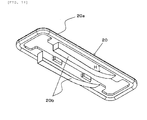
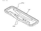
- the flow passage control member be arranged such that a minimum distance between the flow passage control member and the group of radiator fins is set equal to or less than a distance between the fins of the group of radiator fins.
- the flow passage control member in the power conversion device of the first or the second aspect, it is preferable that the flow passage control member be continuously distributed in the gap along the flow direction of the cooling medium.
- the flow passage control member in the power conversion device of the third aspect, it is preferable that the flow passage control member have a shape by which the distance between the flow passage control member and the group of radiator fins is decreased along the flow direction of the cooling medium.
- the generated AC power is converted into DC power by a power conversion device 200 as described later, a high-voltage battery 136 is charged with DC power, and charged electric power is used as energy for traveling of a vehicle again.
- electric power which is stored in the high-voltage battery 136 becomes small, rotational energy generated by the engine EGN is converted into AC power using the motor generator MG2.
- the battery 136 can be charged with DC power.
- the transmission of kinetic energy from the engine EGN to the motor generator MG2 is performed by the power distribution mechanism TSM.
- the constitutions of electric circuits of the inverter circuit 140 and the inverter circuit 142 are explained in conjunction with Fig. 2 .
- the inverter circuit 140 and the inverter circuit 142 are extremely similar to each other with respect to the circuit constitution and the manner of operation and hence, the explanation is made hereinafter by taking the inverter circuit 140 as a representing example. Further, in the explanation made hereinafter, an insulated-gate bipolar transistor is used as a semiconductor element, and the insulated-gate bipolar transistor is abbreviated as IGBT hereinafter.
- a metal oxide semiconductor field effect transistor (abbreviated as MOSFET hereinafter) may be used as a switching power semiconductor element.
- MOSFET metal oxide semiconductor field effect transistor
- the diode 156 and the diode 166 become unnecessary.
- an IGBT is suitable for a case where a DC voltage is relatively high
- a MOSFET is suitable for a case where a DC voltage is relatively low.
- the micon generates a pulse-shaped modulated wave based on a comparison between a fundamental wave (sinusoidal wave) based on the voltage command values of the U phase, the V phase and the W phase and a carrier wave (triangular wave), and outputs the generated modulated wave to the driver circuit 174 as a PWM (pulse width modulation) signal.
- a fundamental wave sinusoidal wave
- a carrier wave triangular wave
- the driver circuit 174 in driving the lower arm, outputs a drive signal obtained by amplifying the PWM signal to a gate electrode of the IGBT 330 of the corresponding lower arm.
- the driver circuit 174 in driving the upper arm, amplifies a PWM signal after shifting a level of a reference potential of the PWM signal to a level of a reference potential of the upper arm, and outputs the amplified PWM signal to a gate electrode of the IGBT 328 of the corresponding upper arm as a drive signal.
- Information on the temperature of the series circuit of upper and lower arms 150 is inputted to the micon from a temperature sensor (not shown in the drawing) mounted in the series circuit of upper and lower arms 150. Further, information on a voltage on a DC positive pole side of the series circuit of upper and lower arms 150 is inputted in the micon. The micon performs the overtemperature detection and the overvoltage detection based on these information, and stops the switching operations of all IGBTs 328 and IGBTs 330 when an overtemperature or an overvoltage is detected.
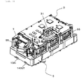
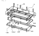
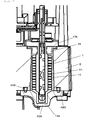
- Fig. 3 to Fig. 5 are views showing the schematic constitution of the power conversion device 200 according to this embodiment, wherein Fig. 3 is a perspective view of the power conversion device 200, Fig. 4 is an exploded perspective view of the power conversion device 200, and Fig. 5 is a cross-sectional view taken along a line A-A in Fig. 3 .
- a shape of the power conversion device 200 as viewed in a plan view is formed into an approximately rectangular shape so that the power conversion device 200 can acquire advantageous effects that the power conversion device 200 can be easily mounted on a vehicle, and can be easily manufactured.
- the power conversion device 200 includes: a cooling base 5 in which the capacitor module 500 and a power modules 1 are housed; and a drive circuit board 2, a control circuit board 3 and the like which are arranged over the cooling base 5.
- the above-mentioned control circuit 172 is mounted on the control circuit board 3.
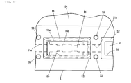
- a flow passage 51 through which a cooling medium flows, and a capacitor housing portion 54 which is formed such that the capacitor housing portion 54 is surrounded by the flow passage 51 are formed.
- the capacitor module 500 is housed in the capacitor housing portion 54, and is cooled through a wall surface of the flow passage 51.
- a plurality of opening portions 50 are formed in the cooling base 5 along the flow passage 51.
- the power module 1 is constituted such that the above-mentioned series circuit of upper and lower arms 150 is housed in the inside of a metal casing, and generates the largest heat value among the electronic parts. Accordingly, the plurality of power modules 1 are inserted into the inside of the flow passage 51 through the opening portions 50 and are directly cooled by a cooling medium.
- An inlet port 13IN and a discharge port 14OUT are formed in a bottom portion of the cooling base 5.
- a cooling medium for example, cooling water flows into the inside of the flow passage 51 through the inlet port 13IN, circulates in the flow passage 51 and, thereafter, is flown out from the discharge port 14OUT.
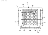
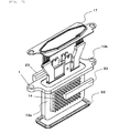
- Fig. 7 is a view showing a part of the cross-sectional view shown in Fig. 4 in such a manner that a portion of the flow passage portion in which the power modules 1 are housed is shown in an enlarged manner.
- An opening of the flow passage 51 which is formed in the cooling base 5 on a base back surface side is hermetically closed by the lower cover 420.
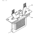
- a cylindrical portion on which radiator fins 14 are formed is inserted into the flow passage 51 through the opening portion 50 (see Fig. 5 ) and a flange portion 13b is fixed to an upper surface of the cooling base 5.
- the casing 13 is, for reducing a manufacturing cost, formed of an integral-body-type vessel which is formed in such a manner that the forming of the casing 13 into a can shape, the forming of the radiator fins 14, and the forming of the flange portion 13b are performed by forging.
- a gap of approximately 5 to 10 mm is formed between the flange portion 13b and the radiator fins 14.
- the radiator fins 14 and the flange portion 13b may be formed by cutting. Also in this case, a gap into which a tool enters is necessary at the time of cutting a sealing surface of the flange portion 13b and hence, a gap is formed between the flange portion 13b and the radiator fins 14.
- the double-dashed chained line 144 indicates a group of radiator fins.
- a recessed portion is formed on the lower cover 420 which constitutes a bottom surface of the flow passage 51 in a state where the recessed portion conforms to a bottom surface of the power module 1 in shape thus preventing the formation of a space on a bottom surface side through which a cooling medium bypasses.
Landscapes
- Engineering & Computer Science (AREA)
- Power Engineering (AREA)
- Physics & Mathematics (AREA)
- Thermal Sciences (AREA)
- Microelectronics & Electronic Packaging (AREA)
- Inverter Devices (AREA)
- Cooling Or The Like Of Semiconductors Or Solid State Devices (AREA)
Applications Claiming Priority (2)
| Application Number | Priority Date | Filing Date | Title |
|---|---|---|---|
| JP2010168813A JP5439309B2 (ja) | 2010-07-28 | 2010-07-28 | 電力変換装置 |
| PCT/JP2011/066853 WO2012014842A1 (fr) | 2010-07-28 | 2011-07-25 | Convertisseur de puissance |
Publications (3)
| Publication Number | Publication Date |
|---|---|
| EP2600516A1 true EP2600516A1 (fr) | 2013-06-05 |
| EP2600516A4 EP2600516A4 (fr) | 2018-01-24 |
| EP2600516B1 EP2600516B1 (fr) | 2020-09-30 |
Family
ID=45530050
Family Applications (1)
| Application Number | Title | Priority Date | Filing Date |
|---|---|---|---|
| EP11812431.2A Active EP2600516B1 (fr) | 2010-07-28 | 2011-07-25 | Convertisseur de puissance |
Country Status (5)
| Country | Link |
|---|---|
| US (1) | US9078376B2 (fr) |
| EP (1) | EP2600516B1 (fr) |
| JP (1) | JP5439309B2 (fr) |
| CN (1) | CN103026605B (fr) |
| WO (1) | WO2012014842A1 (fr) |
Families Citing this family (28)
| Publication number | Priority date | Publication date | Assignee | Title |
|---|---|---|---|---|
| JP5370448B2 (ja) * | 2011-09-19 | 2013-12-18 | 株式会社デンソー | 電力変換装置 |
| JP5949286B2 (ja) * | 2012-07-31 | 2016-07-06 | 株式会社デンソー | 電力変換装置 |
| JP2014072395A (ja) | 2012-09-28 | 2014-04-21 | Toyota Industries Corp | 冷却装置 |
| JP6262422B2 (ja) | 2012-10-02 | 2018-01-17 | 昭和電工株式会社 | 冷却装置および半導体装置 |
| US9204573B2 (en) * | 2013-05-08 | 2015-12-01 | Kabushiki Kaisha Toshiba | Power conversion apparatus |
| JP6101609B2 (ja) * | 2013-09-20 | 2017-03-22 | 日立オートモティブシステムズ株式会社 | パワー半導体モジュール及びそれを用いた電力変換装置 |
| US9992915B2 (en) | 2013-10-07 | 2018-06-05 | Hitachi Automotive Systems, Ltd. | Power conversion device |
| US20150138734A1 (en) * | 2013-11-18 | 2015-05-21 | Magna Electronics Inc. | 360 degree direct cooled power module |
| JP6193173B2 (ja) * | 2014-04-17 | 2017-09-06 | 日立オートモティブシステムズ株式会社 | 電力変換装置 |
| WO2015198411A1 (fr) * | 2014-06-25 | 2015-12-30 | 株式会社日立製作所 | Dispositif de module de puissance, dispositif de conversion de puissance et procédé de fabrication de dispositif de module de puissance |
| DE112015002587B4 (de) * | 2014-06-26 | 2021-04-15 | Hitachi Automotive Systems, Ltd. | Leistungshalbleitermodul und herstellungsverfahren des leistungshalbleitermoduls |
| JP6302803B2 (ja) * | 2014-09-09 | 2018-03-28 | 日立オートモティブシステムズ株式会社 | パワー半導体モジュール及びその製造方法、電力変換装置 |
| US10037952B2 (en) * | 2015-02-10 | 2018-07-31 | Mediatek Inc. | Integrated circuit, electronic device and method for transmitting data in electronic device |
| US9978692B2 (en) * | 2015-02-10 | 2018-05-22 | Mediatek Inc. | Integrated circuit, electronic device and method for transmitting data in electronic device |
| WO2017033295A1 (fr) * | 2015-08-26 | 2017-03-02 | 日立オートモティブシステムズ株式会社 | Structure |
| JP6593221B2 (ja) * | 2016-02-23 | 2019-10-23 | 株式会社デンソー | 電力変換装置 |
| WO2017149801A1 (fr) * | 2016-03-02 | 2017-09-08 | 三菱電機株式会社 | Dispositif de conversion de puissance |
| WO2017187781A1 (fr) * | 2016-04-28 | 2017-11-02 | 日立オートモティブシステムズ株式会社 | Dispositif de conversion de courant |
| JP7264159B2 (ja) * | 2018-04-06 | 2023-04-25 | ニデック株式会社 | 電力変換装置 |
| JP7159620B2 (ja) * | 2018-05-30 | 2022-10-25 | 富士電機株式会社 | 半導体装置、冷却モジュール、電力変換装置及び電動車両 |
| JP7208757B2 (ja) * | 2018-10-03 | 2023-01-19 | 川崎重工業株式会社 | 制御装置 |
| JP7233014B2 (ja) * | 2018-12-26 | 2023-03-06 | パナソニックIpマネジメント株式会社 | 電力変換装置 |
| JP6777203B2 (ja) * | 2019-08-09 | 2020-10-28 | 株式会社デンソー | 電力変換装置 |
| JP2022188312A (ja) * | 2019-11-27 | 2022-12-21 | 日立Astemo株式会社 | パワーモジュールおよびパワーモジュールの製造方法 |
| JP7419050B2 (ja) | 2019-12-16 | 2024-01-22 | 日立Astemo株式会社 | パワーモジュール、電力変換装置、およびパワーモジュールの製造方法 |
| JP7294455B2 (ja) * | 2019-12-19 | 2023-06-20 | 東芝三菱電機産業システム株式会社 | 電力変換装置およびその製造方法 |
| KR102810533B1 (ko) * | 2020-02-28 | 2025-05-22 | 현대모비스 주식회사 | 전력변환장치의 냉각구조체 |
| CN112053999B (zh) * | 2020-08-10 | 2022-05-13 | 浙江艾罗网络能源技术股份有限公司 | 一种用于固定逆变器晶体管的高强度绝缘压块 |
Family Cites Families (9)
| Publication number | Priority date | Publication date | Assignee | Title |
|---|---|---|---|---|
| JPH02210899A (ja) * | 1989-02-09 | 1990-08-22 | Fujitsu Ltd | 印刷配線板ユニットの冷却構造 |
| DE19643717A1 (de) * | 1996-10-23 | 1998-04-30 | Asea Brown Boveri | Flüssigkeits-Kühlvorrichtung für ein Hochleistungshalbleitermodul |
| JP4168825B2 (ja) | 2003-05-07 | 2008-10-22 | トヨタ自動車株式会社 | 半導体モジュールおよび半導体モジュールを搭載した半導体モジュールユニット |
| US6992382B2 (en) * | 2003-12-29 | 2006-01-31 | Intel Corporation | Integrated micro channels and manifold/plenum using separate silicon or low-cost polycrystalline silicon |
| JP2005348533A (ja) * | 2004-06-03 | 2005-12-15 | Fuji Electric Fa Components & Systems Co Ltd | インバータ装置 |
| JP5120605B2 (ja) * | 2007-05-22 | 2013-01-16 | アイシン・エィ・ダブリュ株式会社 | 半導体モジュール及びインバータ装置 |
| TWI423403B (zh) * | 2007-09-17 | 2014-01-11 | 萬國商業機器公司 | 積體電路疊層 |
| JP5557441B2 (ja) * | 2008-10-31 | 2014-07-23 | 日立オートモティブシステムズ株式会社 | 電力変換装置および電動車両 |
| US8064198B2 (en) * | 2009-06-29 | 2011-11-22 | Honda Motor Co., Ltd. | Cooling device for semiconductor element module and magnetic part |
-
2010
- 2010-07-28 JP JP2010168813A patent/JP5439309B2/ja active Active
-
2011
- 2011-07-25 EP EP11812431.2A patent/EP2600516B1/fr active Active
- 2011-07-25 CN CN201180036876.6A patent/CN103026605B/zh active Active
- 2011-07-25 WO PCT/JP2011/066853 patent/WO2012014842A1/fr not_active Ceased
- 2011-07-25 US US13/811,497 patent/US9078376B2/en active Active
Non-Patent Citations (1)
| Title |
|---|
| See references of WO2012014842A1 * |
Also Published As
| Publication number | Publication date |
|---|---|
| CN103026605A (zh) | 2013-04-03 |
| EP2600516A4 (fr) | 2018-01-24 |
| JP2012029539A (ja) | 2012-02-09 |
| US9078376B2 (en) | 2015-07-07 |
| WO2012014842A1 (fr) | 2012-02-02 |
| EP2600516B1 (fr) | 2020-09-30 |
| JP5439309B2 (ja) | 2014-03-12 |
| US20130128646A1 (en) | 2013-05-23 |
| CN103026605B (zh) | 2015-09-09 |
Similar Documents
| Publication | Publication Date | Title |
|---|---|---|
| EP2600516B1 (fr) | Convertisseur de puissance | |
| JP5851372B2 (ja) | 電力変換装置 | |
| JP5508357B2 (ja) | 電力変換装置 | |
| JP4452953B2 (ja) | 電力変換装置 | |
| JP5422466B2 (ja) | 電力変換装置 | |
| US8659130B2 (en) | Power module and power module manufacturing method | |
| US9474191B2 (en) | Power semiconductor module | |
| US9419535B2 (en) | Electric power converter | |
| JP5815063B2 (ja) | 電力変換装置 | |
| WO2011162241A1 (fr) | Dispositif de conversion de puissance | |
| JP2011217550A (ja) | 電力変換装置 | |
| JP2010245910A (ja) | 電力変換装置及びそれを用いた車載用電機システム | |
| WO2014034331A1 (fr) | Appareil de conversion de puissance | |
| JP2013005067A (ja) | 電力変換装置 | |
| WO2021225072A1 (fr) | Dispositif de conversion d'énergie | |
| JP2010011671A (ja) | 電力変換装置 | |
| JP5623985B2 (ja) | 電力変換装置 | |
| JP2014166043A (ja) | 電力変換装置 | |
| JP2010110066A (ja) | 電力変換装置 | |
| JP6272064B2 (ja) | 電力変換装置 |
Legal Events
| Date | Code | Title | Description |
|---|---|---|---|
| PUAI | Public reference made under article 153(3) epc to a published international application that has entered the european phase |
Free format text: ORIGINAL CODE: 0009012 |
|
| 17P | Request for examination filed |
Effective date: 20130228 |
|
| AK | Designated contracting states |
Kind code of ref document: A1 Designated state(s): AL AT BE BG CH CY CZ DE DK EE ES FI FR GB GR HR HU IE IS IT LI LT LU LV MC MK MT NL NO PL PT RO RS SE SI SK SM TR |
|
| DAX | Request for extension of the european patent (deleted) | ||
| RA4 | Supplementary search report drawn up and despatched (corrected) |
Effective date: 20180102 |
|
| RIC1 | Information provided on ipc code assigned before grant |
Ipc: H01L 25/07 20060101ALI20171219BHEP Ipc: H01L 23/367 20060101ALI20171219BHEP Ipc: H01L 23/473 20060101ALI20171219BHEP Ipc: H01L 25/18 20060101ALI20171219BHEP Ipc: H02M 7/48 20070101AFI20171219BHEP |
|
| GRAP | Despatch of communication of intention to grant a patent |
Free format text: ORIGINAL CODE: EPIDOSNIGR1 |
|
| STAA | Information on the status of an ep patent application or granted ep patent |
Free format text: STATUS: GRANT OF PATENT IS INTENDED |
|
| INTG | Intention to grant announced |
Effective date: 20200402 |
|
| GRAJ | Information related to disapproval of communication of intention to grant by the applicant or resumption of examination proceedings by the epo deleted |
Free format text: ORIGINAL CODE: EPIDOSDIGR1 |
|
| STAA | Information on the status of an ep patent application or granted ep patent |
Free format text: STATUS: REQUEST FOR EXAMINATION WAS MADE |
|
| GRAP | Despatch of communication of intention to grant a patent |
Free format text: ORIGINAL CODE: EPIDOSNIGR1 |
|
| STAA | Information on the status of an ep patent application or granted ep patent |
Free format text: STATUS: GRANT OF PATENT IS INTENDED |
|
| INTC | Intention to grant announced (deleted) | ||
| INTG | Intention to grant announced |
Effective date: 20200713 |
|
| GRAS | Grant fee paid |
Free format text: ORIGINAL CODE: EPIDOSNIGR3 |
|
| GRAA | (expected) grant |
Free format text: ORIGINAL CODE: 0009210 |
|
| STAA | Information on the status of an ep patent application or granted ep patent |
Free format text: STATUS: THE PATENT HAS BEEN GRANTED |
|
| AK | Designated contracting states |
Kind code of ref document: B1 Designated state(s): AL AT BE BG CH CY CZ DE DK EE ES FI FR GB GR HR HU IE IS IT LI LT LU LV MC MK MT NL NO PL PT RO RS SE SI SK SM TR |
|
| REG | Reference to a national code |
Ref country code: CH Ref legal event code: EP Ref country code: GB Ref legal event code: FG4D |
|
| REG | Reference to a national code |
Ref country code: DE Ref legal event code: R096 Ref document number: 602011068786 Country of ref document: DE Ref country code: AT Ref legal event code: REF Ref document number: 1319834 Country of ref document: AT Kind code of ref document: T Effective date: 20201015 |
|
| REG | Reference to a national code |
Ref country code: IE Ref legal event code: FG4D |
|
| PG25 | Lapsed in a contracting state [announced via postgrant information from national office to epo] |
Ref country code: SE Free format text: LAPSE BECAUSE OF FAILURE TO SUBMIT A TRANSLATION OF THE DESCRIPTION OR TO PAY THE FEE WITHIN THE PRESCRIBED TIME-LIMIT Effective date: 20200930 Ref country code: BG Free format text: LAPSE BECAUSE OF FAILURE TO SUBMIT A TRANSLATION OF THE DESCRIPTION OR TO PAY THE FEE WITHIN THE PRESCRIBED TIME-LIMIT Effective date: 20201230 Ref country code: FI Free format text: LAPSE BECAUSE OF FAILURE TO SUBMIT A TRANSLATION OF THE DESCRIPTION OR TO PAY THE FEE WITHIN THE PRESCRIBED TIME-LIMIT Effective date: 20200930 Ref country code: GR Free format text: LAPSE BECAUSE OF FAILURE TO SUBMIT A TRANSLATION OF THE DESCRIPTION OR TO PAY THE FEE WITHIN THE PRESCRIBED TIME-LIMIT Effective date: 20201231 Ref country code: NO Free format text: LAPSE BECAUSE OF FAILURE TO SUBMIT A TRANSLATION OF THE DESCRIPTION OR TO PAY THE FEE WITHIN THE PRESCRIBED TIME-LIMIT Effective date: 20201230 Ref country code: HR Free format text: LAPSE BECAUSE OF FAILURE TO SUBMIT A TRANSLATION OF THE DESCRIPTION OR TO PAY THE FEE WITHIN THE PRESCRIBED TIME-LIMIT Effective date: 20200930 |
|
| REG | Reference to a national code |
Ref country code: AT Ref legal event code: MK05 Ref document number: 1319834 Country of ref document: AT Kind code of ref document: T Effective date: 20200930 |
|
| PG25 | Lapsed in a contracting state [announced via postgrant information from national office to epo] |
Ref country code: LV Free format text: LAPSE BECAUSE OF FAILURE TO SUBMIT A TRANSLATION OF THE DESCRIPTION OR TO PAY THE FEE WITHIN THE PRESCRIBED TIME-LIMIT Effective date: 20200930 Ref country code: RS Free format text: LAPSE BECAUSE OF FAILURE TO SUBMIT A TRANSLATION OF THE DESCRIPTION OR TO PAY THE FEE WITHIN THE PRESCRIBED TIME-LIMIT Effective date: 20200930 |
|
| REG | Reference to a national code |
Ref country code: NL Ref legal event code: MP Effective date: 20200930 |
|
| REG | Reference to a national code |
Ref country code: DE Ref legal event code: R082 Ref document number: 602011068786 Country of ref document: DE Representative=s name: MERH-IP MATIAS ERNY REICHL HOFFMANN PATENTANWA, DE Ref country code: DE Ref legal event code: R081 Ref document number: 602011068786 Country of ref document: DE Owner name: HITACHI ASTEMO, LTD., HITACHINAKA-SHI, JP Free format text: FORMER OWNER: HITACHI AUTOMOTIVE SYSTEMS, LTD., HITACHINAKA-SHI, IBARAKI, JP |
|
| REG | Reference to a national code |
Ref country code: LT Ref legal event code: MG4D |
|
| PG25 | Lapsed in a contracting state [announced via postgrant information from national office to epo] |
Ref country code: LT Free format text: LAPSE BECAUSE OF FAILURE TO SUBMIT A TRANSLATION OF THE DESCRIPTION OR TO PAY THE FEE WITHIN THE PRESCRIBED TIME-LIMIT Effective date: 20200930 Ref country code: PT Free format text: LAPSE BECAUSE OF FAILURE TO SUBMIT A TRANSLATION OF THE DESCRIPTION OR TO PAY THE FEE WITHIN THE PRESCRIBED TIME-LIMIT Effective date: 20210201 Ref country code: NL Free format text: LAPSE BECAUSE OF FAILURE TO SUBMIT A TRANSLATION OF THE DESCRIPTION OR TO PAY THE FEE WITHIN THE PRESCRIBED TIME-LIMIT Effective date: 20200930 Ref country code: RO Free format text: LAPSE BECAUSE OF FAILURE TO SUBMIT A TRANSLATION OF THE DESCRIPTION OR TO PAY THE FEE WITHIN THE PRESCRIBED TIME-LIMIT Effective date: 20200930 Ref country code: SM Free format text: LAPSE BECAUSE OF FAILURE TO SUBMIT A TRANSLATION OF THE DESCRIPTION OR TO PAY THE FEE WITHIN THE PRESCRIBED TIME-LIMIT Effective date: 20200930 Ref country code: CZ Free format text: LAPSE BECAUSE OF FAILURE TO SUBMIT A TRANSLATION OF THE DESCRIPTION OR TO PAY THE FEE WITHIN THE PRESCRIBED TIME-LIMIT Effective date: 20200930 Ref country code: EE Free format text: LAPSE BECAUSE OF FAILURE TO SUBMIT A TRANSLATION OF THE DESCRIPTION OR TO PAY THE FEE WITHIN THE PRESCRIBED TIME-LIMIT Effective date: 20200930 |
|
| PG25 | Lapsed in a contracting state [announced via postgrant information from national office to epo] |
Ref country code: AT Free format text: LAPSE BECAUSE OF FAILURE TO SUBMIT A TRANSLATION OF THE DESCRIPTION OR TO PAY THE FEE WITHIN THE PRESCRIBED TIME-LIMIT Effective date: 20200930 Ref country code: AL Free format text: LAPSE BECAUSE OF FAILURE TO SUBMIT A TRANSLATION OF THE DESCRIPTION OR TO PAY THE FEE WITHIN THE PRESCRIBED TIME-LIMIT Effective date: 20200930 Ref country code: ES Free format text: LAPSE BECAUSE OF FAILURE TO SUBMIT A TRANSLATION OF THE DESCRIPTION OR TO PAY THE FEE WITHIN THE PRESCRIBED TIME-LIMIT Effective date: 20200930 Ref country code: IS Free format text: LAPSE BECAUSE OF FAILURE TO SUBMIT A TRANSLATION OF THE DESCRIPTION OR TO PAY THE FEE WITHIN THE PRESCRIBED TIME-LIMIT Effective date: 20210130 Ref country code: PL Free format text: LAPSE BECAUSE OF FAILURE TO SUBMIT A TRANSLATION OF THE DESCRIPTION OR TO PAY THE FEE WITHIN THE PRESCRIBED TIME-LIMIT Effective date: 20200930 |
|
| PG25 | Lapsed in a contracting state [announced via postgrant information from national office to epo] |
Ref country code: SK Free format text: LAPSE BECAUSE OF FAILURE TO SUBMIT A TRANSLATION OF THE DESCRIPTION OR TO PAY THE FEE WITHIN THE PRESCRIBED TIME-LIMIT Effective date: 20200930 |
|
| REG | Reference to a national code |
Ref country code: DE Ref legal event code: R097 Ref document number: 602011068786 Country of ref document: DE |
|
| PLBE | No opposition filed within time limit |
Free format text: ORIGINAL CODE: 0009261 |
|
| STAA | Information on the status of an ep patent application or granted ep patent |
Free format text: STATUS: NO OPPOSITION FILED WITHIN TIME LIMIT |
|
| PG25 | Lapsed in a contracting state [announced via postgrant information from national office to epo] |
Ref country code: DK Free format text: LAPSE BECAUSE OF FAILURE TO SUBMIT A TRANSLATION OF THE DESCRIPTION OR TO PAY THE FEE WITHIN THE PRESCRIBED TIME-LIMIT Effective date: 20200930 |
|
| 26N | No opposition filed |
Effective date: 20210701 |
|
| PG25 | Lapsed in a contracting state [announced via postgrant information from national office to epo] |
Ref country code: IT Free format text: LAPSE BECAUSE OF FAILURE TO SUBMIT A TRANSLATION OF THE DESCRIPTION OR TO PAY THE FEE WITHIN THE PRESCRIBED TIME-LIMIT Effective date: 20200930 |
|
| PG25 | Lapsed in a contracting state [announced via postgrant information from national office to epo] |
Ref country code: SI Free format text: LAPSE BECAUSE OF FAILURE TO SUBMIT A TRANSLATION OF THE DESCRIPTION OR TO PAY THE FEE WITHIN THE PRESCRIBED TIME-LIMIT Effective date: 20200930 |
|
| REG | Reference to a national code |
Ref country code: CH Ref legal event code: PL |
|
| GBPC | Gb: european patent ceased through non-payment of renewal fee |
Effective date: 20210725 |
|
| PG25 | Lapsed in a contracting state [announced via postgrant information from national office to epo] |
Ref country code: MC Free format text: LAPSE BECAUSE OF FAILURE TO SUBMIT A TRANSLATION OF THE DESCRIPTION OR TO PAY THE FEE WITHIN THE PRESCRIBED TIME-LIMIT Effective date: 20200930 |
|
| REG | Reference to a national code |
Ref country code: BE Ref legal event code: MM Effective date: 20210731 |
|
| PG25 | Lapsed in a contracting state [announced via postgrant information from national office to epo] |
Ref country code: LI Free format text: LAPSE BECAUSE OF NON-PAYMENT OF DUE FEES Effective date: 20210731 Ref country code: GB Free format text: LAPSE BECAUSE OF NON-PAYMENT OF DUE FEES Effective date: 20210725 Ref country code: CH Free format text: LAPSE BECAUSE OF NON-PAYMENT OF DUE FEES Effective date: 20210731 |
|
| PG25 | Lapsed in a contracting state [announced via postgrant information from national office to epo] |
Ref country code: IS Free format text: LAPSE BECAUSE OF FAILURE TO SUBMIT A TRANSLATION OF THE DESCRIPTION OR TO PAY THE FEE WITHIN THE PRESCRIBED TIME-LIMIT Effective date: 20210130 Ref country code: LU Free format text: LAPSE BECAUSE OF NON-PAYMENT OF DUE FEES Effective date: 20210725 Ref country code: FR Free format text: LAPSE BECAUSE OF NON-PAYMENT OF DUE FEES Effective date: 20210731 |
|
| PG25 | Lapsed in a contracting state [announced via postgrant information from national office to epo] |
Ref country code: IE Free format text: LAPSE BECAUSE OF NON-PAYMENT OF DUE FEES Effective date: 20210725 Ref country code: BE Free format text: LAPSE BECAUSE OF NON-PAYMENT OF DUE FEES Effective date: 20210731 |
|
| PG25 | Lapsed in a contracting state [announced via postgrant information from national office to epo] |
Ref country code: HU Free format text: LAPSE BECAUSE OF FAILURE TO SUBMIT A TRANSLATION OF THE DESCRIPTION OR TO PAY THE FEE WITHIN THE PRESCRIBED TIME-LIMIT; INVALID AB INITIO Effective date: 20110725 Ref country code: CY Free format text: LAPSE BECAUSE OF FAILURE TO SUBMIT A TRANSLATION OF THE DESCRIPTION OR TO PAY THE FEE WITHIN THE PRESCRIBED TIME-LIMIT Effective date: 20200930 |
|
| PG25 | Lapsed in a contracting state [announced via postgrant information from national office to epo] |
Ref country code: MK Free format text: LAPSE BECAUSE OF FAILURE TO SUBMIT A TRANSLATION OF THE DESCRIPTION OR TO PAY THE FEE WITHIN THE PRESCRIBED TIME-LIMIT Effective date: 20200930 |
|
| PG25 | Lapsed in a contracting state [announced via postgrant information from national office to epo] |
Ref country code: MT Free format text: LAPSE BECAUSE OF FAILURE TO SUBMIT A TRANSLATION OF THE DESCRIPTION OR TO PAY THE FEE WITHIN THE PRESCRIBED TIME-LIMIT Effective date: 20200930 |
|
| PGFP | Annual fee paid to national office [announced via postgrant information from national office to epo] |
Ref country code: DE Payment date: 20250528 Year of fee payment: 15 |
|
| PG25 | Lapsed in a contracting state [announced via postgrant information from national office to epo] |
Ref country code: TR Free format text: LAPSE BECAUSE OF FAILURE TO SUBMIT A TRANSLATION OF THE DESCRIPTION OR TO PAY THE FEE WITHIN THE PRESCRIBED TIME-LIMIT Effective date: 20200930 |