EP2600516B1 - Stromwandler - Google Patents
Stromwandler Download PDFInfo
- Publication number
- EP2600516B1 EP2600516B1 EP11812431.2A EP11812431A EP2600516B1 EP 2600516 B1 EP2600516 B1 EP 2600516B1 EP 11812431 A EP11812431 A EP 11812431A EP 2600516 B1 EP2600516 B1 EP 2600516B1
- Authority
- EP
- European Patent Office
- Prior art keywords
- flow passage
- power
- passage control
- control member
- group
- Prior art date
- Legal status (The legal status is an assumption and is not a legal conclusion. Google has not performed a legal analysis and makes no representation as to the accuracy of the status listed.)
- Active
Links
Images









Classifications
-
- H—ELECTRICITY
- H05—ELECTRIC TECHNIQUES NOT OTHERWISE PROVIDED FOR
- H05K—PRINTED CIRCUITS; CASINGS OR CONSTRUCTIONAL DETAILS OF ELECTRIC APPARATUS; MANUFACTURE OF ASSEMBLAGES OF ELECTRICAL COMPONENTS
- H05K7/00—Constructional details common to different types of electric apparatus
- H05K7/20—Modifications to facilitate cooling, ventilating, or heating
-
- H—ELECTRICITY
- H02—GENERATION; CONVERSION OR DISTRIBUTION OF ELECTRIC POWER
- H02M—APPARATUS FOR CONVERSION BETWEEN AC AND AC, BETWEEN AC AND DC, OR BETWEEN DC AND DC, AND FOR USE WITH MAINS OR SIMILAR POWER SUPPLY SYSTEMS; CONVERSION OF DC OR AC INPUT POWER INTO SURGE OUTPUT POWER; CONTROL OR REGULATION THEREOF
- H02M7/00—Conversion of AC power input into DC power output; Conversion of DC power input into AC power output
- H02M7/003—Constructional details, e.g. physical layout, assembly, wiring or busbar connections
-
- H—ELECTRICITY
- H10—SEMICONDUCTOR DEVICES; ELECTRIC SOLID-STATE DEVICES NOT OTHERWISE PROVIDED FOR
- H10W—GENERIC PACKAGES, INTERCONNECTIONS, CONNECTORS OR OTHER CONSTRUCTIONAL DETAILS OF DEVICES COVERED BY CLASS H10
- H10W40/00—Arrangements for thermal protection or thermal control
- H10W40/20—Arrangements for cooling
- H10W40/22—Arrangements for cooling characterised by their shape, e.g. having conical or cylindrical projections
-
- H—ELECTRICITY
- H10—SEMICONDUCTOR DEVICES; ELECTRIC SOLID-STATE DEVICES NOT OTHERWISE PROVIDED FOR
- H10W—GENERIC PACKAGES, INTERCONNECTIONS, CONNECTORS OR OTHER CONSTRUCTIONAL DETAILS OF DEVICES COVERED BY CLASS H10
- H10W40/00—Arrangements for thermal protection or thermal control
- H10W40/40—Arrangements for thermal protection or thermal control involving heat exchange by flowing fluids
- H10W40/47—Arrangements for thermal protection or thermal control involving heat exchange by flowing fluids by flowing liquids, e.g. forced water cooling
-
- H—ELECTRICITY
- H02—GENERATION; CONVERSION OR DISTRIBUTION OF ELECTRIC POWER
- H02M—APPARATUS FOR CONVERSION BETWEEN AC AND AC, BETWEEN AC AND DC, OR BETWEEN DC AND DC, AND FOR USE WITH MAINS OR SIMILAR POWER SUPPLY SYSTEMS; CONVERSION OF DC OR AC INPUT POWER INTO SURGE OUTPUT POWER; CONTROL OR REGULATION THEREOF
- H02M7/00—Conversion of AC power input into DC power output; Conversion of DC power input into AC power output
- H02M7/42—Conversion of DC power input into AC power output without possibility of reversal
- H02M7/44—Conversion of DC power input into AC power output without possibility of reversal by static converters
- H02M7/48—Conversion of DC power input into AC power output without possibility of reversal by static converters using discharge tubes with control electrode or semiconductor devices with control electrode
-
- H—ELECTRICITY
- H10—SEMICONDUCTOR DEVICES; ELECTRIC SOLID-STATE DEVICES NOT OTHERWISE PROVIDED FOR
- H10W—GENERIC PACKAGES, INTERCONNECTIONS, CONNECTORS OR OTHER CONSTRUCTIONAL DETAILS OF DEVICES COVERED BY CLASS H10
- H10W42/00—Arrangements for protection of devices
- H10W42/20—Arrangements for protection of devices protecting against electromagnetic or particle radiation, e.g. light, X-rays, gamma-rays or electrons
-
- H—ELECTRICITY
- H10—SEMICONDUCTOR DEVICES; ELECTRIC SOLID-STATE DEVICES NOT OTHERWISE PROVIDED FOR
- H10W—GENERIC PACKAGES, INTERCONNECTIONS, CONNECTORS OR OTHER CONSTRUCTIONAL DETAILS OF DEVICES COVERED BY CLASS H10
- H10W90/00—Package configurations
Definitions
- the present invention relates to a power conversion device.
- An electric automobile or a hybrid automobile mounts a motor as a power source for a vehicle thereon, and includes a power conversion device such as an inverter for controlling electric power to be supplied to the motor.
- the power conversion device includes a power module which incorporates a power semiconductor element such as an IGBT therein, a drive circuit which drives the power module, a control circuit for controlling these parts, and a current smoothing capacitor. Since these electronic parts are weak with respect to heat, it is necessary to cool these parts. In many cases, a large-capacity power conversion device with a large heat value is provided with a cooler having the water cooler structure for circulating cooling water therein.
- the power module is the part which has the largest heat value.
- the double-sided cooling structure which simultaneously cools both surfaces of the semiconductor element is effective.
- the double-sided cooling mounting structure of the power module there has been known the structure described in patent literature 1.
- Document JP 2010 110143 A describes a power converter with a first flow path forming body and a second flow path forming body for receiving a power semiconductor module according to the preamble of claim 1.
- Document JP 2005 348533 A describes an inverter device and a structure for cooling a semiconductor element of the inverter device.
- Document JP 2-210899 A describes a cooling structure with a fan for cooling a printed wiring board unit.
- a power conversion device which includes: a flow passage casing in which a flow passage through which a cooling medium flows is formed and an opening portion which is communicated with the flow passage is formed; a power module having a bottomed cylindrical portion in which a power semiconductor element is housed and which is inserted into the flow passage through the opening portion, a flange portion which is formed on an opening of the cylindrical portion and is fixed to the flow passage casing so as to close the opening portion, and a group of radiator fins which are mounted on an outer peripheral surface of the cylindrical portion with a gap of a predetermined distance formed between the flange portion and the group of radiator fins; and a flow passage control member which is arranged in a gap formed between the flange portion and the group of radiator fins, and introduces the cooling medium into the group of radiator fins, wherein power is converted into AC power from DC power or into DC power from AC power by a switching operation of the power semiconductor element.
- the flow passage control member be arranged such that a minimum distance between the flow passage control member and the group of radiator fins is set equal to or less than a distance between the fins of the group of radiator fins.
- the flow passage control member be continuously distributed in the gap along the flow direction of the cooling medium.
- the flow passage control member in the power conversion device of the third aspect, it is preferable that the flow passage control member have a shape by which the distance between the flow passage control member and the group of radiator fins is decreased along the flow direction of the cooling medium.
- the flow passage control member have a shape by which the distance between the flow passage control member and the group of radiator fins becomes minimum at the center in the flow direction of the group of radiator fins, and the distance is gradually increased in terms of being further away from the center in the flow direction.
- the flow passage control member be integrally formed with a seal member which is arranged between the flow passage casing and the flange portion.
- cooling performance of the power module can be enhanced.
- Fig. 1 is a control block diagram of a hybrid automobile (hereinafter, described as "HEV").
- An engine EGN, a motor generator MG1 and a motor generator MG2 generate torques for traveling of a vehicle respectively.
- the motor generator MG1 and the motor generator MG2 have not only a function of generating a rotational torque but also a function of converting kinetic energy which is applied to the motor generator MG1 or the motor generator MG2 from the outside into electric power.
- the motor generators MG1, MG2 are synchronous motors or induction motors, for example, and as described above, are operated as either motors or generators depending on an operation method.
- the motor generators MG1, MG2 are mounted on an automobile, it is desirable that the motor generators MG1, MG2 are small-sized motors and can acquire a high output. Accordingly, a permanent-magnet-type synchronous motor in which a magnet such as a neodymium magnet is used is suitable for the motor generators MG1, MG2.
- heat generated by a rotor of the permanent-magnet-type synchronous motor is smaller than heat generated by a rotor of an induction motor and hence, the permanent-magnet-type synchronous motor is superior to the induction motor as a motor for an automobile also from such a viewpoint.
- An output torque of an output side of the engine EGN and an output torque of the motor generator MG2 are transmitted to the motor generator MG1 by way of a power distribution mechanism TSM.
- a rotational torque from the power distribution mechanism TSM or a rotational torque generated by the motor generator MG1 is transmitted to wheels by way of a transmission TM and a differential gear DIF.
- a rotational torque is transmitted to the motor generator MG1 from the wheels, and AC power is generated based on the supplied rotational torque.
- the generated AC power is converted into DC power by a power conversion device 200 as described later, a high-voltage battery 136 is charged with DC power, and charged electric power is used as energy for traveling of a vehicle again.
- electric power which is stored in the high-voltage battery 136 becomes small, rotational energy generated by the engine EGN is converted into AC power using the motor generator MG2.
- the battery 136 can be charged with DC power.
- the transmission of kinetic energy from the engine EGN to the motor generator MG2 is performed by the power distribution mechanism TSM.
- Inverter circuits 140, 142 are electrically connected with the battery 136 via DC connectors 138 so that the supply/reception of electric power is performed between the battery 136 and the inverter circuits 140, 142.
- the motor generator MG1 When the motor generator MG1 is to be operated as a motor, the inverter circuit 140 generates AC power based on DC power supplied from the battery 136 via the DC connector 138, and supplies the AC power to the motor generator MG1 via an AC terminal 188.
- the constitution formed of the motor generator MG1 and the inverter circuit 140 is operated as a first electrically-operated power generation unit.
- the inverter circuit 142 When the motor generator MG2 is to be operated as a motor in the same manner as the motor generator MG1, the inverter circuit 142 generates AC power based on DC power which is supplied from the battery 136 via the DC connector 138, and supplies the AC power to the motor generator MG2 via an AC terminal 159.
- the constitution formed of the motor generator MG2 and the inverter circuit 142 is operated as a second electrically-operated power generation unit.
- the vehicle can be driven using only power of the motor generator MG1.
- the charging of the battery 136 is performed in such a manner the first electrically-operated power generation unit or the second electrically-operated power generation unit is operated as a power generation unit using power of the engine 120 or power from the wheels thus generating electric power.
- the battery 136 is used also as a power source for driving a motor for an auxiliary device.
- a motor for an auxiliary device for example, a motor which drives a compressor of an air conditioner or a motor which drives a hydraulic pump for control is named.
- DC power is supplied to a power module for an auxiliary device from the battery 136, and the power module for an auxiliary device generates AC power and supplies the AC power to the motor for an auxiliary device.
- the power module for an auxiliary device basically has the substantially same circuit constitution and functions as the inverter circuit 140, and controls a phase, a frequency and electric power of an alternating current to be supplied to the motor for an auxiliary device.
- the power conversion device 200 includes a capacitor module 500 for smoothing DC power supplied to the inverter circuit 140.
- the power conversion device 200 includes a connector 31 for communication for receiving a command from a host control device or for transmitting data indicative of a state of the power conversion device 200 to the host control device.
- a control circuit 172 of the power conversion device 200 calculates controlled variables of the motor generator MG1, the motor generator MG2 and a motor 195 for an auxiliary device based on commands which the control circuit 172 receives via the connector 31. Further, the control circuit 172 calculates whether the motor generator MG1 or the motor generator MG2 is to be operated as a motor or a generator, generates a control pulse based on a calculation result, and supplies the control pulse to a driver circuit 174 and a driver circuit 350B of a module 350 for an auxiliary device.
- the driver circuit 174 generates a drive pulse for controlling the inverter circuit 140 and the inverter circuit 142 based on the supplied control pulse.
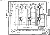
- the constitutions of electric circuits of the inverter circuit 140 and the inverter circuit 142 are explained in conjunction with Fig. 2 .
- the inverter circuit 140 and the inverter circuit 142 are extremely similar to each other with respect to the circuit constitution and the manner of operation and hence, the explanation is made hereinafter by taking the inverter circuit 140 as a representing example. Further, in the explanation made hereinafter, an insulated-gate bipolar transistor is used as a semiconductor element, and the insulated-gate bipolar transistor is abbreviated as IGBT hereinafter.
- a series circuit of upper and lower arms 150 is constituted of an IGBT 328 and a diode 156 which are operated as an upper arm and an IGBT 330 and a diode 166 which are operated as a lower arm.
- the inverter circuit 140 includes these series circuits of upper and lower arms 150 corresponding to three phases, that is, a U phase, a V phase and a W phase of AC power to be outputted.
- these three phases respectively correspond to respective windings of three phases of armature winding of the motor generator MG1.
- an AC current is outputted from an intermediate electrode 169 which is a middle portion of the series circuit.
- the intermediate electrode 169 is connected to AC bus bars 802, 804 via the AC terminal 159 and the AC terminal 188, wherein the AC terminal 159 and the AC terminal 188 are AC power lines leading to the motor generator MG1, and are explained hereinafter.
- a collector electrode 153 of the IGBT 328 of the upper arm is electrically connected to a positive-pole-side capacitor terminal 506 of the capacitor module 500 via a positive pole terminal 157.
- An emitter electrode of the IGBT 330 of the lower arm is electrically connected to a negative-pole-side capacitor terminal 504 of the capacitor module 500 via a negative pole terminal 158.
- control circuit 172 receives control commands from the host control device via the connector 31; generates control pulses which are control signals for controlling the IGBTs 328 and the IGBTs 330 which constitute the upper arms or the lower arms of the series circuits of upper and lower arms 150 of respective phases which form the inverter circuit 140 based on the control commands; and supplies the control pulses to the driver circuit 174.
- the driver circuit 174 supplies drive pulses for controlling the IGBTs 328 or the IGBTs 330 which constitute the upper arms or the lower arms of the series circuit of upper and lower arms 150 of respective phases based on the above-mentioned control pulse.
- the IGBTs 328 and the IGBTs 330 perform a conduction operation or an interruption operation based on the drive pulses from the driver circuit 174 thus converting DC power supplied from the battery 136 into three-phase AC power.
- the converted power is supplied to the motor generator MG1.
- the IGBT 328 includes the collector electrode 153, an emitter electrode 155 for signal, and a gate electrode 154.
- the IGBT 330 includes a collector electrode 163, an emitter electrode 165 for signal, and a gate electrode 164.
- the diode 156 is electrically connected between the collector electrode 153 and the emitter electrode 155.
- the diode 166 is electrically connected between the collector electrode 163 and the emitter electrode 165.
- a metal oxide semiconductor field effect transistor (abbreviated as MOSFET hereinafter) may be used as a switching power semiconductor element.
- MOSFET metal oxide semiconductor field effect transistor
- the diode 156 and the diode 166 become unnecessary.
- an IGBT is suitable for a case where a DC voltage is relatively high
- a MOSFET is suitable for a case where a DC voltage is relatively low.
- the capacitor module 500 includes: the plurality of positive-pole-side capacitor terminals 506; the plurality of negative-pole-side capacitor terminals 504; a positive-pole-side power source terminal 509 and a negative-pole-side power source terminal 508.
- DC power of high voltage from the battery 136 is supplied to the positive-pole-side power source terminal 509 and the negative-pole-side power source terminal 508 via the DC connector 138, and is supplied to the inverter circuit 140 from the positive-pole-side capacitor terminal 506 and the negative-pole-side capacitor terminal 504 of the capacitor module 500.
- DC power which is obtained by the conversion of AC power into DC power by the inverter circuit 140 or the inverter circuit 142 is supplied to the capacitor module 500 from the positive-pole-side capacitor terminal 506 and the negative-pole-side capacitor terminal 504, is supplied to the battery 136 from the positive-pole-side power source terminal 509 and the negative-pole-side power source terminal 508 via the DC connector 138, and is stored in the battery 136.
- the control circuit 172 includes a microcomputer (hereinafter referred to as "micon") for arithmetically processing switching timings of the IGBT 328 and the IGBT 330.
- a target torque value which the motor generator MG1 is required to generate As input information to be inputted to the micon, a target torque value which the motor generator MG1 is required to generate, a current value of an electric current supplied to the motor generator MG1 from the series circuit of upper and lower arms 150, and a magnetic pole position of a rotor of the motor generator MG1 are named.
- a target torque value is based on a command signal outputted from a host control device not shown in the drawing.
- a current value is detected based on a detection signal transmitted from a current sensor 180.
- a magnetic pole position is detected based on a detection signal outputted from a rotation magnetic pole sensor (not shown in the drawing) such as a resolver mounted on the motor generator MG1.
- a rotation magnetic pole sensor such as a resolver mounted on the motor generator MG1.
- the micon in the control circuit 172 calculates current command values on a d axis and a q axis of the motor generator MG1 based on a target torque value, calculates voltage command values on the d axis and the q axis based on the difference between the calculated current command values on the d axis and the q axis and the detected current values on the d axis and the q axis, and converts the calculated voltage command values on the d axis and the q axis into voltage command values of a U phase, a V phase and a W phase based on detected magnetic pole positions.
- the micon generates a pulse-shaped modulated wave based on a comparison between a fundamental wave (sinusoidal wave) based on the voltage command values of the U phase, the V phase and the W phase and a carrier wave (triangular wave), and outputs the generated modulated wave to the driver circuit 174 as a PWM (pulse width modulation) signal.
- a fundamental wave sinusoidal wave
- a carrier wave triangular wave
- the driver circuit 174 in driving the lower arm, outputs a drive signal obtained by amplifying the PWM signal to a gate electrode of the IGBT 330 of the corresponding lower arm.
- the driver circuit 174 in driving the upper arm, amplifies a PWM signal after shifting a level of a reference potential of the PWM signal to a level of a reference potential of the upper arm, and outputs the amplified PWM signal to a gate electrode of the IGBT 328 of the corresponding upper arm as a drive signal.
- the micon in the control circuit 172 performs the detection of abnormality (an overcurrent, an overvoltage, an overtemperature or the like) thus protecting the series circuit of upper and lower arms 150. Accordingly, sensing information is inputted to the control circuit 172. For example, information on electric currents which are supplied to an emitter electrode of the IGBT 328 and an emitter electrode of the IGBT 330 is respectively inputted to a corresponding drive part (IC) from the emitter electrode 155 for signal and the emitter electrode 165 for signal of the respective arms.
- IC drive part
- each drive part (IC) performs the overcurrent detection, and stops a switching operation of the corresponding IGBT 328 or IGBT 330 when an overcurrent is detected thus protecting the corresponding IGBT 328 or IGBT 330 from an overcurrent.
- Information on the temperature of the series circuit of upper and lower arms 150 is inputted to the micon from a temperature sensor (not shown in the drawing) mounted in the series circuit of upper and lower arms 150. Further, information on a voltage on a DC positive pole side of the series circuit of upper and lower arms 150 is inputted in the micon. The micon performs the overtemperature detection and the overvoltage detection based on these information, and stops the switching operations of all IGBTs 328 and IGBTs 330 when an overtemperature or an overvoltage is detected.
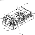
- Fig. 3 to Fig. 5 are views showing the schematic constitution of the power conversion device 200 according to this embodiment, wherein Fig. 3 is a perspective view of the power conversion device 200, Fig. 4 is an exploded perspective view of the power conversion device 200, and Fig. 5 is a cross-sectional view taken along a line A-A in Fig. 3 .
- a shape of the power conversion device 200 as viewed in a plan view is formed into an approximately rectangular shape so that the power conversion device 200 can acquire advantageous effects that the power conversion device 200 can be easily mounted on a vehicle, and can be easily manufactured.
- the power conversion device 200 includes a housing and a lid made of aluminum which are fixed to the transmission TM, and circuit parts of the power conversion device 200 are housed in the inside of the housing. However, in Fig. 3 to Fig. 5 , the illustration of the housing and the lid is omitted.
- the power conversion device 200 includes: a cooling base 5 in which the capacitor module 500 and a power modules 1 are housed; and a drive circuit board 2, a control circuit board 3 and the like which are arranged over the cooling base 5.
- the above-mentioned control circuit 172 is mounted on the control circuit board 3.
- a flow passage 51 through which a cooling medium flows, and a capacitor housing portion 54 which is formed such that the capacitor housing portion 54 is surrounded by the flow passage 51 are formed.
- the capacitor module 500 is housed in the capacitor housing portion 54, and is cooled through a wall surface of the flow passage 51.
- a plurality of opening portions 50 are formed in the cooling base 5 along the flow passage 51.
- the power module 1 is constituted such that the above-mentioned series circuit of upper and lower arms 150 is housed in the inside of a metal casing, and generates the largest heat value among the electronic parts. Accordingly, the plurality of power modules 1 are inserted into the inside of the flow passage 51 through the opening portions 50 and are directly cooled by a cooling medium.
- An inlet port 13IN and a discharge port 14OUT are formed in a bottom portion of the cooling base 5.
- a cooling medium for example, cooling water flows into the inside of the flow passage 51 through the inlet port 13IN, circulates in the flow passage 51 and, thereafter, is flown out from the discharge port 14OUT.
- the control circuit board 3 is arranged on an upper portion of a board base 7 made of aluminum which is fixed to support struts of the cooling base 5, and the drive circuit board 2 is arranged on a lower side of the board base 7.
- the drive circuit board 2 and the control circuit board 3 are thermally connected to the board base 7 made of aluminum so that heat generated in the drive circuit board 2 and the control circuit board 3 is leaked to a cooling medium in the flow passage 51 from the board base 7 through support struts 55.
- the board base 7 also functions as an electromagnetic shield for a group of circuits mounted on the drive circuit board 2 and the control circuit board 3.
- the connector 31 is mounted on the control circuit board 3.
- the connector 31 is connected with an external control device, and the signal transmission is performed between the control circuit 172 mounted on the control circuit board 2 and the external control device such as a host control device.
- DC power of a low voltage for operating the control circuits in the inside of the power conversion device 200 is supplied from the connector 31.
- the direction of a fitting surface of a terminal such as the connector 31 differs variously depending on a type of a vehicle, particularly in a case of mounting the power conversion device 200 on a small-sized vehicle, it is preferable to arrange the terminal such that the fitting surface is exposed upwardly from a viewpoint of the restriction imposed due to a size of the inside of an engine room or assembling property.
- the power conversion device 200 is arranged above a transmission TM, the operability is enhanced by projecting the fitting surface of the terminal toward a side opposite to a side where the transmission TM is arranged.
- Fig. 6 is an exploded perspective view of the cooling base 5, and is a view of the cooling base as viewed from a bottom surface side.
- the flow passage 51 is formed such that the flow passage 51 surrounds the capacitor housing portion 54.
- One end of the flow passage 51 is communicated with the inlet port 13IN formed in a lower cover 420, and the other end of the flow passage 51 is communicated with the discharge port 14OUT formed in the lower cover 420.
- projecting portions 406 are formed on the lower cover 420 at positions where the openings 50 face the flow passage 51 respectively.
- Distal end portions of the power modules 1 which are inserted into the flow passage 51 are inserted into the inside of recessed portions formed in the projecting portions 406.
- Numeral 409 indicates a seal member for sealing a gap formed between the lower cover 420 and the cooling base 5.
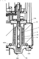
- Fig. 7 is a view showing a part of the cross-sectional view shown in Fig. 4 in such a manner that a portion of the flow passage portion in which the power modules 1 are housed is shown in an enlarged manner.
- An opening of the flow passage 51 which is formed in the cooling base 5 on a base back surface side is hermetically closed by the lower cover 420.
- a cylindrical portion on which radiator fins 14 are formed is inserted into the flow passage 51 through the opening portion 50 (see Fig. 5 ) and a flange portion 13b is fixed to an upper surface of the cooling base 5.
- a distal end portion (lower end portion in the drawing) of a cylindrical portion 13a of the power module 1 is inserted into the recessed portion formed in the projecting portion 406 of the lower cover 420.
- a seal member 16 is provided to a sealing portion between the flange portion 13b and the cooling base 5, and the opening portion 50 is hermetically sealed by the flange portion 13b. Apart of the seal member 16 is inserted into a gap formed between the flange portion 13b and the radiator fins 14.
- Fig. 8 is a cross-sectional view of the power module 1
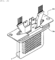
- Fig. 9 is a perspective view of the external appearance of the power module 1.
- the power module 1 is constituted such that the power semiconductor element (IGBT 9 and diode 10) which constitutes the above-mentioned series circuit of upper and lower arms 150 is incorporated in a can-shaped casing 13 made of aluminum.
- the IGBT 9 corresponds to IGBTs 154, 164 in Fig. 2 and the diode 10 corresponds to the diodes 156, 166 in Fig. 2 .
- the casing 13 includes the cylindrical portion 13a in which a transfer mold body is housed, and the flange portion 13b for fixing the power module 1 to the cooling base 5. As shown in Fig.
- the IGBT 9 and the diode 10 which are incorporated in the cylindrical portion 13a have both front and back surfaces thereof sandwiched by copper leads 11 which constitute electrodes respectively, and these parts are formed into an integral body by transfer molding using a resin 12. Terminal portions 11b of the copper leads 11 project toward the outside of the casing 13 from the flange portion 13b.
- the casing 13 plays a role of a radiator which radiates heat generated from the power semiconductor element.
- the casing 13 is constituted such that the plurality of radiator fins (pin fins) 14 are mounted in a raised manner on outer peripheral surfaces of thick wall portions 130 of the cylindrical portion 13a, that is, on radiation surfaces.
- the periphery of the thick wall portion 130 forms a thin wall portion 131.
- a transfer mold body is inserted into the inside of the casing 13 in a state where the transfer mold body is sandwiched by insulation sheets having an adhesive property.
- a back surface side of the copper leads 11 is exposed on both front and back surfaces of the transfer mold body, and the thick wall portions 130 are pressed toward the inside of the casing such that the exposed surfaces are brought into close contact with an inner peripheral surface of the casing 13 with the above-mentioned insulation sheet sandwiched therebetween.
- the thin wall portions 131 are plastically deformed, and inner peripheral surfaces of the thick wall portions 130 are brought into close contact with and are fixed to both front and back surfaces of the transfer mold body.
- the casing 13 is, for reducing a manufacturing cost, formed of an integral-body-type vessel which is formed in such a manner that the forming of the casing 13 into a can shape, the forming of the radiator fins 14, and the forming of the flange portion 13b are performed by forging.
- a gap of approximately 5 to 10 mm is formed between the flange portion 13b and the radiator fins 14.
- the radiator fins 14 and the flange portion 13b may be formed by cutting. Also in this case, a gap into which a tool enters is necessary at the time of cutting a sealing surface of the flange portion 13b and hence, a gap is formed between the flange portion 13b and the radiator fins 14.
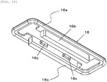
- Fig. 10 is a perspective view showing a shape of the seal member 16.
- the seal member 16 includes an O-ring portion 16a having the approximately rectangular annular structure, and a pair of flow passage control portions 16b which are integrally formed inside the O-ring portion 16a.
- the pair of flow passage control portions 16b are formed along a long side of the O-ring portion 16a, and projections 16c are formed on surfaces of the flow passage control portions 16b which face each other in an opposed manner respectively.
- the projections 16c are brought into contact with the thin wall portions 131 formed between the flange portion 13b and the thick wall portions 130.
- Fig. 11 is a plan view showing the opening portion 50 of the cooling base 5.
- a seal groove 52 is formed around the approximately rectangular opening portion 50.
- the O-ring portion 16a of the seal member 16 is placed on an upper surface of the seal groove 52 as indicated by a double-dashed chained line.
- the flow passage control portions 16b which are formed on a lower surface side (on a back surface side of the paper that the drawing is on) of the seal member 16 are arranged in the inside of the flow passage 51.
- Numeral 53 indicates threaded holes for fixing the flange portion 13b of the power module 1 to the opening portion 50 of the cooling base 5 by bolts.
- a broken line 51a indicates a flow passage between the opening portions 50.
- the seal member 16 is mounted on the power module 1 from a lower end of the cylindrical portion 13a as indicated by an arrow thus arranging the seal member 16 on a back surface side (sealing surface side) of the flange portion 13b. Thereafter, the cylindrical portion 13a of the power module 1 is inserted into the inside of the opening portion 50, and the flange portion 13b is placed on the cooling base 5 such that the O-ring portion 16a of the seal member 16 is arranged in the seal groove 52.
- a pusher plate 17 having the approximately same outer peripheral shape as the flange portion 13b is arranged on the flange portion 13b, and the pusher plate 17 and the flange portion 13b are fastened together to the cooling base 5 using bolts 18.
- the pusher plate 17 it is possible to prevent the flange portion 13b made of aluminum from being deformed at the time of fastening the flange portion 13b by bolts so that uniform sealing can be acquired.
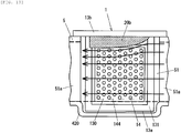
- Fig. 12 and Fig. 13 are views for explaining the manner of operation of the flow passage control portion 16b.
- Fig. 12 shows a case where the flow passage control portions 16b are formed in the power module 1
- Fig. 13 shows a case where the flow passage control portion 16b is not formed in the power module 1.
- (a) is a cross-sectional view taken along a line orthogonal to the flow of a cooling medium
- (b) is a cross-sectional view taken along a line along the flow of the cooling medium.
- a region surrounded by a double-dashed chained line 144 in Fig. 12 and Fig. 13 is a region where the plurality of radiator fins 14 are formed.
- the double-dashed chained line 144 indicates a group of radiator fins.
- a recessed portion is formed on the lower cover 420 which constitutes a bottom surface of the flow passage 51 in a state where the recessed portion conforms to a bottom surface of the power module 1 in shape thus preventing the formation of a space on a bottom surface side through which a cooling medium bypasses.
- Fig. 13(a) which is the cross-sectional view
- a gap of a predetermined distance D is formed between the flange portion 13b of the power module 1 and the group of radiator fins 144. This is an unavoidable gap due to the restriction imposed from a viewpoint of manufacture as described previously, and the predetermined distance D becomes approximately 5 mm to 10 mm when the casing 13 is formed by forging.
- the cooling medium flows into the flow passage 51 into which the power module 1 is inserted. While most of the flown cooling medium flows toward a left side in the drawing in such a manner that the cooling medium passes through the gaps formed between the radiator fins 14, some cooling medium flows through a region 51c where the radiator fins 14 are not formed in a bypassed manner as indicated by a stream line 511. As a result, a flow rate of the cooling medium which passes through the portion where the radiator fins 14 are formed is decreased resulting in the lowering of cooling ability of the power module 1.
- the cooling medium enters the region 51c by going around the blocking member on a downstream side of the blocking member. Further, a vortex is generated behind the blocking member or the like so that a pressure loss is increased. Accordingly, as shown in Fig. 12(b) , it is preferable that the flow passage control portion 16b is continuously arranged in the gap regions 51c having a length corresponding to a width of the group of radiator fins 144 along the flow direction of the cooling medium in the inside of the gap region 51c.
- the flow passage control portion 16b is integrally formed with the O-ring portion 16a of the flange portion 13b, the number of man-hours of an assembling operation can be reduced, and the constitution is also useful for preventing a person from forgetting the assembling of the flow passage control portion 16b.
- the flow passage control portion 16b occupies the whole space between the flange portion 13b and the group of radiator fins 144.
- the radiator fin 14 is formed of a pin fin, it is preferable to set the distance between the pins to approximately 2 to 3 mm.
- Fig. 14 is a view showing a modification of the above-mentioned seal member 16.
- a seal member 20 shown in Fig. 14 also is formed of an O-ring portion 20a and flow passage control portions 20b.
- the O-ring portion 20a has the same shape as the O-ring portion 16a shown in Fig. 10 .
- the shape of the flow passage control portion 20b differs from the shape of the flow passage control portion 16b. That is, the flow passage control portion 20b has a shape where a height H of the flow passage control portion 20b is increased gradually in the leftward direction in the drawing.
- the seal member 20 is mounted in such a manner that a side of the seal member 20 where the flow passage control portion 20b has a larger height H is positioned on a more downstream side of the cooling medium.
- a distance between the flow passage control portion 20b and the group of radiator fins 144 is gradually decreased along the flow of the cooling medium and hence, as indicated by a stream line, a cooling medium flows toward the group of radiator fins 144 along an inclined bottom surface of the flow passage control portion 20b.
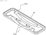
- the shape of the above-mentioned flow passage control portion 20b may be deformed into a shape of a flow passage control portion 21b shown in Fig. 16 .
- an inclined bottom surface is formed on both of an upstream side and a downstream side of the flow of a cooling medium. That is, the flow passage control portion 21b is formed into a shape where a distance between the flow passage control portion 21b and the group of radiator fins 144 becomes minimum at the center of the group of radiator fins 144 in the flow direction, and the distance is gradually increased in terms of being further away from the center of the group of radiator fins 144.
- a quantity of cooling medium which does not pass through the radiator fins 14 can be reduced so that a flow speed of the cooling medium which hits the radiator fins 14 can be increased and hence, the cooling ability of the power module 1 can be enhanced.
- the enhancement of the cooling ability contributes to the miniaturization of the cooling device and the power module.
- the power module 1 is allowed to generate a large quantity of heat value and hence, a size of a power-supply-use power semiconductor can be decreased thus contributing to the reduction of cost.
- the flow passage control portions 20b, 21b having a shape shown in Fig. 14 and Fig. 16 .
- the flow passage control portions 16b shown in Fig. 10 which has the structure where a cooling medium does not go around between the flange portion 13b and the group of radiator fins 144.
- the present invention can cope with a plurality of vehicles having different specifications on requirements using the same power module 1 and hence, the power conversion device of the same type can cope with a plurality of vehicles whereby a development cost and a manufacturing cost can be lowered.
- the O-ring portion of the flange portion 13b which has a sealing function, and the flow passage control portion which blocks the flow of a cooling medium are integrally formed.
- the O-ring portion may be formed as a body separate from the flow passage control portion.
- a standard seal material is used as a seal member 22 of the flange portion 13b.
- Two independent flow passage control members 23 are arranged between the flange portion 13b and the radiator fins 14.
- the flow passage control member 23 shown in Fig. 17 has the substantially same shape as the flow passage control portion 16b shown in Fig. 10 .
- a seal member having a standard shape is used as the seal member 22 and hence, it is unnecessary to particularly prepare a dedicated mold so that a manufacturing cost of the seal member can be suppressed.
- the pusher plate 17 is used for fixing the power module 1.
- the casing 13 is formed using an extremely soft pure-aluminum-based material by forging and hence, when the flange portion 13b is fixed by bolts without using the pusher plate 17, the flange portion 13b is deformed due to a repulsive force of the seal member 16.
- the pusher plate 17 is formed using a material such as steel.
- the bolt holes 13c through which the bolt passes are formed also in the flange portion 13b of the casing 13 thus adopting the configuration where the pusher plate 17 and the flange portion 13b are fastened together. Further, as shown in Fig. 9 and Fig.
- the arrangement of the power modules 1 can be changed depending on restriction conditions imposed on a shape of the whole power conversion device and hence, when a pusher plate is used, it is desirable to cope with the change in the arrangement of the power modules 1 by only changing of the pusher plate without forming bolt holes for fixing by bolts in the power modules 1 even when the arrangement of the power modules 1 is changed.
- Fig. 18 shows one example of the constitution where bolt holes are not formed in the flange portion 13b.
- the bolt holes for fixing by bolts are not formed in the flange portion 13b of the power module 1 and hence, a pusher plate 24 is directly fixed to the cooling base 5 by bolts in place of being fastened together with the flange portion 13b. Accordingly, to absorb the manufacture tolerances of thicknesses of the flange portion 13b and a seal member, a shape of the pusher plate 24 in the vicinity of the bolt hole is formed into a zigzag spring shape.
- one pusher plate 24 is necessary for every power module.
- three power modules 1 are fixed using one pusher plate 25 and hence, the number of bolts can be decreased whereby the number of man-hours in assembling can be decreased.
- the radiator fins 14 are formed of a pin fin.
- the radiator fins 14 may have other shapes and, for example, the radiator fins may be formed of a straight fin.
- the above-mentioned casing 13 is integrally formed by forging, even in a case of a cylindrical casing which is formed by other manufacturing methods, the formation of a gap between the flange portion 13b for fixing the power module 1 to the cooling base 5 and the group of radiator fins 144 is unavoidable in terms of manufacture. Accordingly, by arranging a flow passage control portion in such a gap, the substantially same advantageous effects as the above-mentioned embodiment can be obtained. Particularly, in the case of the casing shown in Fig.
- the thin wall portion 131 for plastic deformation is formed between the flange portion 13b and the group of radiator fins 144 and hence, it is impossible to prevent the further increase of the gap between the flange portion 13b and the group of the radiator fins 144 whereby advantageous effects brought about by the provision of the flow passage control portion is further increased.
- the explanation has been made by taking the vehicle-mounted power conversion device mounted on an electric vehicle or a hybrid vehicle as an example.
- the power conversion device is a power conversion device having the cooling structure where a power module is immersed in a cooling medium
- the present invention is also applicable to such a power conversion without departing from the scope of the attached claims.
Landscapes
- Engineering & Computer Science (AREA)
- Power Engineering (AREA)
- Physics & Mathematics (AREA)
- Thermal Sciences (AREA)
- Microelectronics & Electronic Packaging (AREA)
- Inverter Devices (AREA)
- Cooling Or The Like Of Semiconductors Or Solid State Devices (AREA)
Claims (6)
- Leistungsumsetzungsvorrichtung (200), die Folgendes umfasst:ein Strömungskanalgehäuse (13), in dem ein Strömungskanal (51) gebildet ist, durch den ein Kühlmedium strömt, und ein Öffnungsabschnitt (50) gebildet ist, der mit dem Strömungskanal in Verbindung steht;ein Leistungsmodul (1), das einen zylindrischen Grundabschnitt (13a), in dem ein Leistungshalbleiterelement aufgenommen ist und der durch den Öffnungsabschnitt in den Strömungskanal eingeführt ist, einen Flanschabschnitt (13b), der auf einer Öffnung des zylindrischen Abschnitts gebildet ist und am Strömungskanalgehäuse arretiert ist, um den Öffnungsabschnitt zu verschließen, und eine erste Gruppe Kühlerrippen (14, 144), die auf einer Außenumfangsfläche des zylindrischen Abschnitts angebracht sind, wobei ein Spalt mit einem vorgegebenen Abstand zwischen dem Flanschabschnitt und der ersten Gruppe Kühlerrippen gebildet ist, aufweist; undeine zweite Gruppe Kühlerrippen (14, 144), die auf einer Außenumfangsfläche des zylindrischen Abschnitts angebracht sind, wobei ein Spalt mit einem vorgegebenen Abstand zwischen dem Flanschabschnitt und der zweiten Gruppe Kühlerrippen gebildet ist;gekennzeichnet durchein erstes Strömungskanal-Steuerelement (16b, 20b), das in dem Spalt angeordnet ist, der zwischen dem Flanschabschnitt und der ersten Gruppe Kühlerrippen gebildet ist, und das Kühlmedium in die erste Gruppe Kühlerrippen einbringt;ein zweites Strömungskanal-Steuerelement (16b, 20b), das gegenüber dem ersten Strömungskanal-Steuerelement angeordnet ist, wobei der zylindrische Grundabschnitt dazwischen eingebettet ist, und das Kühlmedium in die zweite Gruppe Kühlerrippen einbringt; undein Dichtungselement (20), das einen Ringabschnitt aufweist, der das erste Strömungskanal-Steuerelement und das zweite Strömungskanal-Steuerelement verbindet;wobei das Dichtungselement auf dem zylindrischen Grundabschnitt angebracht ist; undwobeidurch einen Schaltvorgang des Leistungshableiterelements Leistung von Gleichstromleistung in Wechselstromleistung oder von Wechselstromleistung in Gleichstromleistung umgesetzt wird.
- Leistungsumsetzungsvorrichtung nach Anspruch 1, wobei das erste Strömungskanal-Steuerelement derart angeordnet ist, dass ein minimaler Abstand zwischen dem ersten Strömungskanal-Steuerelement und der ersten Gruppe Kühlerrippen kleiner oder gleich einem Abstand zwischen den Rippen der Gruppe Kühlerrippen eingestellt ist, und
wobei das zweite Strömungskanal-Steuerelement derart angeordnet ist, dass ein minimaler Abstand zwischen dem zweiten Strömungskanal-Steuerelement und der zweiten Gruppe Kühlerrippen kleiner oder gleich einem Abstand zwischen den Rippen der zweiten Gruppe Kühlerrippen eingestellt ist. - Leistungsumsetzungsvorrichtung nach Anspruch 1, wobei das erste Strömungskanal-Steuerelement auf ununterbrochene Weise entlang der Strömungsrichtung des Kühlmediums in dem Spalt verteilt ist, und
wobei das zweite Strömungskanal-Steuerelement auf ununterbrochene Weise entlang der Strömungsrichtung des Kühlmediums in dem Spalt verteilt ist. - Leistungsumsetzungsvorrichtung nach Anspruch 3, wobei das erste Strömungskanal-Steuerelement eine Form aufweist, durch die der Abstand zwischen dem ersten Strömungskanal-Steuerelement und der ersten Gruppe Kühlerrippen entlang der Strömungsrichtung des Kühlmediums verkleinert wird, und
wobei das zweite Strömungskanal-Steuerelement eine Form aufweist, durch die der Abstand zwischen dem zweiten Strömungskanal-Steuerelement und der zweiten Gruppe Kühlerrippen entlang der Strömungsrichtung des Kühlmediums verkleinert wird. - Leistungsumsetzungsvorrichtung nach Anspruch 3, wobei das erste Strömungskanal-Steuerelement eine Form aufweist, durch die der Abstand zwischen dem ersten Strömungskanal-Steuerelement und der ersten Gruppe Kühlerrippen in der Strömungsrichtung in der Mitte der ersten Gruppe Kühlerrippen minimal wird und der Abstand mit zunehmender Entfernung von der Mitte in der Strömungsrichtung allmählich vergrößert wird, und
wobei das zweite Strömungskanal-Steuerelement eine Form aufweist, durch die der Abstand zwischen dem zweiten Strömungskanal-Steuerelement und der zweiten Gruppe Kühlerrippen in der Strömungsrichtung in der Mitte der zweiten Gruppe Kühlerrippen minimal wird und der Abstand mit zunehmender Entfernung von der Mitte in der Strömungsrichtung allmählich vergrößert wird. - Leistungsumsetzungsvorrichtung nach Anspruch 1, wobei das erste Strömungskanal-Steuerelement mit dem Dichtungselement, das zwischen dem Strömungskanalgehäuse und dem Flanschabschnitt angeordnet ist, einteilig ausgebildet ist und
wobei das zweite Strömungskanal-Steuerelement mit dem Dichtungselement, das zwischen dem Strömungskanalgehäuse und dem Flanschabschnitt angeordnet ist, einteilig ausgebildet ist.
Applications Claiming Priority (2)
| Application Number | Priority Date | Filing Date | Title |
|---|---|---|---|
| JP2010168813A JP5439309B2 (ja) | 2010-07-28 | 2010-07-28 | 電力変換装置 |
| PCT/JP2011/066853 WO2012014842A1 (ja) | 2010-07-28 | 2011-07-25 | 電力変換装置 |
Publications (3)
| Publication Number | Publication Date |
|---|---|
| EP2600516A1 EP2600516A1 (de) | 2013-06-05 |
| EP2600516A4 EP2600516A4 (de) | 2018-01-24 |
| EP2600516B1 true EP2600516B1 (de) | 2020-09-30 |
Family
ID=45530050
Family Applications (1)
| Application Number | Title | Priority Date | Filing Date |
|---|---|---|---|
| EP11812431.2A Active EP2600516B1 (de) | 2010-07-28 | 2011-07-25 | Stromwandler |
Country Status (5)
| Country | Link |
|---|---|
| US (1) | US9078376B2 (de) |
| EP (1) | EP2600516B1 (de) |
| JP (1) | JP5439309B2 (de) |
| CN (1) | CN103026605B (de) |
| WO (1) | WO2012014842A1 (de) |
Families Citing this family (28)
| Publication number | Priority date | Publication date | Assignee | Title |
|---|---|---|---|---|
| JP5370448B2 (ja) * | 2011-09-19 | 2013-12-18 | 株式会社デンソー | 電力変換装置 |
| JP5949286B2 (ja) * | 2012-07-31 | 2016-07-06 | 株式会社デンソー | 電力変換装置 |
| JP2014072395A (ja) | 2012-09-28 | 2014-04-21 | Toyota Industries Corp | 冷却装置 |
| JP6262422B2 (ja) | 2012-10-02 | 2018-01-17 | 昭和電工株式会社 | 冷却装置および半導体装置 |
| US9204573B2 (en) * | 2013-05-08 | 2015-12-01 | Kabushiki Kaisha Toshiba | Power conversion apparatus |
| JP6101609B2 (ja) * | 2013-09-20 | 2017-03-22 | 日立オートモティブシステムズ株式会社 | パワー半導体モジュール及びそれを用いた電力変換装置 |
| US9992915B2 (en) | 2013-10-07 | 2018-06-05 | Hitachi Automotive Systems, Ltd. | Power conversion device |
| US20150138734A1 (en) * | 2013-11-18 | 2015-05-21 | Magna Electronics Inc. | 360 degree direct cooled power module |
| JP6193173B2 (ja) * | 2014-04-17 | 2017-09-06 | 日立オートモティブシステムズ株式会社 | 電力変換装置 |
| WO2015198411A1 (ja) * | 2014-06-25 | 2015-12-30 | 株式会社日立製作所 | パワーモジュール装置、電力変換装置およびパワーモジュール装置の製造方法 |
| DE112015002587B4 (de) * | 2014-06-26 | 2021-04-15 | Hitachi Automotive Systems, Ltd. | Leistungshalbleitermodul und herstellungsverfahren des leistungshalbleitermoduls |
| JP6302803B2 (ja) * | 2014-09-09 | 2018-03-28 | 日立オートモティブシステムズ株式会社 | パワー半導体モジュール及びその製造方法、電力変換装置 |
| US10037952B2 (en) * | 2015-02-10 | 2018-07-31 | Mediatek Inc. | Integrated circuit, electronic device and method for transmitting data in electronic device |
| US9978692B2 (en) * | 2015-02-10 | 2018-05-22 | Mediatek Inc. | Integrated circuit, electronic device and method for transmitting data in electronic device |
| WO2017033295A1 (ja) * | 2015-08-26 | 2017-03-02 | 日立オートモティブシステムズ株式会社 | 構造体 |
| JP6593221B2 (ja) * | 2016-02-23 | 2019-10-23 | 株式会社デンソー | 電力変換装置 |
| WO2017149801A1 (ja) * | 2016-03-02 | 2017-09-08 | 三菱電機株式会社 | 電力変換装置 |
| WO2017187781A1 (ja) * | 2016-04-28 | 2017-11-02 | 日立オートモティブシステムズ株式会社 | 電力変換装置 |
| JP7264159B2 (ja) * | 2018-04-06 | 2023-04-25 | ニデック株式会社 | 電力変換装置 |
| JP7159620B2 (ja) * | 2018-05-30 | 2022-10-25 | 富士電機株式会社 | 半導体装置、冷却モジュール、電力変換装置及び電動車両 |
| JP7208757B2 (ja) * | 2018-10-03 | 2023-01-19 | 川崎重工業株式会社 | 制御装置 |
| JP7233014B2 (ja) * | 2018-12-26 | 2023-03-06 | パナソニックIpマネジメント株式会社 | 電力変換装置 |
| JP6777203B2 (ja) * | 2019-08-09 | 2020-10-28 | 株式会社デンソー | 電力変換装置 |
| JP2022188312A (ja) * | 2019-11-27 | 2022-12-21 | 日立Astemo株式会社 | パワーモジュールおよびパワーモジュールの製造方法 |
| JP7419050B2 (ja) | 2019-12-16 | 2024-01-22 | 日立Astemo株式会社 | パワーモジュール、電力変換装置、およびパワーモジュールの製造方法 |
| JP7294455B2 (ja) * | 2019-12-19 | 2023-06-20 | 東芝三菱電機産業システム株式会社 | 電力変換装置およびその製造方法 |
| KR102810533B1 (ko) * | 2020-02-28 | 2025-05-22 | 현대모비스 주식회사 | 전력변환장치의 냉각구조체 |
| CN112053999B (zh) * | 2020-08-10 | 2022-05-13 | 浙江艾罗网络能源技术股份有限公司 | 一种用于固定逆变器晶体管的高强度绝缘压块 |
Family Cites Families (9)
| Publication number | Priority date | Publication date | Assignee | Title |
|---|---|---|---|---|
| JPH02210899A (ja) * | 1989-02-09 | 1990-08-22 | Fujitsu Ltd | 印刷配線板ユニットの冷却構造 |
| DE19643717A1 (de) * | 1996-10-23 | 1998-04-30 | Asea Brown Boveri | Flüssigkeits-Kühlvorrichtung für ein Hochleistungshalbleitermodul |
| JP4168825B2 (ja) | 2003-05-07 | 2008-10-22 | トヨタ自動車株式会社 | 半導体モジュールおよび半導体モジュールを搭載した半導体モジュールユニット |
| US6992382B2 (en) * | 2003-12-29 | 2006-01-31 | Intel Corporation | Integrated micro channels and manifold/plenum using separate silicon or low-cost polycrystalline silicon |
| JP2005348533A (ja) * | 2004-06-03 | 2005-12-15 | Fuji Electric Fa Components & Systems Co Ltd | インバータ装置 |
| JP5120605B2 (ja) * | 2007-05-22 | 2013-01-16 | アイシン・エィ・ダブリュ株式会社 | 半導体モジュール及びインバータ装置 |
| TWI423403B (zh) * | 2007-09-17 | 2014-01-11 | 萬國商業機器公司 | 積體電路疊層 |
| JP5557441B2 (ja) * | 2008-10-31 | 2014-07-23 | 日立オートモティブシステムズ株式会社 | 電力変換装置および電動車両 |
| US8064198B2 (en) * | 2009-06-29 | 2011-11-22 | Honda Motor Co., Ltd. | Cooling device for semiconductor element module and magnetic part |
-
2010
- 2010-07-28 JP JP2010168813A patent/JP5439309B2/ja active Active
-
2011
- 2011-07-25 EP EP11812431.2A patent/EP2600516B1/de active Active
- 2011-07-25 CN CN201180036876.6A patent/CN103026605B/zh active Active
- 2011-07-25 WO PCT/JP2011/066853 patent/WO2012014842A1/ja not_active Ceased
- 2011-07-25 US US13/811,497 patent/US9078376B2/en active Active
Non-Patent Citations (1)
| Title |
|---|
| None * |
Also Published As
| Publication number | Publication date |
|---|---|
| EP2600516A1 (de) | 2013-06-05 |
| CN103026605A (zh) | 2013-04-03 |
| EP2600516A4 (de) | 2018-01-24 |
| JP2012029539A (ja) | 2012-02-09 |
| US9078376B2 (en) | 2015-07-07 |
| WO2012014842A1 (ja) | 2012-02-02 |
| JP5439309B2 (ja) | 2014-03-12 |
| US20130128646A1 (en) | 2013-05-23 |
| CN103026605B (zh) | 2015-09-09 |
Similar Documents
| Publication | Publication Date | Title |
|---|---|---|
| US9078376B2 (en) | Power conversion device | |
| JP5851372B2 (ja) | 電力変換装置 | |
| JP5508357B2 (ja) | 電力変換装置 | |
| JP4452953B2 (ja) | 電力変換装置 | |
| US8659130B2 (en) | Power module and power module manufacturing method | |
| US9419535B2 (en) | Electric power converter | |
| US9596782B2 (en) | Power converter with cooling board | |
| JP5815063B2 (ja) | 電力変換装置 | |
| JP5707279B2 (ja) | 電力変換装置 | |
| WO2011162241A1 (ja) | 電力変換装置 | |
| JP2011217550A (ja) | 電力変換装置 | |
| JP2011217548A (ja) | 電力変換装置 | |
| JP2010245910A (ja) | 電力変換装置及びそれを用いた車載用電機システム | |
| CN101946395A (zh) | 功率模块、电力转换装置以及电动车辆 | |
| JP2013005067A (ja) | 電力変換装置 | |
| WO2021225072A1 (ja) | 電力変換装置 | |
| JP2010011671A (ja) | 電力変換装置 | |
| JP5623985B2 (ja) | 電力変換装置 | |
| JP2014166043A (ja) | 電力変換装置 | |
| JP6272064B2 (ja) | 電力変換装置 | |
| JP5798951B2 (ja) | インバータ装置 |
Legal Events
| Date | Code | Title | Description |
|---|---|---|---|
| PUAI | Public reference made under article 153(3) epc to a published international application that has entered the european phase |
Free format text: ORIGINAL CODE: 0009012 |
|
| 17P | Request for examination filed |
Effective date: 20130228 |
|
| AK | Designated contracting states |
Kind code of ref document: A1 Designated state(s): AL AT BE BG CH CY CZ DE DK EE ES FI FR GB GR HR HU IE IS IT LI LT LU LV MC MK MT NL NO PL PT RO RS SE SI SK SM TR |
|
| DAX | Request for extension of the european patent (deleted) | ||
| RA4 | Supplementary search report drawn up and despatched (corrected) |
Effective date: 20180102 |
|
| RIC1 | Information provided on ipc code assigned before grant |
Ipc: H01L 25/07 20060101ALI20171219BHEP Ipc: H01L 23/367 20060101ALI20171219BHEP Ipc: H01L 23/473 20060101ALI20171219BHEP Ipc: H01L 25/18 20060101ALI20171219BHEP Ipc: H02M 7/48 20070101AFI20171219BHEP |
|
| GRAP | Despatch of communication of intention to grant a patent |
Free format text: ORIGINAL CODE: EPIDOSNIGR1 |
|
| STAA | Information on the status of an ep patent application or granted ep patent |
Free format text: STATUS: GRANT OF PATENT IS INTENDED |
|
| INTG | Intention to grant announced |
Effective date: 20200402 |
|
| GRAJ | Information related to disapproval of communication of intention to grant by the applicant or resumption of examination proceedings by the epo deleted |
Free format text: ORIGINAL CODE: EPIDOSDIGR1 |
|
| STAA | Information on the status of an ep patent application or granted ep patent |
Free format text: STATUS: REQUEST FOR EXAMINATION WAS MADE |
|
| GRAP | Despatch of communication of intention to grant a patent |
Free format text: ORIGINAL CODE: EPIDOSNIGR1 |
|
| STAA | Information on the status of an ep patent application or granted ep patent |
Free format text: STATUS: GRANT OF PATENT IS INTENDED |
|
| INTC | Intention to grant announced (deleted) | ||
| INTG | Intention to grant announced |
Effective date: 20200713 |
|
| GRAS | Grant fee paid |
Free format text: ORIGINAL CODE: EPIDOSNIGR3 |
|
| GRAA | (expected) grant |
Free format text: ORIGINAL CODE: 0009210 |
|
| STAA | Information on the status of an ep patent application or granted ep patent |
Free format text: STATUS: THE PATENT HAS BEEN GRANTED |
|
| AK | Designated contracting states |
Kind code of ref document: B1 Designated state(s): AL AT BE BG CH CY CZ DE DK EE ES FI FR GB GR HR HU IE IS IT LI LT LU LV MC MK MT NL NO PL PT RO RS SE SI SK SM TR |
|
| REG | Reference to a national code |
Ref country code: CH Ref legal event code: EP Ref country code: GB Ref legal event code: FG4D |
|
| REG | Reference to a national code |
Ref country code: DE Ref legal event code: R096 Ref document number: 602011068786 Country of ref document: DE Ref country code: AT Ref legal event code: REF Ref document number: 1319834 Country of ref document: AT Kind code of ref document: T Effective date: 20201015 |
|
| REG | Reference to a national code |
Ref country code: IE Ref legal event code: FG4D |
|
| PG25 | Lapsed in a contracting state [announced via postgrant information from national office to epo] |
Ref country code: SE Free format text: LAPSE BECAUSE OF FAILURE TO SUBMIT A TRANSLATION OF THE DESCRIPTION OR TO PAY THE FEE WITHIN THE PRESCRIBED TIME-LIMIT Effective date: 20200930 Ref country code: BG Free format text: LAPSE BECAUSE OF FAILURE TO SUBMIT A TRANSLATION OF THE DESCRIPTION OR TO PAY THE FEE WITHIN THE PRESCRIBED TIME-LIMIT Effective date: 20201230 Ref country code: FI Free format text: LAPSE BECAUSE OF FAILURE TO SUBMIT A TRANSLATION OF THE DESCRIPTION OR TO PAY THE FEE WITHIN THE PRESCRIBED TIME-LIMIT Effective date: 20200930 Ref country code: GR Free format text: LAPSE BECAUSE OF FAILURE TO SUBMIT A TRANSLATION OF THE DESCRIPTION OR TO PAY THE FEE WITHIN THE PRESCRIBED TIME-LIMIT Effective date: 20201231 Ref country code: NO Free format text: LAPSE BECAUSE OF FAILURE TO SUBMIT A TRANSLATION OF THE DESCRIPTION OR TO PAY THE FEE WITHIN THE PRESCRIBED TIME-LIMIT Effective date: 20201230 Ref country code: HR Free format text: LAPSE BECAUSE OF FAILURE TO SUBMIT A TRANSLATION OF THE DESCRIPTION OR TO PAY THE FEE WITHIN THE PRESCRIBED TIME-LIMIT Effective date: 20200930 |
|
| REG | Reference to a national code |
Ref country code: AT Ref legal event code: MK05 Ref document number: 1319834 Country of ref document: AT Kind code of ref document: T Effective date: 20200930 |
|
| PG25 | Lapsed in a contracting state [announced via postgrant information from national office to epo] |
Ref country code: LV Free format text: LAPSE BECAUSE OF FAILURE TO SUBMIT A TRANSLATION OF THE DESCRIPTION OR TO PAY THE FEE WITHIN THE PRESCRIBED TIME-LIMIT Effective date: 20200930 Ref country code: RS Free format text: LAPSE BECAUSE OF FAILURE TO SUBMIT A TRANSLATION OF THE DESCRIPTION OR TO PAY THE FEE WITHIN THE PRESCRIBED TIME-LIMIT Effective date: 20200930 |
|
| REG | Reference to a national code |
Ref country code: NL Ref legal event code: MP Effective date: 20200930 |
|
| REG | Reference to a national code |
Ref country code: DE Ref legal event code: R082 Ref document number: 602011068786 Country of ref document: DE Representative=s name: MERH-IP MATIAS ERNY REICHL HOFFMANN PATENTANWA, DE Ref country code: DE Ref legal event code: R081 Ref document number: 602011068786 Country of ref document: DE Owner name: HITACHI ASTEMO, LTD., HITACHINAKA-SHI, JP Free format text: FORMER OWNER: HITACHI AUTOMOTIVE SYSTEMS, LTD., HITACHINAKA-SHI, IBARAKI, JP |
|
| REG | Reference to a national code |
Ref country code: LT Ref legal event code: MG4D |
|
| PG25 | Lapsed in a contracting state [announced via postgrant information from national office to epo] |
Ref country code: LT Free format text: LAPSE BECAUSE OF FAILURE TO SUBMIT A TRANSLATION OF THE DESCRIPTION OR TO PAY THE FEE WITHIN THE PRESCRIBED TIME-LIMIT Effective date: 20200930 Ref country code: PT Free format text: LAPSE BECAUSE OF FAILURE TO SUBMIT A TRANSLATION OF THE DESCRIPTION OR TO PAY THE FEE WITHIN THE PRESCRIBED TIME-LIMIT Effective date: 20210201 Ref country code: NL Free format text: LAPSE BECAUSE OF FAILURE TO SUBMIT A TRANSLATION OF THE DESCRIPTION OR TO PAY THE FEE WITHIN THE PRESCRIBED TIME-LIMIT Effective date: 20200930 Ref country code: RO Free format text: LAPSE BECAUSE OF FAILURE TO SUBMIT A TRANSLATION OF THE DESCRIPTION OR TO PAY THE FEE WITHIN THE PRESCRIBED TIME-LIMIT Effective date: 20200930 Ref country code: SM Free format text: LAPSE BECAUSE OF FAILURE TO SUBMIT A TRANSLATION OF THE DESCRIPTION OR TO PAY THE FEE WITHIN THE PRESCRIBED TIME-LIMIT Effective date: 20200930 Ref country code: CZ Free format text: LAPSE BECAUSE OF FAILURE TO SUBMIT A TRANSLATION OF THE DESCRIPTION OR TO PAY THE FEE WITHIN THE PRESCRIBED TIME-LIMIT Effective date: 20200930 Ref country code: EE Free format text: LAPSE BECAUSE OF FAILURE TO SUBMIT A TRANSLATION OF THE DESCRIPTION OR TO PAY THE FEE WITHIN THE PRESCRIBED TIME-LIMIT Effective date: 20200930 |
|
| PG25 | Lapsed in a contracting state [announced via postgrant information from national office to epo] |
Ref country code: AT Free format text: LAPSE BECAUSE OF FAILURE TO SUBMIT A TRANSLATION OF THE DESCRIPTION OR TO PAY THE FEE WITHIN THE PRESCRIBED TIME-LIMIT Effective date: 20200930 Ref country code: AL Free format text: LAPSE BECAUSE OF FAILURE TO SUBMIT A TRANSLATION OF THE DESCRIPTION OR TO PAY THE FEE WITHIN THE PRESCRIBED TIME-LIMIT Effective date: 20200930 Ref country code: ES Free format text: LAPSE BECAUSE OF FAILURE TO SUBMIT A TRANSLATION OF THE DESCRIPTION OR TO PAY THE FEE WITHIN THE PRESCRIBED TIME-LIMIT Effective date: 20200930 Ref country code: IS Free format text: LAPSE BECAUSE OF FAILURE TO SUBMIT A TRANSLATION OF THE DESCRIPTION OR TO PAY THE FEE WITHIN THE PRESCRIBED TIME-LIMIT Effective date: 20210130 Ref country code: PL Free format text: LAPSE BECAUSE OF FAILURE TO SUBMIT A TRANSLATION OF THE DESCRIPTION OR TO PAY THE FEE WITHIN THE PRESCRIBED TIME-LIMIT Effective date: 20200930 |
|
| PG25 | Lapsed in a contracting state [announced via postgrant information from national office to epo] |
Ref country code: SK Free format text: LAPSE BECAUSE OF FAILURE TO SUBMIT A TRANSLATION OF THE DESCRIPTION OR TO PAY THE FEE WITHIN THE PRESCRIBED TIME-LIMIT Effective date: 20200930 |
|
| REG | Reference to a national code |
Ref country code: DE Ref legal event code: R097 Ref document number: 602011068786 Country of ref document: DE |
|
| PLBE | No opposition filed within time limit |
Free format text: ORIGINAL CODE: 0009261 |
|
| STAA | Information on the status of an ep patent application or granted ep patent |
Free format text: STATUS: NO OPPOSITION FILED WITHIN TIME LIMIT |
|
| PG25 | Lapsed in a contracting state [announced via postgrant information from national office to epo] |
Ref country code: DK Free format text: LAPSE BECAUSE OF FAILURE TO SUBMIT A TRANSLATION OF THE DESCRIPTION OR TO PAY THE FEE WITHIN THE PRESCRIBED TIME-LIMIT Effective date: 20200930 |
|
| 26N | No opposition filed |
Effective date: 20210701 |
|
| PG25 | Lapsed in a contracting state [announced via postgrant information from national office to epo] |
Ref country code: IT Free format text: LAPSE BECAUSE OF FAILURE TO SUBMIT A TRANSLATION OF THE DESCRIPTION OR TO PAY THE FEE WITHIN THE PRESCRIBED TIME-LIMIT Effective date: 20200930 |
|
| PG25 | Lapsed in a contracting state [announced via postgrant information from national office to epo] |
Ref country code: SI Free format text: LAPSE BECAUSE OF FAILURE TO SUBMIT A TRANSLATION OF THE DESCRIPTION OR TO PAY THE FEE WITHIN THE PRESCRIBED TIME-LIMIT Effective date: 20200930 |
|
| REG | Reference to a national code |
Ref country code: CH Ref legal event code: PL |
|
| GBPC | Gb: european patent ceased through non-payment of renewal fee |
Effective date: 20210725 |
|
| PG25 | Lapsed in a contracting state [announced via postgrant information from national office to epo] |
Ref country code: MC Free format text: LAPSE BECAUSE OF FAILURE TO SUBMIT A TRANSLATION OF THE DESCRIPTION OR TO PAY THE FEE WITHIN THE PRESCRIBED TIME-LIMIT Effective date: 20200930 |
|
| REG | Reference to a national code |
Ref country code: BE Ref legal event code: MM Effective date: 20210731 |
|
| PG25 | Lapsed in a contracting state [announced via postgrant information from national office to epo] |
Ref country code: LI Free format text: LAPSE BECAUSE OF NON-PAYMENT OF DUE FEES Effective date: 20210731 Ref country code: GB Free format text: LAPSE BECAUSE OF NON-PAYMENT OF DUE FEES Effective date: 20210725 Ref country code: CH Free format text: LAPSE BECAUSE OF NON-PAYMENT OF DUE FEES Effective date: 20210731 |
|
| PG25 | Lapsed in a contracting state [announced via postgrant information from national office to epo] |
Ref country code: IS Free format text: LAPSE BECAUSE OF FAILURE TO SUBMIT A TRANSLATION OF THE DESCRIPTION OR TO PAY THE FEE WITHIN THE PRESCRIBED TIME-LIMIT Effective date: 20210130 Ref country code: LU Free format text: LAPSE BECAUSE OF NON-PAYMENT OF DUE FEES Effective date: 20210725 Ref country code: FR Free format text: LAPSE BECAUSE OF NON-PAYMENT OF DUE FEES Effective date: 20210731 |
|
| PG25 | Lapsed in a contracting state [announced via postgrant information from national office to epo] |
Ref country code: IE Free format text: LAPSE BECAUSE OF NON-PAYMENT OF DUE FEES Effective date: 20210725 Ref country code: BE Free format text: LAPSE BECAUSE OF NON-PAYMENT OF DUE FEES Effective date: 20210731 |
|
| PG25 | Lapsed in a contracting state [announced via postgrant information from national office to epo] |
Ref country code: HU Free format text: LAPSE BECAUSE OF FAILURE TO SUBMIT A TRANSLATION OF THE DESCRIPTION OR TO PAY THE FEE WITHIN THE PRESCRIBED TIME-LIMIT; INVALID AB INITIO Effective date: 20110725 Ref country code: CY Free format text: LAPSE BECAUSE OF FAILURE TO SUBMIT A TRANSLATION OF THE DESCRIPTION OR TO PAY THE FEE WITHIN THE PRESCRIBED TIME-LIMIT Effective date: 20200930 |
|
| PG25 | Lapsed in a contracting state [announced via postgrant information from national office to epo] |
Ref country code: MK Free format text: LAPSE BECAUSE OF FAILURE TO SUBMIT A TRANSLATION OF THE DESCRIPTION OR TO PAY THE FEE WITHIN THE PRESCRIBED TIME-LIMIT Effective date: 20200930 |
|
| PG25 | Lapsed in a contracting state [announced via postgrant information from national office to epo] |
Ref country code: MT Free format text: LAPSE BECAUSE OF FAILURE TO SUBMIT A TRANSLATION OF THE DESCRIPTION OR TO PAY THE FEE WITHIN THE PRESCRIBED TIME-LIMIT Effective date: 20200930 |
|
| PGFP | Annual fee paid to national office [announced via postgrant information from national office to epo] |
Ref country code: DE Payment date: 20250528 Year of fee payment: 15 |
|
| PG25 | Lapsed in a contracting state [announced via postgrant information from national office to epo] |
Ref country code: TR Free format text: LAPSE BECAUSE OF FAILURE TO SUBMIT A TRANSLATION OF THE DESCRIPTION OR TO PAY THE FEE WITHIN THE PRESCRIBED TIME-LIMIT Effective date: 20200930 |