EP2600700A1 - Procédé pour refroidir les cartes de circuits électroniques au moyen de dispositifs montés en applique - Google Patents
Procédé pour refroidir les cartes de circuits électroniques au moyen de dispositifs montés en applique Download PDFInfo
- Publication number
- EP2600700A1 EP2600700A1 EP11401654.6A EP11401654A EP2600700A1 EP 2600700 A1 EP2600700 A1 EP 2600700A1 EP 11401654 A EP11401654 A EP 11401654A EP 2600700 A1 EP2600700 A1 EP 2600700A1
- Authority
- EP
- European Patent Office
- Prior art keywords
- heat sink
- board
- devices
- smd
- sink devices
- Prior art date
- Legal status (The legal status is an assumption and is not a legal conclusion. Google has not performed a legal analysis and makes no representation as to the accuracy of the status listed.)
- Ceased
Links
Images




Classifications
-
- H—ELECTRICITY
- H05—ELECTRIC TECHNIQUES NOT OTHERWISE PROVIDED FOR
- H05K—PRINTED CIRCUITS; CASINGS OR CONSTRUCTIONAL DETAILS OF ELECTRIC APPARATUS; MANUFACTURE OF ASSEMBLAGES OF ELECTRICAL COMPONENTS
- H05K1/00—Printed circuits
- H05K1/02—Details
- H05K1/0201—Thermal arrangements, e.g. for cooling, heating or preventing overheating
- H05K1/0203—Cooling of mounted components
- H05K1/0209—External configuration of printed circuit board adapted for heat dissipation, e.g. lay-out of conductors, coatings
-
- H—ELECTRICITY
- H05—ELECTRIC TECHNIQUES NOT OTHERWISE PROVIDED FOR
- H05K—PRINTED CIRCUITS; CASINGS OR CONSTRUCTIONAL DETAILS OF ELECTRIC APPARATUS; MANUFACTURE OF ASSEMBLAGES OF ELECTRICAL COMPONENTS
- H05K1/00—Printed circuits
- H05K1/02—Details
- H05K1/0201—Thermal arrangements, e.g. for cooling, heating or preventing overheating
- H05K1/0203—Cooling of mounted components
- H05K1/0207—Cooling of mounted components using internal conductor planes parallel to the surface for thermal conduction, e.g. power planes
-
- H—ELECTRICITY
- H05—ELECTRIC TECHNIQUES NOT OTHERWISE PROVIDED FOR
- H05K—PRINTED CIRCUITS; CASINGS OR CONSTRUCTIONAL DETAILS OF ELECTRIC APPARATUS; MANUFACTURE OF ASSEMBLAGES OF ELECTRICAL COMPONENTS
- H05K2201/00—Indexing scheme relating to printed circuits covered by H05K1/00
- H05K2201/06—Thermal details
- H05K2201/066—Heatsink mounted on the surface of the printed circuit board [PCB]
-
- H—ELECTRICITY
- H05—ELECTRIC TECHNIQUES NOT OTHERWISE PROVIDED FOR
- H05K—PRINTED CIRCUITS; CASINGS OR CONSTRUCTIONAL DETAILS OF ELECTRIC APPARATUS; MANUFACTURE OF ASSEMBLAGES OF ELECTRICAL COMPONENTS
- H05K2201/00—Indexing scheme relating to printed circuits covered by H05K1/00
- H05K2201/10—Details of components or other objects attached to or integrated in a printed circuit board
- H05K2201/10007—Types of components
- H05K2201/10204—Dummy component, dummy PCB or template, e.g. for monitoring, controlling of processes, comparing, scanning
-
- H—ELECTRICITY
- H05—ELECTRIC TECHNIQUES NOT OTHERWISE PROVIDED FOR
- H05K—PRINTED CIRCUITS; CASINGS OR CONSTRUCTIONAL DETAILS OF ELECTRIC APPARATUS; MANUFACTURE OF ASSEMBLAGES OF ELECTRICAL COMPONENTS
- H05K3/00—Apparatus or processes for manufacturing printed circuits
- H05K3/30—Assembling printed circuits with electric components, e.g. with resistors
- H05K3/32—Assembling printed circuits with electric components, e.g. with resistors electrically connecting electric components or wires to printed circuits
- H05K3/34—Assembling printed circuits with electric components, e.g. with resistors electrically connecting electric components or wires to printed circuits by soldering
- H05K3/341—Surface mounted components
-
- Y—GENERAL TAGGING OF NEW TECHNOLOGICAL DEVELOPMENTS; GENERAL TAGGING OF CROSS-SECTIONAL TECHNOLOGIES SPANNING OVER SEVERAL SECTIONS OF THE IPC; TECHNICAL SUBJECTS COVERED BY FORMER USPC CROSS-REFERENCE ART COLLECTIONS [XRACs] AND DIGESTS
- Y10—TECHNICAL SUBJECTS COVERED BY FORMER USPC
- Y10T—TECHNICAL SUBJECTS COVERED BY FORMER US CLASSIFICATION
- Y10T29/00—Metal working
- Y10T29/49—Method of mechanical manufacture
- Y10T29/49002—Electrical device making
- Y10T29/49117—Conductor or circuit manufacturing
- Y10T29/49124—On flat or curved insulated base, e.g., printed circuit, etc.
- Y10T29/49155—Manufacturing circuit on or in base
Definitions
- the invention relates to a method of cooling electronic circuit boards using surface mounted devices. Further, the invention relates to a heat sink device for cooling electronic circuit boards using surface mounted devices.
- Temperature-critical applications use lumped heat sinks to reduce the temperature of the electronic components.
- the space available on or around the components is limited in many cases.
- a known method of cooling electronic circuit boards, which surface mounted devices are placed on, uses a fan to increase the airflow.
- the increased airflow results in higher acoustic noise level and in increased energy costs.
- Another known method uses a heat sink or cooling unit placed on a surface mounted device, which produces heat (e.g. microprocessors) under operating conditions. This solution requires an additional mechanical production step with additional costs.
- Another solution is to use a thermally conductive interface material between the thermal hot spot and a heat sink.
- This heat sink can be a lumped heat sink or the chassis of the equipment.
- a cooling area on the printed circuit board can be used as a heat sink, too.
- lumped heat sinks are the state of the art to cool the boards. Unfortunately, in many cases, this results in a certain distance between the hot spot and such lumped heat sink, which decreases the effect of dissipating heat from the board. Moreover, in many cases, the space available is limited and the use of a lumped heat sink is not possible.
- the present invention enables electronic circuit boards to be cooled by using distributed small heat sink devices, which are placed or assembled to the board in the form of surface mounted devices (SMD). Since even small spaces on the board (both surfaces) can be filled with heat sink devices (small with dimensions in the range of millimeters, preferably parallelepiped-shaped), it is possible to place such a heat sink device close to a hot spot on the board.
- a number of heat sink devices, which are mounted directly on the board's surface increase the effective surface of the board to dissipate heat to the surroundings (improving cooling performance). Since the at least one heat sink device is placed by SMD method, i.e. the device is directly soldered to the board, a good thermal contact between the board and said heat sink device exists.
- the heat sink device according to the invention is defined (when placed on the board) as a non-electrical effective small device (connected to the board with no electrical functions or electrically passive) in contrast to SMD parts like resistors, capacitors, inductors, microprocessors, logical arrays, RAM chip, etc.
- Such small heat sink device(-s) compared to lumped heat sink
- the heat sink device can be a standard SMD part, like a resistor, inductor, particularly a capacitor.
- the standard SMD part does not act as an electrically active resistor, inductor or capacitor.
- the advantage of using of a standard SMD part as a heat sink device consists in the low costs of these SMD parts (e.g. one-tenth of a cent for a high volume SMS resistor or SMD capacitor per part).
- Another preferred solution utilizes heat sink devices which are specially produced for the purpose of dissipating heat (away from the board). Since these devices can be optimized (in shape with larger effective surface and thermally conducting material, especially metal such as copper or aluminum) for their thermal (cooling) effect regardless of any electrical function, it is possible to raise the effect of dissipating heat to the surroundings.
- the at least one heat sink device After assembling the at least one heat sink device, it is connected to a thermally conducting path of the board.
- This path can also have an electrical function, but in case the at least one heat sink device is made of an electrically conducting material, it has to noted that it is assembled, e.g. soldered, without producing any (remarkable) electrical effect to the board or amending the board's electrical properties. To avoid such effect, it is e.g. possible to connect the at least one heat sink device only to one thermally and electrically conducting path of the board or to different paths which have no difference in voltage (electrical potential).
- the heat sink device is a standard SMD part, preferably a capacitor (because of its height and thus its larger thermally effective surface as compared to a resistor), only one pin or contact of the device is connected at all, or both (or more) pins are connected to only one path of the board or to different paths which have no difference in electrical potential.
- such a thermally and electrically effective path of the board can be the path of the supply voltage (ground, plus, minus) of the board, which usually is the path with the largest (thermally effective) surface and is therefore more thermally effective than other paths.
- the at least one heat sink device is assembled together with the functional SMD parts during a standard assembling process.
- the place(-s) for the at least one heat sink device on the board can already be planned during board layout or even after finalizing the complete board layout.
- lumped heat sink results in board design and layout constraints. Said lumped heat sink results in an area (or several areas) where it is not possible to place electronic components. Furthermore, said lumped heat sink has to be electrically isolated from the board in many cases. This results in additional costs and reduced cooling performances.
- the heat sink device(-s) according to the invention can even be used after finalizing the complete board layout, the time to develop a new product is reduced without the additional layout constraints by lumped heat sinks.
- a number of heat sink devices act as a distributed cooling device (heat sink), which solves the problem of lacking space for installing a lumped heat sink.
- the at least one heat sink device is connected to heat conducting copper planes/paths on or inside the board. This increases the positive effect of dissipating heat away from the board.
- thermoelectric device(-s) it is possible to place the heat sink device(-s) on any side, preferably on both sides of a (printed) electronic circuit board.
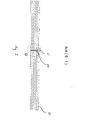
- Fig. 1 shows a printed circuit board comprising SMD elements (ICs 11, 12, 13, 15, 16, microprocessor 14, resistors 9, capacitors 7, 8 etc. in different sizes and types) assembled on the board. Between these elements and around them, there is some space V 2 , V 3 , V 4 (between these elements) and V 1 , V 5 , V 6 , V 7 , V 8 , V 9 , V 10 (around these elements) on the board, but too small to place a lumped heat sink on the board.
- SMD elements ICs 11, 12, 13, 15, 16, microprocessor 14, resistors 9, capacitors 7, 8 etc. in different sizes and types
- Elements placed on the board such as microprocessors 14, ICs 15, 16, power ICs 11, 12, 13 (e.g. for output signal amplifiers) and others, generate heat (hot spots) in a quantity which could be harmful to the electrical function of the printed circuit (by damaging the element itself, other elements or the structure of the board). Since the heat is also transported through the board, even other elements on the board or the board itself can be damaged.
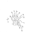
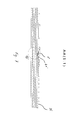
- Fig. 2 shows the board of Fig. 1 , where the typically existing free spaces V 1 , V 2 , V 3 , V 4 , V 5 and V 6 , V 7 , V 8 , V 9 , V 10 are used to be filled (assembled) with a number of heat sink devices 1, 2, 3, 4, 5.
- Said heat sink devices 1, 2, 3, 4, 5, which are assembled automatically by surface mounting machines, can vary in size, depending on the available free space at the respective position on the board and/or depending on the available size and position of the solder pads on the board.
- FIG. 2 even in very small free space or places of the board very small heat sink devices 5 can be placed, whereas in other, somewhat larger places small (but somewhat larger) heat sink devices 4 can be placed, which are a little larger than the aforesaid devices. Furthermore, in even larger places, some (even larger) medium-sized heat sink devices 2 can be placed, and the largest devices 1 are placed in the largest free places on the board.
- Another (differently shaped) heat sink device 3 shows an example of a heat sink device with a larger height than the aforesaid devices.
- the heat sink devices 1, 2, 3, 4, 5 are adapted to receive or absorb heat from the board through their area of contact/contact surface (area of soldering and bottom side) and dissipate the heat by their thermally effective surfaces to the surroundings (air flow generated by a fan, etc.).
- heat sink devices 1, 2, 3, 4, 5 standard SMD parts/elements like resistors, inductors and particularly capacitors (because of their larger height and thus larger surface) can be used.
- Suitable SMD elements and different sizes/types are well-known and shall not be further discussed within this description.
- Such SMD elements, particularly SMD capacitors, acting as heat sink devices are available at reasonably low costs, as such devices are produced in high numbers.
- matching standard SMD elements can easily be chosen, particularly after the printed circuit layout (with its electrical functions) is done, out of different sizes and types (with their thermally effective surfaces). It is further within the scope of the invention to use a number of heat sink devices, even different in size, each having a thermally effective surface larger than the place (because of their height) covered by it, to improve the cooling performance.
- a number of standard SMD elements which are not contacted to the board to have any electrical function, may be used as a number of heat sink devices and may be distributed over the board in small free spaces accordingly acting as a distributed heat sink.
- both connecting surfaces/areas of the heat sink device can be soldered to the board for optimum thermal contact.
- contact surfaces are connected to the electrical paths of the board layout (electrical circuit), it is possible to solder only one contact surface of the heat sink device or to place the heat sink device in such a way that both contact surfaces are soldered to one electrical path without any potential difference, particularly to the ground.
- the performance of dissipating heat from the board is improved.
- the heat sink devices may also be specially produced parts, particularly cuboid blocks, made of heat conducting material, preferably aluminum or copper.
- parts can be produced with even lower costs than standard SMD elements
- Typical sizes (length, width, height) of a heat sink device can vary from less than one to a few millimeters, e.g. length 1-2 mm, width 0.2-0.9 mm and height 0.5-1 mm.
- the board layout may further comprise a layer/plane of copper (not shown) for better cooling of the board.
- the heat sink device(-s) can be contacted to this plane to further improve the cooling performance.
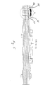
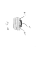
- a heat sink device 1' (as an example of connections to the board N for all heat sink devices 1, 2, 3, 4, 5) by an SMD assembling process, there is a direct and short way (immediate) material contact resulting in a good heat-conducting connection from the board to the heat sink device dissipating heat from the board.
- the heat sink device 1' is soldered to solder pads 26 and 28 on a top face 25 of the printed circuit board N including solder menisci 23 and 24.
- solder pads 26, 28 are also (thermally) connected to a first 27, second 29, third 31, fourth 33 and bottom layer 35 by means of through holes 21 and 22.
- solder pads 26, 28 are only (thermally) connected to the first layer 27 by means of microvias 21' and 22' without any connection to the other layers 29, 31, 33 and 35.
- heat sink device 1' can be connected via solder pads 26, 28 to circuits on the top face in both embodiments only or to any combination of layers as required or possible during the layout of the board.
- the heat sink devices can be placed by standard surface mounting technology, it is possible to plan the filling of free spaces using any combination of differently sized and shaped heat sink devices during the layout of the printed circuit board N, particularly after finishing the step of the layout for electrically functional SMD devices on the board.
- the correct assembling of the (distributed) heat sink devices can be tested (particularly together with the test for the electrically functional SMD devices) by using an automatic optical inspection (AOI) system, which is a standard test procedure for assembled printed circuit boards.
- AOI automatic optical inspection
- distributed heat sink devices as shown above for the top face, can be used on both sides (top and/or bottom) of a printed circuit board in many cases.
- the heat sink devices can be embodied as low profile variants. Even if the thermally effective surface is not much larger than the space covered, the heat sink device can have a better cooling performance because of its better heat conducting properties (as compared to the surface of the board).
Landscapes
- Engineering & Computer Science (AREA)
- Microelectronics & Electronic Packaging (AREA)
- Cooling Or The Like Of Electrical Apparatus (AREA)
- Cooling Or The Like Of Semiconductors Or Solid State Devices (AREA)
Priority Applications (2)
| Application Number | Priority Date | Filing Date | Title |
|---|---|---|---|
| EP11401654.6A EP2600700A1 (fr) | 2011-12-02 | 2011-12-02 | Procédé pour refroidir les cartes de circuits électroniques au moyen de dispositifs montés en applique |
| US13/324,770 US8730677B2 (en) | 2011-12-02 | 2011-12-13 | Method of cooling electronic circuit boards using surface mounted devices |
Applications Claiming Priority (1)
| Application Number | Priority Date | Filing Date | Title |
|---|---|---|---|
| EP11401654.6A EP2600700A1 (fr) | 2011-12-02 | 2011-12-02 | Procédé pour refroidir les cartes de circuits électroniques au moyen de dispositifs montés en applique |
Publications (1)
| Publication Number | Publication Date |
|---|---|
| EP2600700A1 true EP2600700A1 (fr) | 2013-06-05 |
Family
ID=45217462
Family Applications (1)
| Application Number | Title | Priority Date | Filing Date |
|---|---|---|---|
| EP11401654.6A Ceased EP2600700A1 (fr) | 2011-12-02 | 2011-12-02 | Procédé pour refroidir les cartes de circuits électroniques au moyen de dispositifs montés en applique |
Country Status (2)
| Country | Link |
|---|---|
| US (1) | US8730677B2 (fr) |
| EP (1) | EP2600700A1 (fr) |
Cited By (10)
| Publication number | Priority date | Publication date | Assignee | Title |
|---|---|---|---|---|
| WO2014204982A3 (fr) * | 2013-06-19 | 2015-02-26 | SMART Storage Systems, Inc. | Système électronique à extraction de chaleur et son procédé de fabrication |
| US9158349B2 (en) | 2013-10-04 | 2015-10-13 | Sandisk Enterprise Ip Llc | System and method for heat dissipation |
| US9348377B2 (en) | 2014-03-14 | 2016-05-24 | Sandisk Enterprise Ip Llc | Thermal isolation techniques |
| US9470720B2 (en) | 2013-03-08 | 2016-10-18 | Sandisk Technologies Llc | Test system with localized heating and method of manufacture thereof |
| US9485851B2 (en) | 2014-03-14 | 2016-11-01 | Sandisk Technologies Llc | Thermal tube assembly structures |
| US9497889B2 (en) | 2014-02-27 | 2016-11-15 | Sandisk Technologies Llc | Heat dissipation for substrate assemblies |
| US9519319B2 (en) | 2014-03-14 | 2016-12-13 | Sandisk Technologies Llc | Self-supporting thermal tube structure for electronic assemblies |
| US9549457B2 (en) | 2014-02-12 | 2017-01-17 | Sandisk Technologies Llc | System and method for redirecting airflow across an electronic assembly |
| US9898056B2 (en) | 2013-06-19 | 2018-02-20 | Sandisk Technologies Llc | Electronic assembly with thermal channel and method of manufacture thereof |
| US10013033B2 (en) | 2013-06-19 | 2018-07-03 | Sandisk Technologies Llc | Electronic assembly with thermal channel and method of manufacture thereof |
Families Citing this family (1)
| Publication number | Priority date | Publication date | Assignee | Title |
|---|---|---|---|---|
| US9559047B2 (en) * | 2012-10-18 | 2017-01-31 | Infineon Technologies Austria Ag | Passive component as thermal capacitance and heat sink |
Citations (4)
| Publication number | Priority date | Publication date | Assignee | Title |
|---|---|---|---|---|
| GB2259408A (en) * | 1991-09-07 | 1993-03-10 | Motorola Israel Ltd | A heat dissipation device |
| EP0989794A2 (fr) * | 1998-09-22 | 2000-03-29 | Lucent Technologies Inc. | Connexions thermiques montées en surface |
| DE10029094A1 (de) * | 2000-06-13 | 2001-12-20 | Sli Miniature Lighting Gmbh | SMD-Kühler, insbesondere für thermisch hochintegrierte Schaltungen |
| US6621705B1 (en) * | 2002-04-12 | 2003-09-16 | Cisco Technology, Inc. | Miniature surface mount heatsink element and method of use |
Family Cites Families (13)
| Publication number | Priority date | Publication date | Assignee | Title |
|---|---|---|---|---|
| US5467251A (en) * | 1993-10-08 | 1995-11-14 | Northern Telecom Limited | Printed circuit boards and heat sink structures |
| US5475263A (en) * | 1994-02-14 | 1995-12-12 | Delco Electronics Corp. | Thick film hybrid multilayer circuit |
| US5708566A (en) * | 1996-10-31 | 1998-01-13 | Motorola, Inc. | Solder bonded electronic module |
| US5978223A (en) * | 1998-02-09 | 1999-11-02 | International Business Machines Corporation | Dual heat sink assembly for cooling multiple electronic modules |
| US6212071B1 (en) * | 1999-08-20 | 2001-04-03 | Lucent Technologies, Inc. | Electrical circuit board heat dissipation system |
| JP3573034B2 (ja) * | 1999-11-17 | 2004-10-06 | 日本電気株式会社 | 多層プリント配線板およびその放熱構造 |
| JP3923703B2 (ja) * | 2000-03-29 | 2007-06-06 | ローム株式会社 | 放熱手段を有するプリント配線板 |
| JP2003289191A (ja) * | 2002-03-28 | 2003-10-10 | Denso Corp | 電子制御装置 |
| US6882537B2 (en) * | 2002-12-23 | 2005-04-19 | Eastman Kodak Company | Electrical assemblage and method for removing heat locally generated therefrom |
| US6770967B2 (en) * | 2002-12-23 | 2004-08-03 | Eastman Kodak Company | Remote thermal vias for densely packed electrical assemblage |
| US8383946B2 (en) * | 2010-05-18 | 2013-02-26 | Joinset, Co., Ltd. | Heat sink |
| US8391010B2 (en) * | 2010-08-19 | 2013-03-05 | Apple Inc. | Internal frame optimized for stiffness and heat transfer |
| US8649179B2 (en) * | 2011-02-05 | 2014-02-11 | Laird Technologies, Inc. | Circuit assemblies including thermoelectric modules |
-
2011
- 2011-12-02 EP EP11401654.6A patent/EP2600700A1/fr not_active Ceased
- 2011-12-13 US US13/324,770 patent/US8730677B2/en not_active Expired - Fee Related
Patent Citations (4)
| Publication number | Priority date | Publication date | Assignee | Title |
|---|---|---|---|---|
| GB2259408A (en) * | 1991-09-07 | 1993-03-10 | Motorola Israel Ltd | A heat dissipation device |
| EP0989794A2 (fr) * | 1998-09-22 | 2000-03-29 | Lucent Technologies Inc. | Connexions thermiques montées en surface |
| DE10029094A1 (de) * | 2000-06-13 | 2001-12-20 | Sli Miniature Lighting Gmbh | SMD-Kühler, insbesondere für thermisch hochintegrierte Schaltungen |
| US6621705B1 (en) * | 2002-04-12 | 2003-09-16 | Cisco Technology, Inc. | Miniature surface mount heatsink element and method of use |
Cited By (12)
| Publication number | Priority date | Publication date | Assignee | Title |
|---|---|---|---|---|
| US9470720B2 (en) | 2013-03-08 | 2016-10-18 | Sandisk Technologies Llc | Test system with localized heating and method of manufacture thereof |
| WO2014204982A3 (fr) * | 2013-06-19 | 2015-02-26 | SMART Storage Systems, Inc. | Système électronique à extraction de chaleur et son procédé de fabrication |
| US9313874B2 (en) | 2013-06-19 | 2016-04-12 | SMART Storage Systems, Inc. | Electronic system with heat extraction and method of manufacture thereof |
| US9898056B2 (en) | 2013-06-19 | 2018-02-20 | Sandisk Technologies Llc | Electronic assembly with thermal channel and method of manufacture thereof |
| US10013033B2 (en) | 2013-06-19 | 2018-07-03 | Sandisk Technologies Llc | Electronic assembly with thermal channel and method of manufacture thereof |
| US9158349B2 (en) | 2013-10-04 | 2015-10-13 | Sandisk Enterprise Ip Llc | System and method for heat dissipation |
| US9549457B2 (en) | 2014-02-12 | 2017-01-17 | Sandisk Technologies Llc | System and method for redirecting airflow across an electronic assembly |
| US9497889B2 (en) | 2014-02-27 | 2016-11-15 | Sandisk Technologies Llc | Heat dissipation for substrate assemblies |
| US9848512B2 (en) | 2014-02-27 | 2017-12-19 | Sandisk Technologies Llc | Heat dissipation for substrate assemblies |
| US9348377B2 (en) | 2014-03-14 | 2016-05-24 | Sandisk Enterprise Ip Llc | Thermal isolation techniques |
| US9485851B2 (en) | 2014-03-14 | 2016-11-01 | Sandisk Technologies Llc | Thermal tube assembly structures |
| US9519319B2 (en) | 2014-03-14 | 2016-12-13 | Sandisk Technologies Llc | Self-supporting thermal tube structure for electronic assemblies |
Also Published As
| Publication number | Publication date |
|---|---|
| US20130141873A1 (en) | 2013-06-06 |
| US8730677B2 (en) | 2014-05-20 |
Similar Documents
| Publication | Publication Date | Title |
|---|---|---|
| US8730677B2 (en) | Method of cooling electronic circuit boards using surface mounted devices | |
| US8971045B1 (en) | Module having at least one thermally conductive layer between printed circuit boards | |
| US5933324A (en) | Apparatus for dissipating heat from a conductive layer in a circuit board | |
| US9408308B2 (en) | Heat dissipating high power systems | |
| CN105188318A (zh) | 散热装置、电子设备及制造方法 | |
| CN201213333Y (zh) | 一种散热器件、电路板组合装置及通信设备 | |
| US12137545B2 (en) | Electromagnetic shield of an integrated circuit package | |
| US20120325540A1 (en) | Footprint on pcb for leadframe-based packages | |
| US7443025B2 (en) | Thermally improved placement of power-dissipating components onto a circuit board | |
| CN110113874B (zh) | Pcb元器件及其制作方法 | |
| JP2003188565A (ja) | 表面実装用電子部品の放熱構造 | |
| EP2276329A1 (fr) | Carte de circuit électronique dotée d'un condensateur thermique | |
| CN110073726B (zh) | 印刷布线基板、空调机以及印刷布线基板的制造方法 | |
| JP2005150283A (ja) | Bgaパッケージ | |
| US11219137B2 (en) | Electronic device and power module thereof | |
| JP2002151634A (ja) | 基板放熱装置 | |
| CN100401506C (zh) | 球单阵列封装芯片的散热装置及其应用 | |
| CN103929876A (zh) | 一种印制电路板组合焊盘 | |
| CN221224990U (zh) | 一种用于磁共振系统的功率吸收负载 | |
| CN205789112U (zh) | 电路板及应用该电路板的存储器 | |
| JP4952904B2 (ja) | プリント配線基板とこれを備えたモータ制御装置 | |
| KR20140129804A (ko) | 방열기판 | |
| JP7062473B2 (ja) | アンテナモジュール | |
| KR20080004734A (ko) | 발열소자의 방열구조 | |
| JP2006514429A (ja) | 電子器具用の放熱装置 |
Legal Events
| Date | Code | Title | Description |
|---|---|---|---|
| PUAI | Public reference made under article 153(3) epc to a published international application that has entered the european phase |
Free format text: ORIGINAL CODE: 0009012 |
|
| AK | Designated contracting states |
Kind code of ref document: A1 Designated state(s): AL AT BE BG CH CY CZ DE DK EE ES FI FR GB GR HR HU IE IS IT LI LT LU LV MC MK MT NL NO PL PT RO RS SE SI SK SM TR |
|
| AX | Request for extension of the european patent |
Extension state: BA ME |
|
| 17P | Request for examination filed |
Effective date: 20131202 |
|
| RBV | Designated contracting states (corrected) |
Designated state(s): AL AT BE BG CH CY CZ DE DK EE ES FI FR GB GR HR HU IE IS IT LI LT LU LV MC MK MT NL NO PL PT RO RS SE SI SK SM TR |
|
| 17Q | First examination report despatched |
Effective date: 20140108 |
|
| APBK | Appeal reference recorded |
Free format text: ORIGINAL CODE: EPIDOSNREFNE |
|
| APBN | Date of receipt of notice of appeal recorded |
Free format text: ORIGINAL CODE: EPIDOSNNOA2E |
|
| APBR | Date of receipt of statement of grounds of appeal recorded |
Free format text: ORIGINAL CODE: EPIDOSNNOA3E |
|
| APAF | Appeal reference modified |
Free format text: ORIGINAL CODE: EPIDOSCREFNE |
|
| APBT | Appeal procedure closed |
Free format text: ORIGINAL CODE: EPIDOSNNOA9E |
|
| STAA | Information on the status of an ep patent application or granted ep patent |
Free format text: STATUS: THE APPLICATION HAS BEEN REFUSED |
|
| 18R | Application refused |
Effective date: 20201221 |