EP2602930B1 - Émetteur et son procédé de commande - Google Patents
Émetteur et son procédé de commande Download PDFInfo
- Publication number
- EP2602930B1 EP2602930B1 EP11814220.7A EP11814220A EP2602930B1 EP 2602930 B1 EP2602930 B1 EP 2602930B1 EP 11814220 A EP11814220 A EP 11814220A EP 2602930 B1 EP2602930 B1 EP 2602930B1
- Authority
- EP
- European Patent Office
- Prior art keywords
- signal
- current
- current source
- variable
- switching element
- Prior art date
- Legal status (The legal status is an assumption and is not a legal conclusion. Google has not performed a legal analysis and makes no representation as to the accuracy of the status listed.)
- Not-in-force
Links
- 238000000034 method Methods 0.000 title description 5
- 230000000295 complement effect Effects 0.000 claims description 5
- 238000010586 diagram Methods 0.000 description 40
- 230000014509 gene expression Effects 0.000 description 21
- 239000010752 BS 2869 Class D Substances 0.000 description 11
- 230000005540 biological transmission Effects 0.000 description 5
- 239000003990 capacitor Substances 0.000 description 5
- 230000003071 parasitic effect Effects 0.000 description 4
- 230000001413 cellular effect Effects 0.000 description 3
- 238000006243 chemical reaction Methods 0.000 description 3
- 230000003321 amplification Effects 0.000 description 2
- 239000000284 extract Substances 0.000 description 2
- 230000002349 favourable effect Effects 0.000 description 2
- 238000003199 nucleic acid amplification method Methods 0.000 description 2
- 238000005070 sampling Methods 0.000 description 2
- 229910002704 AlGaN Inorganic materials 0.000 description 1
- 239000008186 active pharmaceutical agent Substances 0.000 description 1
- 230000007423 decrease Effects 0.000 description 1
- 238000007599 discharging Methods 0.000 description 1
- 230000000694 effects Effects 0.000 description 1
- 230000005669 field effect Effects 0.000 description 1
Images






Classifications
-
- H—ELECTRICITY
- H04—ELECTRIC COMMUNICATION TECHNIQUE
- H04W—WIRELESS COMMUNICATION NETWORKS
- H04W52/00—Power management, e.g. Transmission Power Control [TPC] or power classes
- H04W52/02—Power saving arrangements
- H04W52/0209—Power saving arrangements in terminal devices
-
- H—ELECTRICITY
- H03—ELECTRONIC CIRCUITRY
- H03F—AMPLIFIERS
- H03F1/00—Details of amplifiers with only discharge tubes, only semiconductor devices or only unspecified devices as amplifying elements
- H03F1/02—Modifications of amplifiers to raise the efficiency, e.g. gliding Class A stages, use of an auxiliary oscillation
- H03F1/0205—Modifications of amplifiers to raise the efficiency, e.g. gliding Class A stages, use of an auxiliary oscillation in transistor amplifiers
- H03F1/0211—Modifications of amplifiers to raise the efficiency, e.g. gliding Class A stages, use of an auxiliary oscillation in transistor amplifiers with control of the supply voltage or current
- H03F1/0216—Continuous control
- H03F1/0222—Continuous control by using a signal derived from the input signal
-
- H—ELECTRICITY
- H03—ELECTRONIC CIRCUITRY
- H03F—AMPLIFIERS
- H03F3/00—Amplifiers with only discharge tubes or only semiconductor devices as amplifying elements
- H03F3/189—High-frequency amplifiers, e.g. radio frequency amplifiers
-
- H—ELECTRICITY
- H03—ELECTRONIC CIRCUITRY
- H03F—AMPLIFIERS
- H03F3/00—Amplifiers with only discharge tubes or only semiconductor devices as amplifying elements
- H03F3/20—Power amplifiers, e.g. Class B amplifiers, Class C amplifiers
- H03F3/21—Power amplifiers, e.g. Class B amplifiers, Class C amplifiers with semiconductor devices only
- H03F3/217—Class D power amplifiers; Switching amplifiers
-
- H—ELECTRICITY
- H03—ELECTRONIC CIRCUITRY
- H03F—AMPLIFIERS
- H03F3/00—Amplifiers with only discharge tubes or only semiconductor devices as amplifying elements
- H03F3/20—Power amplifiers, e.g. Class B amplifiers, Class C amplifiers
- H03F3/24—Power amplifiers, e.g. Class B amplifiers, Class C amplifiers of transmitter output stages
-
- H—ELECTRICITY
- H03—ELECTRONIC CIRCUITRY
- H03F—AMPLIFIERS
- H03F3/00—Amplifiers with only discharge tubes or only semiconductor devices as amplifying elements
- H03F3/20—Power amplifiers, e.g. Class B amplifiers, Class C amplifiers
- H03F3/24—Power amplifiers, e.g. Class B amplifiers, Class C amplifiers of transmitter output stages
- H03F3/245—Power amplifiers, e.g. Class B amplifiers, Class C amplifiers of transmitter output stages with semiconductor devices only
-
- H—ELECTRICITY
- H03—ELECTRONIC CIRCUITRY
- H03F—AMPLIFIERS
- H03F2200/00—Indexing scheme relating to amplifiers
- H03F2200/336—A I/Q, i.e. phase quadrature, modulator or demodulator being used in an amplifying circuit
-
- H—ELECTRICITY
- H03—ELECTRONIC CIRCUITRY
- H03F—AMPLIFIERS
- H03F2200/00—Indexing scheme relating to amplifiers
- H03F2200/408—Indexing scheme relating to amplifiers the output amplifying stage of an amplifier comprising three power stages
-
- H—ELECTRICITY
- H03—ELECTRONIC CIRCUITRY
- H03F—AMPLIFIERS
- H03F2200/00—Indexing scheme relating to amplifiers
- H03F2200/91—Indexing scheme relating to amplifiers the amplifier has a current mode topology
Definitions
- the present invention relates to a transmitter used for a communication device, such as a cellular phone or a wireless LAN, and a method for controlling the same, and more particularly, to a transmitter having an excellent power efficiency, and a method for controlling the same.
- a transmission unit of a communication device such as a cellular phone or a wireless LAN, is required to operate with low power consumption.
- Such a transmission unit of a communication device is required to operate with low power consumption regardless of the magnitude of output power, and is also required to ensure a high accuracy of transmission signals.
- a power amplifier disposed at a final stage of a transmission unit of a communication device occupies 50% or more of the power consumption of the entire transmitter. For this reason, the power amplifier disposed at the final stage of the transmission unit of the communication device needs to have a high power efficiency.
- the switching amplifier receives pulse-shape signals.
- the switching amplifier amplifies the power of received pulse-shape signals while maintaining the pulse shape.
- the pulse-shape signals amplified by the switching amplifier are transmitted from an antenna after frequency components other than desired frequency components are sufficiently suppressed by a filter element.
- CMCD current mode class-D amplifier
- Fig. 17 is a circuit block diagram showing a configuration example of a CMCD 6.
- the CMCD 6 includes variable current sources 61 and 62, switching elements 63 and 64, a load 65, and a filter circuit 66.
- the variable current sources 61 and 62 are connected in parallel with a power supply VDD.
- the switching element 63 is connected between the variable current source 61 and a ground GND.
- the switching element 64 is connected between the variable current source 62 and the ground GND.
- the load 65 and the filter circuit 66 are connected in parallel between an output terminal of the switching element 63 and an output terminal of the switching element 64.
- Pulse signals are input to control terminals of the switching elements 63 and 64.
- the pulse signal input to the control terminal of the switching element 64 is a signal complementary to the pulse signal input to the control terminal of the switching element 63.
- the current source connected to the switching element in the OFF state supplies a current to the load 65 and the filter circuit 66.
- a current from the current source connected to the switching element flows into the switching element in the ON state. Further, a current from the current source connected to the switching element in the OFF state flows into the switching element in the ON state through the load 65 and the filter circuit 66.
- a typical class-AB power amplifier and the like require a bias current.
- the CMCD requires no bias current. Accordingly, a power loss in the CMCD is equal to the sum of a switching loss generated during charging/discharging to/from a parasitic capacitance and a heat loss generated in a parasitic resistance. Accordingly, when the parasitic capacitance and the parasitic resistance are ideally zero, the power loss of the CMCD is "0" .
- Fig. 18 is a circuit block diagram showing a configuration example of the transmitter 700 incorporating the CMCD 6.
- the transmitter 700 includes an RF signal generator 71, a driver amplifier 72, and the CMCD 6.
- the RF signal generator 71 includes a digital baseband (hereinafter referred to as "DBB") 711, sigma-delta modulators 712 and 713, a digital up-converter 714, and an inverter 715.
- DBB 711 generates a radio signal which is a multi-bit signal of 10 bits or more.
- a pulse signal representing information by two states (1 bit) of high and low can be input to the CMCD 6. Accordingly, it is necessary to convert the multi-bit signal output from the DBB 711 into a 1-bit signal that is subjected to over-sampling in advance.
- the sigma-delta modulators 712 and 713 are used as means for converting a multi-bit signal into a 1-bit signal by over-sampling.
- Each signal output from the sigma-delta modulators 712 and 713 is output as a pulse signal through the digital up-converter 714.
- the pulse signal output from the digital up-converter 714 is divided into two signals. One of the divided pulse signals is inverted by the inverter 715.
- a non-inverted pulse signal is input to the switching element 63 of the CMCD 6 through the driver amplifier 72.
- the inverted pulse signal is input to the switching element 64 of the CMCD 6 through the driver amplifier 72.
- the sigma-delta modulators 712 and 713 described above can favorably maintain noise characteristics in the vicinity of a desired frequency band. Accordingly, in this configuration example, a multi-bit radio signal can be converted into a pulse signal and the pulse signal can be input to the CMCD 6, while maintaining satisfactory noise characteristics.
- Non Patent Literature 1 R. Leberer, R. Reber, and M. Oppermann, "An AlGaN/GaN Class-S Amplifier for RF-Communication Signals", IEEE/MTT-S International Microwave Symposium 2008, June 2008, pp. 85-88 .
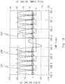
- Fig. 19 is a graph showing output voltage waveforms of the switching elements 63 and 64 when a W-CDMA signal is converted into a 1-bit signal by sigma-delta modulation.
- a curve L63 represents the output voltage waveform of the switching element 63.
- a curve L64 represents the output voltage waveform of the switching element 64.
- a line G63 represents the waveform of the pulse signal input to the control terminal of the switching element 63.
- each of the switching elements 63 and 64 is composed of an FET element.
- a voltage at the drain terminal of the FET element fluctuates to the minus side.
- the FET element is turned off when the voltage at the drain terminal is equal to or higher than 0 and a gate potential is smaller than a threshold (Vth) with respect to a source potential.
- Vth threshold
- the channel is opened and comes into a conductive state.
- a power Pdrv necessary to drive the gate of the switching element is expressed by the following expression (1).
- Cgs represents a gate capacitance
- Vgs represents a potential difference between the ON signal and the OFF signal to be applied to the gate
- f represents a switching frequency.
- the power Pdrv is proportional to the square of the potential difference Vgs. In a typical device, several volts are required as the potential difference Vgs. The power Pdrv at this time is about several watts. Accordingly, in the state where the potential difference Vgs is several tens of volts, the power Pdrv is several hundred watts, resulting in a considerable increase in power consumption.
- the present invention has been made in view of the above-mentioned problems, and an object of the present invention is to provide a transmitter having favorable noise characteristics and excellent power efficiency, and a method for controlling the same.
- CMCD current mode class-D amplifier
- Fig. 1 is a block diagram showing a configuration of a transmitter 100 according to the first exemplary embodiment.
- the transmitter 100 includes an RF signal generator 1a and a current mode class-D amplifier 2a.
- the RF signal generator 1a includes a digital baseband (hereinafter referred to as "DBB") 11, an IQ modulator 12, and an amplitude phase signal detector 13.
- the DBB 11 generates IQ signals.
- the IQ modulator 12 converts the IQ signals into an RF signal RF(t) by IQ modulation.
- t is a variable representing time.
- the RF signal RF(t) is generally expressed by the following expression (2) using an amplitude signal r(t) and a phase signal th(t).
- RF t r t ⁇ th t
- phase signal th(t) is expressed by the following expression (3).
- th t cos ⁇ c ⁇ t + theta t
- ⁇ c an angular velocity obtained by multiplying a carrier frequency by 2 ⁇
- theta(t) is a phase variation.
- the amplitude phase signal detector 13 separates and extracts the amplitude signal r(t) and the phase signal th(t) which are included in the RF signal RF(t).
- the amplitude phase signal detector 13 outputs the amplitude signal r(t) and a rectangular phase signal Rth(t) which is obtained by forming the phase signal th(t) into a rectangular shape.
- the phase signal th(t) is equal to or greater than 0
- the value of the rectangular phase signal Rth(t) is "1”.
- the phase signal th(t) is smaller than 0, the value of the rectangular phase signal Rth(t) is "0".
- a relationship as expressed by the following expression (4) is established between the phase signal th(t) and the rectangular phase signal Rth(t).
- Rth t th t + dis t where dis(t) is composed of a harmonic component of th(t).
- the CMCD 2a includes variable current sources 21 and 22, switching elements 23 and 24, a load 25, and a filter circuit 26.
- the variable current sources 21 and 22 are connected in parallel with a power supply VDD.
- the switching element 23 is connected between the variable current source 21 and a ground GND.
- the switching element 24 is connected between the variable current source 22 and the ground GND.
- the load 25 and the filter circuit 26 are connected in parallel between an output terminal of the switching element 23 and an output terminal of the switching element 24.
- the amplitude signal r(t) is input to the variable current sources 21 and 22 as a control signal.
- the rectangular phase signal Rth(t) is input to the switching element 23 as a control signal.
- a complementary signal of the rectangular phase signal Rth(t) is input to the switching element 24 as a control signal through an inverter INV.
- a flow of a current in the CMCD 2a will now be described.
- a description is given of the case where the switching element 23 is turned off and the switching element 24 is turned on.
- a current flows into the switching element 24 from the variable current source 21 through the load 25 and the filter circuit 26.
- a current flows into the switching element 24 from the variable current source 22.
- a description is given of the case where the switching element 23 is turned on and the switching element 24 is turned off.
- a current flows into the switching element 23 from the variable current source 22 through the load 25 and the filter circuit 26.
- a current flows into the switching element 23 from the variable current source 21. That is, the pulse-like current, the flow direction of which is reversed so as to correspond to opening and closing operations of the switching elements 23 and 24, is input to the load 25 and the filter circuit 26.
- Fig. 2 is a circuit diagram showing a configuration example of the filter circuit 26.
- the filter circuit 26 includes an inductor L1 and a capacitor C1.
- the inductor L1 and the capacitor C1 are connected in parallel.
- the impedance of the filter circuit 26 increases (closer to an open condition) toward a resonance point.
- the impedance of the filter circuit 26 decreases (closer to a short-circuit condition) as the distance from the resonance point.
- Suitable setting of a constant of each element that forms the filter circuit 26 allows the resonance point of the filter circuit 26 to match a desired bandwidth of a radio signal. As a result, a state close to the open condition is achieved for the desired bandwidth. On the other hand, a state close to the short-circuit condition is set for bandwidths other than the desired bandwidth. Accordingly, only the desired band component of the pulse current is supplied through the load 25. As a result, the radio signal from which undesired harmonic components are removed is extracted.
- a current value output from the variable current sources 21 and 22 is represented by I(t).
- a control signal given to each switching element is represented by P(t).
- the control signal P(t) is a 1-bit signal having two states of "1" and "-1".
- the switching element 23 is turned on.
- the switching element 24 is turned on.
- a current signal Dout(t) output to each of the load 25 and filter circuit 26 is expressed by the following expression (5).
- Dout t I t ⁇ P t
- the resonance frequency of the filter circuit 26 is set to correspond to r(t) ⁇ th(t) that is included in Dout(t). This allows only r(t) ⁇ th(t) to be input to the load 25. In other words, only the RF signal can be extracted by the CMCD 2a.
- Fig. 3 is a graph showing an output waveform of the CMCD 2a.
- the CMCD 2a can resolve the phenomenon that the output voltage fluctuates greatly to the minus side, while performing an amplitude modulation.
- FET elements are used as the switching elements 23 and 24
- a voltage difference of about several V between high and low signals to be supplied to gates is sufficient. Accordingly, in the transmitter 100 including the CMCD 2a, driving power can be minimized.
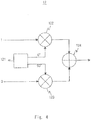
- Fig. 4 is a block diagram showing a configuration example of the IQ modulator 12.
- the IQ modulator 12 includes an IQ local oscillator 121, a mixer 122, a mixer 123, and a synthesizer 124.
- the IQ local oscillator 121 generates two sinusoidal wave voltage signals having a phase difference of 90° therebetween. These two sinusoidal wave voltage signals have a frequency equal to the carrier frequency of the RF signal.
- the mixer 122 and the mixer 123 output the product of the signals input from two input terminals.
- the mixer 122 receives an I signal from the DBB 11 and a sinusoidal wave voltage signal generated in the IQ local oscillator 121.
- the mixer 123 receives a Q signal from the DBB 11 and a sinusoidal wave voltage signal generated in the local oscillator.
- the synthesizer 124 outputs the sum of the signals input from the two input terminals.
- the mixer 122 outputs the product of a voltage signal Vlo_i and the voltage Vbb_i of the baseband signal I.
- the mixer 123 outputs the product of a voltage signal Vlo_q and the voltage Vbb_q of the baseband signal Q.
- An output voltage signal Vmix1 of the mixer 122 is expressed by the following expression (11).
- An output voltage signal Vmix2 of the mixer 123 is expressed by the following expression (12).
- the synthesizer 124 outputs the sum of the output voltage signal Vmix1 of the mixer 122 and the output voltage signal Vmix2 of the mixer 123.
- An output voltage signal Vcomb of the synthesizer 124 is expressed by the following expression (13).
- Vcomb ABcos ⁇ c + ⁇ b t + ⁇
- the output voltage signal Vcomb is an RF signal obtained by increasing the frequency by ⁇ c from the angular frequency of the baseband signal.
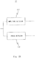
- Fig. 5A is a block diagram showing a configuration example of the amplitude phase signal detector 13.
- the amplitude phase signal detector 13 includes an amplitude detector 131 and a phase detector 132.
- Fig. 5B is a circuit diagram showing a configuration example of the amplitude detector 131.
- the amplitude detector 131 includes a diode D13, a resistor R13, and a capacitor C13.
- the diode D13 outputs a current which is proportional to the square of the input voltage. Accordingly, when the RF signal is input to the diode, as the amplitude value increases, the time average value of the current value output from the diode D13 increases.
- the resistor R13 and the capacitor C13 which are connected to the subsequent stage of the diode D13, form a filter circuit. This filter circuit extracts only a DC component included in the output current of the diode D13.
- the extracted DC component is equivalent to the time average value of the output current of the diode D13. That is, as the amplitude value of the RF signal increases, the value of the DC component increases.
- the DC component of the output current of the diode D13 is a one-to-one function that increases monotonously with respect to the amplitude value of the RF signal input to the diode D13. Accordingly, the extracted DC component makes it possible to extract the amplitude information included in the RF signal.
- Fig. 5C is a block diagram showing a configuration example of the phase detector 132.
- the phase detector 132 includes a comparator CMP.
- the comparator CMP outputs a high signal when the input signal takes a positive value, and outputs a low signal when the input signal takes a negative value.
- the RF signal takes a positive value
- the RF signal takes a negative value.
- the phase detector 132 outputs the high signal when the phase of the RF signal is in the range of 0° to 180°, and outputs the low signal when the phase of the RF signal is in the range of 180° to 360°.
- the output of the comparator CMP is ideally a rectangular wave.
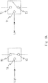
- Fig. 6A is a configuration diagram showing an operation of the switching element 23.
- the switching element 23 has a control terminal T1, a signal terminal T2, and a signal terminal T3.
- the signal terminal T2 and the signal terminal T3 are brought into the short-circuit state (ON state).
- the signal terminal T2 and the signal terminal T3 are brought into the non-connected state (OFF state).
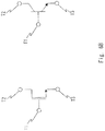
- Fig. 6B is a circuit diagram showing a configuration example of the switching element 23.
- the switching element 23 can be implemented using a field-effect transistor (FET) or a bipolar transistor.
- FET field-effect transistor
- the control terminal T1 corresponds to a gate terminal of an FET or a base terminal of a bipolar transistor.
- the signal terminal T2 corresponds to a source terminal of an FET or an emitter terminal of a bipolar transistor.
- the signal terminal T3 corresponds to a drain terminal of an FET or a collector terminal of a bipolar transistor.
- the operation and configuration of the switching element 24 are similar to those of the switching element 23, so the description thereof is omitted.
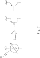
- Fig. 7 is a circuit diagram showing a configuration example of the variable current source 21.
- the variable current source 21 is composed of an FET.
- the control signal of the variable current source 21 is given to the gate terminal of the FET.
- the value of a current flowing between the drain and the source of the FET is proportional to the square of a difference between a gate potential and a threshold voltage in a saturation region. That is, the gate potential and the current flowing between the drain and the source have a 1:1 relation. Accordingly, the current can be controlled by the gate potential.
- the variable current source 21 can also be composed of a bipolar transistor.
- the configuration of the variable current source 22 is similar to that of the variable current source 21, so the description thereof is omitted.
- Fig. 8 is a circuit diagram showing another configuration example of the variable current source 21.
- the variable current source 21 shown in Fig. 8 includes a decoder 211 and a pulse variable current source 212.
- the pulse variable current source 212 includes one or more DC current sources Iv1 to IvN and current switches S1 to SN respectively connected to output terminals of the DC current sources Iv1 to IvN.
- a current switch Sn (n is an integer equal to or greater than 1) switches an output destination of a current output from the DC current source Ivn to a ground node or an output node of the pulse variable current source 212.
- the current output from the pulse variable current source 212 is equal to the sum of currents output from the DC current sources connected to the output node of the pulse variable current source 212 through the current switchs.
- the amplitude signal r(t) generated in the RF signal generator 1a is input to the decoder 211.
- the pulse variable current source 212 is provided with the DC current sources Iv1 to IvN.
- a current value In of the DC current source Ivn is weighted by a power of 2.
- the current value In is represented by 10 ⁇ 2 -n .
- 10 represents a given value.
- the decoder 211 sequentially allocates the bits of the amplitude signal r(t) from the highest bit as control signals for the current switches S1 to SN respectively connected to the DC current sources Iv1 to IvN.
- the amplitude signal r(t) is an analog signal
- this analog signal is converted into an N-bit digital signal by AD conversion.
- the digital signal generated by AD conversion is input to the decoder 211.
- Fig. 9 is a block diagram showing a configuration example of the current switch Sn.
- the current switch Sn includes a diode Ds and a current switching element SW.
- the current switching element SW may have a configuration shown in Fig. 6B , for example.
- the current switching element SW is disposed between an anode-side terminal of the diode Ds and a ground potential (or a given DC potential).
- the anode-side terminal of the diode Ds is further connected to a terminal A.
- a cathode-side terminal of the diode Ds is connected to a terminal B.
- Fig. 10 is a block diagram showing a configuration example of the DC current source Ivn.
- the DC current source Ivn includes a variable DC voltage source 41, an inductor 42, a current sensor 43, and a comparison controller 44.
- a current output from the variable DC voltage source 41 is output through the inductor 42 and the current sensor 43.
- the current sensor 43 detects the magnitude of the current flowing through the current sensor 43.
- the comparison controller 44 controls the voltage of the variable DC voltage source 41 so that the current value detected by the current sensor 43 becomes a desired value.
- the transfer function F(s) is a transfer function of a lowpass filter in which a 3dB cutoff frequency is given by Rload/(2 ⁇ Ladd).
- the control signal given to the variable DC voltage source 41 is updated at a speed sufficiently higher than the above-mentioned cutoff frequency, thereby minimizing the variation characteristic of the output current lout.
- Fig. 11 is a block diagram showing a specific example of the configuration of the DC current source Ivn.
- the variable DC voltage source 41 has a configuration in which switching elements Sv1 and Sv2 are disposed in series between a DC voltage source 51 and a ground terminal.
- the switching elements Sv1 and Sv2 may have a configuration shown in Fig. 6B , for example.
- the switching element Sv1 located on the power supply side and the switching element Sv2 located on the ground side perform complementary opening/closing operations. Specifically, when one of the switching elements Sv1 and Sv2 is turned on, the other of the switching elements is turned off. When the switching element Sv1 is turned on, the output voltage of the variable DC voltage source 41 is equal to the power supply voltage. On the other hand, when the switching element Sv2 is turned on, the output voltage of the variable DC voltage source 41 is equal to the ground potential.
- the current sensor 43 includes a resistor Rs and a differential input type amplifier AMP.
- the differential input type amplifier AMP receives voltage information at both terminal nodes of the resistor Rs. When the input current flows through the resistor Rs, a voltage difference which is equal to the product of the current and the resistance value is generated at the both ends of the resistor Rs.
- the differential input type amplifier AMP amplifies and outputs the voltage difference (in this exemplary embodiment, the amplification factor is a positive value). Note that the voltage difference between the both ends of the resistor Rs and the output value of the differential input type amplifier AMP have a 1:1 relation. That is, the current sensor 43 is capable of converting the current value of the input current into a voltage value and outputting the voltage value.
- the comparison controller 44 includes a voltage comparator 52 and a coder 53.
- the voltage comparator 52 compares the voltage value output from the current sensor 43 with an internal reference value. The case where the output from the current sensor 43 is larger than the internal reference value indicates that the amount of current flowing through the current sensor 43 is larger than a desired value.
- the coder 53 outputs a control signal that brings the ground-side switching element Sv2, which forms the variable DC voltage source 41, into the ON state, and brings the power-supply-side switching element Sv1 into the OFF state.
- the case where the output from the current sensor 43 is smaller than the internal reference value indicates that the amount of current flowing through the current sensor 43 is smaller than the desired value.
- the coder 53 outputs a control signal which brings the ground-side switching element Sv2, which forms the variable DC voltage source 41, into the OFF state, and brings the power-supply-side switching element Sv1 into the ON state.
- the comparison controller 44 operates in synchronization with an external clock signal from an external clock signal source CLKO. Specifically, the cycle of performing a comparison operation in the voltage comparator 52 and updating the control signal to be supplied to the variable DC voltage source 41 is equal to the cycle of the external clock signal source CLKO. Even when the load connected to the DC current source Ivn is temporally varied, the comparison controller is caused to operate using the clock signal source that generates a clock signal having a sufficiently shorter cycle than the variation cycle. This allows the control signal for the variable DC voltage source 41 to be updated in a period shorter than the variation cycle of the load. The operation described above allows the DC current source Ivn to continuously output a desired DC current.
- Fig. 12 is a block diagram showing a configuration of a CMCD 2b which is a first configuration transformed example of the CMCD.
- the CMCD 2b includes a variable current source 31, inductors 32 and 33, and the switching elements 23 and 24.
- the switching elements 23 and 24 are similar to those of the CMCD 2a.
- One end of the variable current source 31 is connected to the power supply VDD.
- the other end of the variable current source 31 is connected to the switching element 23 through the inductor 32, and is also connected to the switching element 24 through the inductor 33.
- the variable current source 31 is controlled by the amplitude signal r(t), for example.
- the other components of the CMCD 2b are similar to those of the CMCD 2a, so the description thereof is omitted.
- the inductors 32 and 33 suppress the variation of the current value. Accordingly, the inductors 32 and 33 provide a current source operation in a pseudo manner.
- the CMCD 2b according to this configuration example operates in a similar manner to the CMCD 2a shown in Fig. 1 in which two current sources are directly connected to two switching elements, respectively.
- Fig. 13 is a block diagram showing a configuration of a CMCD 2c which is the second configuration transformed example of the CMCD.
- the CMCD 2c has a configuration in which a filter circuit 34 is added to the CMCD 2b shown in Fig. 12 .
- the filter circuit 34 is disposed between the variable current source 31 and the inductors 32 and 33.
- the other components of the CMCD 2c are similar to those of the CMCD 2b, so the description thereof is omitted.
- the filter circuit 34 removes undesired harmonic components generated in the variable current source 31.
- Fig. 14 is a block diagram showing a configuration of a CMCD 2d which is the third configuration transformed example of the CMCD.
- the CMCD 2d has a configuration in which the variable current source 31 of the CMCD 2b shown in Fig. 12 is replaced with a variable voltage source 35.
- the inductors 32 and 33 suppress the variation of the current value, as in the CMCD 2b shown in Fig. 12 . Accordingly, the inductors 32 and 33 provide a current source operation in a pseudo manner.
- the other components of the CMCD 2d are similar to those of the CMCD 2b, so the description thereof is omitted.
- the CMCD 2d according to this configuration example operates in a similar manner to the CMCD 2a shown in Fig. 1 in which two current sources are directly connected to two switching elements, respectively.
- Fig. 15 is a block diagram showing a configuration of a transmitter 200 according to the second exemplary embodiment.
- the transmitter 200 has a configuration in which the RF signal generator 1a of the transmitter 100 is replaced with an RF signal generator 1b.
- the other components of the transmitter 200 are similar to those of the transmitter 100, so the description thereof is omitted.
- the RF signal generator 1b has a configuration in which a divider 14 is added to the RF signal generator 1a of the transmitter 100 and the amplitude detector 131 is replaced with an amplitude detector 133.
- the DBB 11 outputs IQ signals to each of the divider 14 and the amplitude detector 133.
- the divider 14 outputs signals obtained by dividing the IQ signals by the amplitude signal output from the amplitude detector 133.
- Radio signals Ib(t) and Qb(t) which are output from the divider 14 are expressed by the following expressions (15) and (16), respectively.
- Ib t I t / r t
- Qb t Q t / r t
- the radio signals Ib(t) and Qb(t) output from the divider 14 are input to the IQ modulator 12 and converted into a radio signal of an RF band.
- the amplitude value of the output signal of the IQ modulator 12 is proportional to the amplitude value of the input IQ signals as shown in the expression (13).
- Ib(t) and Qb(t) are specified by the amplitude signals of the IQ signals of the DBB 11. Accordingly, the amplitude value of the radio signal defined by Ib(t) and Qb(t) is "1". That is, the amplitude value of the output signal of the IQ modulator 12 according to this exemplary embodiment is "1".
- an output signal RFb(t) of the IQ modulator 12 is expressed by the following expression (17) in which "1" is substituted in the amplitude signal r(t) on the right-hand side of the expression (2).
- RFb t th t
- the output signal of the IQ modulator 12 is the phase signal itself.
- the phase detector 132 determines the positive or negative of the output signal of the IQ modulator 12, and generates the rectangular phase signal shown in the expression (4).
- Fig. 16 is a block diagram showing the configuration of the amplitude detector 133.
- the I signal is input to a squaring device 15, and the Q signal is input to a squaring device 16.
- Signals output from the squaring devices 15 and 16 are added in an adder 17.
- a square root calculator 18 calculates the square root of the addition result obtained by the adder 17. That is, the amplitude detector 133 outputs the square root of the sum of squares of the input IQ signals.
- the square root of the sum of squares of the IQ signals corresponds to the amplitude value of the radio signal and is equal to the amplitude value r(t) shown on the right-hand side of the expression (2).
- the RF signal generator 1b outputs the output signal of the amplitude detector 133 as an amplitude signal.
- the RF signal generator 1b also outputs the output signal of the phase detector 132 as a phase signal.
- the amplitude signal and phase signal output from the RF signal generator 1b are input to the CMCD 2a, as in the transmitter 100 according to the first exemplary embodiment.
- the CMCD 2a operates in the same manner as in the first exemplary embodiment, and the RF signal is reproduced in the load connected to the CMCD 2a.
- the present invention is not limited to the above exemplary embodiments, but can be modified as needed without departing from the gist of the present invention.
- the CMCD 2a of the transmitter 200 according to the second exemplary embodiment can be replaced with one of the CMCDs 2b to 2d, as needed, as in the transmitter 100 according to the first exemplary embodiment.
- the exemplary embodiments described above illustrate transmitters including the current mode class-D amplifier which is one mode of the switching amplifier.
- the amplifier that is applied to the present invention is not limited thereto. That is, other switching amplifiers can be applied in place of the current mode class-D amplifier.
- the present invention can be applied to, for example, communication devices such as a cellular phone and a wireless LAN.
Landscapes
- Engineering & Computer Science (AREA)
- Power Engineering (AREA)
- Computer Networks & Wireless Communication (AREA)
- Signal Processing (AREA)
- Amplifiers (AREA)
- Amplitude Modulation (AREA)
- Transmitters (AREA)
Claims (2)
- Émetteur, comprenant :un générateur de signal RF (1a) qui divise un signal radio d'entrée en un signal d'amplitude et un signal de phase et produit en sortie le signal d'amplitude et le signal de phase ; etun amplificateur de commutation (2a) qui amplifie le signal radio avec le signal d'amplitude et le signal de phase, dans lequel l'amplificateur de commutation comprend :une première source de courant variable (21, 212) configurée pour être commandée par le signal d'amplitude et fournir un courant à l'amplificateur de commutation, la première source de courant variable étant connectée à une première borne de sortie de l'amplificateur de commutation ;une seconde source de courant variable (22, 212) configurée pour être commandée par le signal d'amplitude et fournir un courant à l'amplificateur de commutation, la seconde source de courant variable étant connectée à une seconde borne de sortie de l'amplificateur de commutation ;un premier élément de commutation (23) configuré pour connecter la première source de courant variable à l'un d'un potentiel de terre et de la première borne de sortie de l'amplificateur de commutation selon le signal de phase, le premier élément de commutation connectant la première source de courant variable au potentiel de terre ou déconnectant la première source de courant variable à partir du potentiel de terre selon le signal de phase ; etun second élément de commutation (24) configuré pour connecter la seconde source de courant variable à l'un du potentiel de terre et de la seconde borne de sortie de l'amplificateur de commutation selon un signal complémentaire au signal de phase, le second élément de commutation connectant la seconde source de courant variable au potentiel de terre ou déconnectant la seconde source de courant variable à partir du potentiel de terre selon le signal complémentaire au signal de phase,la première source de courant variable comprend :une pluralité de sources de courant CC (Iv1, Iv2, ... IvN) configurées pour produire en sortie des valeurs de courants qui sont différentes les unes des autres ; etun circuit de commutation de courant (S1, S2, ... SN) configuré pour connecter chacune des sources de courant CC à l'un du potentiel de terre et d'une borne de sortie de la première source de courant variable, chacune des sources de courant CC étant sélectionnée parmi la pluralité de sources de courant CC selon le signal d'amplitude, et la seconde source de courant variable comprend :une pluralité de sources de courant CC (Iv1, Iv2, ... IvN) configurées pour produire en sortie des valeurs de courants qui sont différentes les unes des autres ; etun circuit de commutation de courant (S1, S2, ... SN) configuré pour connecter chacune des sources de courant CC à l'un du potentiel de terre et d'une borne de sortie de la seconde source de courant variable, chacune des sources de courant CC étant sélectionnée parmi la pluralité de sources de courant CC selon le signal d'amplitude.
- Émetteur selon la revendication 1, dans lequel
chacune des première et seconde sources de courant variable comprend un nombre N (N est un nombre entier relatif égal ou supérieur à 2) de sources de courant CC,
une sortie de valeur de courant à partir d'une k (k est un nombre entier relatif égal ou supérieur à 2 et égal ou inférieur à N)-ième source de courant CC est deux fois plus grande qu'une sortie de valeur de courant à partir d'une (k-1)-ième source de courant CC, et
chaque bit du signal d'amplitude composé d'un signal numérique de N bits est entré en tant que signal de commande pour chacune parmi le nombre N de sources de courant CC.
Applications Claiming Priority (2)
| Application Number | Priority Date | Filing Date | Title |
|---|---|---|---|
| JP2010174453 | 2010-08-03 | ||
| PCT/JP2011/002452 WO2012017580A1 (fr) | 2010-08-03 | 2011-04-26 | Émetteur et son procédé de commande |
Publications (3)
| Publication Number | Publication Date |
|---|---|
| EP2602930A1 EP2602930A1 (fr) | 2013-06-12 |
| EP2602930A4 EP2602930A4 (fr) | 2015-01-14 |
| EP2602930B1 true EP2602930B1 (fr) | 2018-05-23 |
Family
ID=45559106
Family Applications (1)
| Application Number | Title | Priority Date | Filing Date |
|---|---|---|---|
| EP11814220.7A Not-in-force EP2602930B1 (fr) | 2010-08-03 | 2011-04-26 | Émetteur et son procédé de commande |
Country Status (4)
| Country | Link |
|---|---|
| US (1) | US8923436B2 (fr) |
| EP (1) | EP2602930B1 (fr) |
| JP (1) | JP5725027B2 (fr) |
| WO (1) | WO2012017580A1 (fr) |
Families Citing this family (12)
| Publication number | Priority date | Publication date | Assignee | Title |
|---|---|---|---|---|
| US8964860B2 (en) | 2011-05-10 | 2015-02-24 | Nec Corporation | Digital modulator |
| US8576942B2 (en) * | 2011-09-07 | 2013-11-05 | Panasonic Corporation | High efficiency transmitter |
| JP6164208B2 (ja) * | 2012-03-22 | 2017-07-19 | 日本電気株式会社 | 送信機および送信方法 |
| US9172329B2 (en) * | 2012-08-01 | 2015-10-27 | Nxp B.V. | Harmonic suppression in switching amplifiers |
| EP2897288A4 (fr) * | 2012-09-14 | 2016-05-11 | Nec Corp | Emetteur et circuit et procédé de synthétisation de signal |
| US9065507B2 (en) * | 2013-09-05 | 2015-06-23 | Infineon Technologies Ag | Mixing stage, modulator circuit and a current control circuit |
| US9020071B1 (en) * | 2014-06-26 | 2015-04-28 | Hong Kong Applied Science & Technology Research Institute Company, Limited | Amplitude shift keyed (ASK) modulator/transmitter with fast fall time |
| JP6620757B2 (ja) * | 2014-11-19 | 2019-12-18 | 日本電気株式会社 | 送信機、信号合成回路および信号合成方法 |
| FR3034937B1 (fr) * | 2015-04-09 | 2017-05-19 | Commissariat Energie Atomique | Systeme d'emission radiofrequence ultra large bande |
| WO2017057164A1 (fr) * | 2015-10-01 | 2017-04-06 | 日本電気株式会社 | Émetteur numérique |
| US10763805B2 (en) | 2018-09-27 | 2020-09-01 | Em Microelectronic-Marin S.A. | Programmable power amplifier |
| JPWO2023112249A1 (fr) * | 2021-12-16 | 2023-06-22 |
Family Cites Families (19)
| Publication number | Priority date | Publication date | Assignee | Title |
|---|---|---|---|---|
| JPH01254014A (ja) | 1988-04-04 | 1989-10-11 | Toshiba Corp | 電力増幅器 |
| US7333778B2 (en) * | 2001-03-21 | 2008-02-19 | Ericsson Inc. | System and method for current-mode amplitude modulation |
| JP3942013B2 (ja) * | 2002-01-28 | 2007-07-11 | 株式会社ルネサステクノロジ | 通信用半導体集積回路および無線通信装置 |
| JP2004120306A (ja) * | 2002-09-26 | 2004-04-15 | Renesas Technology Corp | 利得可変増幅器 |
| US7424064B2 (en) * | 2003-11-20 | 2008-09-09 | Nokia Corporation | Polar transmitter with digital to RF converter |
| US7421037B2 (en) * | 2003-11-20 | 2008-09-02 | Nokia Corporation | Reconfigurable transmitter with direct digital to RF modulator |
| US7509102B2 (en) * | 2006-04-07 | 2009-03-24 | Broadcom Corporation | DAC based switching power amplifier |
| US7830220B2 (en) * | 2006-09-26 | 2010-11-09 | Infineon Technologies Ag | Modulator arrangement and method for signal modulation |
| WO2008054797A2 (fr) * | 2006-10-30 | 2008-05-08 | Nortel Networks Limited | Amplificateur de puissance numérique à haut rendement |
| US20100001793A1 (en) * | 2006-12-12 | 2010-01-07 | Koninklijke Philips Electronics N.V. | High efficiency modulating rf amplifier |
| CN101601184B (zh) | 2007-01-31 | 2011-12-28 | 松下电器产业株式会社 | 电源电压形成装置及极化调制发送装置 |
| DE602007014236D1 (de) * | 2007-12-19 | 2011-06-09 | Alcatel Lucent | Verfahren zur Signalverstärkung, stromgeschaltetes Verstärkersystem, Basisstation, Mobilstation und Kommunikationsnetzwerk dafür |
| JP2010141521A (ja) * | 2008-12-10 | 2010-06-24 | Sony Corp | 増幅器および通信装置。 |
| JP5330842B2 (ja) | 2009-01-27 | 2013-10-30 | パナソニック株式会社 | へアキャッチャー |
| WO2010089971A1 (fr) * | 2009-02-05 | 2010-08-12 | 日本電気株式会社 | Amplificateur de puissance et procédé d'amplification de puissance |
| ES2381533T3 (es) * | 2009-05-12 | 2012-05-29 | St-Ericsson Sa | Amplificador de RF con filtro digital para transmisor polar |
| WO2011040507A1 (fr) * | 2009-09-30 | 2011-04-07 | 日本電気株式会社 | Amplificateur de puissance, appareil de communication sans fil et procédé d'amplification de puissance |
| CN102148563B (zh) * | 2010-02-10 | 2014-01-01 | 华为技术有限公司 | 一种跟踪电源、电源控制方法及通信设备 |
| US8675725B2 (en) * | 2010-04-29 | 2014-03-18 | Mediatek Singapore Pte. Ltd. | Integrated circuit, communication unit and method for improved amplitude resolution of an RF-DAC |
-
2011
- 2011-04-26 EP EP11814220.7A patent/EP2602930B1/fr not_active Not-in-force
- 2011-04-26 WO PCT/JP2011/002452 patent/WO2012017580A1/fr not_active Ceased
- 2011-04-26 US US13/813,997 patent/US8923436B2/en active Active
- 2011-04-26 JP JP2012527563A patent/JP5725027B2/ja active Active
Non-Patent Citations (1)
| Title |
|---|
| None * |
Also Published As
| Publication number | Publication date |
|---|---|
| EP2602930A1 (fr) | 2013-06-12 |
| WO2012017580A1 (fr) | 2012-02-09 |
| US20130142283A1 (en) | 2013-06-06 |
| JPWO2012017580A1 (ja) | 2013-09-19 |
| EP2602930A4 (fr) | 2015-01-14 |
| JP5725027B2 (ja) | 2015-05-27 |
| US8923436B2 (en) | 2014-12-30 |
Similar Documents
| Publication | Publication Date | Title |
|---|---|---|
| EP2602930B1 (fr) | Émetteur et son procédé de commande | |
| Su et al. | An IC for linearizing RF power amplifiers using envelope elimination and restoration | |
| US10008984B2 (en) | Apparatus and method for dynamically biased baseband current amplifier | |
| US9166539B2 (en) | RF signal generation circuit and wireless transmitter | |
| US20170230017A1 (en) | Switching amplifier and radio transmitter | |
| EP2602932A1 (fr) | Modulateur de puissance et son procédé de commande | |
| CN113796008A (zh) | 极坐标发射器的数字功率放大器能效最大化系统和方法 | |
| US9036691B2 (en) | RF signal generating circuit, and transmitter | |
| JP5510564B2 (ja) | スイッチングアンプおよびそれを用いた送信機 | |
| US9887670B2 (en) | Power supply circuit, high-frequency power amplification circuit, and power supply control method | |
| US9813025B2 (en) | Apparatus and method for power supply modulation | |
| Kimball et al. | Efficient and wideband envelope amplifiers for envelope tracking and polar transmitters | |
| Cho et al. | A 25.6 dBm wireless transmitter using RF-PWM with carrier switching in 130-nm CMOS | |
| Heinrich et al. | GaN pushing the limits of high-speed switching | |
| US8195109B2 (en) | Single ended switched power amplifier with tuned load coupling block | |
| Huhn et al. | GaN-Based digital transmitter chain utilizing push-pull gate drivers for high switching speed and built-in DPD | |
| JPWO2013094265A1 (ja) | 電力増幅器および電力増幅方法 | |
| El Mahalawy et al. | An all-GaN differential driver for a 60 V GaN-based power amplifier with 1 GHz switching frequency | |
| Wentzel et al. | The digital power amplifier for the wireless infrastructure: Status and prospects | |
| López et al. | A high-efficiency linear polar transmitter for EDGE | |
| Stauth et al. | Pulse-density modulation for RF applications: The radio-frequency power amplifier (RF PA) as a power converter | |
| Cijvat et al. | Two 130nm CMOS Class-D RF power amplifiers suitable for polar transmitter architectures | |
| Godycki et al. | Class-D GaN 15MHz-bandwidth amplitude modulator with a direct CMOS interface | |
| Zhou et al. | Wideband envelope modulator design for wideband power amplifiers | |
| Thiel et al. | Digitally controlled pulse-width-pulse-position modulator in an 1.2 V 65 nm CMOS technology |
Legal Events
| Date | Code | Title | Description |
|---|---|---|---|
| PUAI | Public reference made under article 153(3) epc to a published international application that has entered the european phase |
Free format text: ORIGINAL CODE: 0009012 |
|
| 17P | Request for examination filed |
Effective date: 20130304 |
|
| AK | Designated contracting states |
Kind code of ref document: A1 Designated state(s): AL AT BE BG CH CY CZ DE DK EE ES FI FR GB GR HR HU IE IS IT LI LT LU LV MC MK MT NL NO PL PT RO RS SE SI SK SM TR |
|
| DAX | Request for extension of the european patent (deleted) | ||
| A4 | Supplementary search report drawn up and despatched |
Effective date: 20141215 |
|
| RIC1 | Information provided on ipc code assigned before grant |
Ipc: H04B 1/04 20060101ALI20141209BHEP Ipc: H03F 3/24 20060101ALI20141209BHEP Ipc: H04W 52/02 20090101ALI20141209BHEP Ipc: H03F 3/217 20060101ALI20141209BHEP Ipc: H03F 1/02 20060101AFI20141209BHEP Ipc: H03F 3/189 20060101ALI20141209BHEP |
|
| RIC1 | Information provided on ipc code assigned before grant |
Ipc: H03F 3/217 20060101ALI20150127BHEP Ipc: H03F 1/02 20060101AFI20150127BHEP Ipc: H03F 3/24 20060101ALI20150127BHEP Ipc: H04B 1/04 20060101ALI20150127BHEP Ipc: H04W 52/02 20090101ALI20150127BHEP Ipc: H03F 3/189 20060101ALI20150127BHEP |
|
| 17Q | First examination report despatched |
Effective date: 20160616 |
|
| STAA | Information on the status of an ep patent application or granted ep patent |
Free format text: STATUS: EXAMINATION IS IN PROGRESS |
|
| GRAP | Despatch of communication of intention to grant a patent |
Free format text: ORIGINAL CODE: EPIDOSNIGR1 |
|
| STAA | Information on the status of an ep patent application or granted ep patent |
Free format text: STATUS: GRANT OF PATENT IS INTENDED |
|
| INTG | Intention to grant announced |
Effective date: 20171129 |
|
| GRAS | Grant fee paid |
Free format text: ORIGINAL CODE: EPIDOSNIGR3 |
|
| GRAA | (expected) grant |
Free format text: ORIGINAL CODE: 0009210 |
|
| STAA | Information on the status of an ep patent application or granted ep patent |
Free format text: STATUS: THE PATENT HAS BEEN GRANTED |
|
| AK | Designated contracting states |
Kind code of ref document: B1 Designated state(s): AL AT BE BG CH CY CZ DE DK EE ES FI FR GB GR HR HU IE IS IT LI LT LU LV MC MK MT NL NO PL PT RO RS SE SI SK SM TR |
|
| REG | Reference to a national code |
Ref country code: GB Ref legal event code: FG4D |
|
| REG | Reference to a national code |
Ref country code: CH Ref legal event code: EP |
|
| REG | Reference to a national code |
Ref country code: IE Ref legal event code: FG4D |
|
| REG | Reference to a national code |
Ref country code: AT Ref legal event code: REF Ref document number: 1002333 Country of ref document: AT Kind code of ref document: T Effective date: 20180615 |
|
| REG | Reference to a national code |
Ref country code: DE Ref legal event code: R096 Ref document number: 602011048640 Country of ref document: DE |
|
| REG | Reference to a national code |
Ref country code: NL Ref legal event code: MP Effective date: 20180523 |
|
| REG | Reference to a national code |
Ref country code: LT Ref legal event code: MG4D |
|
| PG25 | Lapsed in a contracting state [announced via postgrant information from national office to epo] |
Ref country code: ES Free format text: LAPSE BECAUSE OF FAILURE TO SUBMIT A TRANSLATION OF THE DESCRIPTION OR TO PAY THE FEE WITHIN THE PRESCRIBED TIME-LIMIT Effective date: 20180523 Ref country code: LT Free format text: LAPSE BECAUSE OF FAILURE TO SUBMIT A TRANSLATION OF THE DESCRIPTION OR TO PAY THE FEE WITHIN THE PRESCRIBED TIME-LIMIT Effective date: 20180523 Ref country code: FI Free format text: LAPSE BECAUSE OF FAILURE TO SUBMIT A TRANSLATION OF THE DESCRIPTION OR TO PAY THE FEE WITHIN THE PRESCRIBED TIME-LIMIT Effective date: 20180523 Ref country code: NO Free format text: LAPSE BECAUSE OF FAILURE TO SUBMIT A TRANSLATION OF THE DESCRIPTION OR TO PAY THE FEE WITHIN THE PRESCRIBED TIME-LIMIT Effective date: 20180823 Ref country code: BG Free format text: LAPSE BECAUSE OF FAILURE TO SUBMIT A TRANSLATION OF THE DESCRIPTION OR TO PAY THE FEE WITHIN THE PRESCRIBED TIME-LIMIT Effective date: 20180823 Ref country code: SE Free format text: LAPSE BECAUSE OF FAILURE TO SUBMIT A TRANSLATION OF THE DESCRIPTION OR TO PAY THE FEE WITHIN THE PRESCRIBED TIME-LIMIT Effective date: 20180523 |
|
| PG25 | Lapsed in a contracting state [announced via postgrant information from national office to epo] |
Ref country code: GR Free format text: LAPSE BECAUSE OF FAILURE TO SUBMIT A TRANSLATION OF THE DESCRIPTION OR TO PAY THE FEE WITHIN THE PRESCRIBED TIME-LIMIT Effective date: 20180824 Ref country code: RS Free format text: LAPSE BECAUSE OF FAILURE TO SUBMIT A TRANSLATION OF THE DESCRIPTION OR TO PAY THE FEE WITHIN THE PRESCRIBED TIME-LIMIT Effective date: 20180523 Ref country code: LV Free format text: LAPSE BECAUSE OF FAILURE TO SUBMIT A TRANSLATION OF THE DESCRIPTION OR TO PAY THE FEE WITHIN THE PRESCRIBED TIME-LIMIT Effective date: 20180523 Ref country code: HR Free format text: LAPSE BECAUSE OF FAILURE TO SUBMIT A TRANSLATION OF THE DESCRIPTION OR TO PAY THE FEE WITHIN THE PRESCRIBED TIME-LIMIT Effective date: 20180523 Ref country code: NL Free format text: LAPSE BECAUSE OF FAILURE TO SUBMIT A TRANSLATION OF THE DESCRIPTION OR TO PAY THE FEE WITHIN THE PRESCRIBED TIME-LIMIT Effective date: 20180523 |
|
| REG | Reference to a national code |
Ref country code: AT Ref legal event code: MK05 Ref document number: 1002333 Country of ref document: AT Kind code of ref document: T Effective date: 20180523 |
|
| PG25 | Lapsed in a contracting state [announced via postgrant information from national office to epo] |
Ref country code: CZ Free format text: LAPSE BECAUSE OF FAILURE TO SUBMIT A TRANSLATION OF THE DESCRIPTION OR TO PAY THE FEE WITHIN THE PRESCRIBED TIME-LIMIT Effective date: 20180523 Ref country code: SK Free format text: LAPSE BECAUSE OF FAILURE TO SUBMIT A TRANSLATION OF THE DESCRIPTION OR TO PAY THE FEE WITHIN THE PRESCRIBED TIME-LIMIT Effective date: 20180523 Ref country code: EE Free format text: LAPSE BECAUSE OF FAILURE TO SUBMIT A TRANSLATION OF THE DESCRIPTION OR TO PAY THE FEE WITHIN THE PRESCRIBED TIME-LIMIT Effective date: 20180523 Ref country code: PL Free format text: LAPSE BECAUSE OF FAILURE TO SUBMIT A TRANSLATION OF THE DESCRIPTION OR TO PAY THE FEE WITHIN THE PRESCRIBED TIME-LIMIT Effective date: 20180523 Ref country code: DK Free format text: LAPSE BECAUSE OF FAILURE TO SUBMIT A TRANSLATION OF THE DESCRIPTION OR TO PAY THE FEE WITHIN THE PRESCRIBED TIME-LIMIT Effective date: 20180523 Ref country code: RO Free format text: LAPSE BECAUSE OF FAILURE TO SUBMIT A TRANSLATION OF THE DESCRIPTION OR TO PAY THE FEE WITHIN THE PRESCRIBED TIME-LIMIT Effective date: 20180523 Ref country code: AT Free format text: LAPSE BECAUSE OF FAILURE TO SUBMIT A TRANSLATION OF THE DESCRIPTION OR TO PAY THE FEE WITHIN THE PRESCRIBED TIME-LIMIT Effective date: 20180523 |
|
| REG | Reference to a national code |
Ref country code: DE Ref legal event code: R097 Ref document number: 602011048640 Country of ref document: DE |
|
| PG25 | Lapsed in a contracting state [announced via postgrant information from national office to epo] |
Ref country code: IT Free format text: LAPSE BECAUSE OF FAILURE TO SUBMIT A TRANSLATION OF THE DESCRIPTION OR TO PAY THE FEE WITHIN THE PRESCRIBED TIME-LIMIT Effective date: 20180523 Ref country code: SM Free format text: LAPSE BECAUSE OF FAILURE TO SUBMIT A TRANSLATION OF THE DESCRIPTION OR TO PAY THE FEE WITHIN THE PRESCRIBED TIME-LIMIT Effective date: 20180523 |
|
| PLBE | No opposition filed within time limit |
Free format text: ORIGINAL CODE: 0009261 |
|
| STAA | Information on the status of an ep patent application or granted ep patent |
Free format text: STATUS: NO OPPOSITION FILED WITHIN TIME LIMIT |
|
| 26N | No opposition filed |
Effective date: 20190226 |
|
| PG25 | Lapsed in a contracting state [announced via postgrant information from national office to epo] |
Ref country code: SI Free format text: LAPSE BECAUSE OF FAILURE TO SUBMIT A TRANSLATION OF THE DESCRIPTION OR TO PAY THE FEE WITHIN THE PRESCRIBED TIME-LIMIT Effective date: 20180523 |
|
| PG25 | Lapsed in a contracting state [announced via postgrant information from national office to epo] |
Ref country code: AL Free format text: LAPSE BECAUSE OF FAILURE TO SUBMIT A TRANSLATION OF THE DESCRIPTION OR TO PAY THE FEE WITHIN THE PRESCRIBED TIME-LIMIT Effective date: 20180523 |
|
| REG | Reference to a national code |
Ref country code: CH Ref legal event code: PL |
|
| REG | Reference to a national code |
Ref country code: BE Ref legal event code: MM Effective date: 20190430 |
|
| PG25 | Lapsed in a contracting state [announced via postgrant information from national office to epo] |
Ref country code: LU Free format text: LAPSE BECAUSE OF NON-PAYMENT OF DUE FEES Effective date: 20190426 Ref country code: MC Free format text: LAPSE BECAUSE OF FAILURE TO SUBMIT A TRANSLATION OF THE DESCRIPTION OR TO PAY THE FEE WITHIN THE PRESCRIBED TIME-LIMIT Effective date: 20180523 |
|
| PG25 | Lapsed in a contracting state [announced via postgrant information from national office to epo] |
Ref country code: LI Free format text: LAPSE BECAUSE OF NON-PAYMENT OF DUE FEES Effective date: 20190430 Ref country code: CH Free format text: LAPSE BECAUSE OF NON-PAYMENT OF DUE FEES Effective date: 20190430 |
|
| PG25 | Lapsed in a contracting state [announced via postgrant information from national office to epo] |
Ref country code: BE Free format text: LAPSE BECAUSE OF NON-PAYMENT OF DUE FEES Effective date: 20190430 |
|
| PG25 | Lapsed in a contracting state [announced via postgrant information from national office to epo] |
Ref country code: TR Free format text: LAPSE BECAUSE OF FAILURE TO SUBMIT A TRANSLATION OF THE DESCRIPTION OR TO PAY THE FEE WITHIN THE PRESCRIBED TIME-LIMIT Effective date: 20180523 |
|
| PG25 | Lapsed in a contracting state [announced via postgrant information from national office to epo] |
Ref country code: IE Free format text: LAPSE BECAUSE OF NON-PAYMENT OF DUE FEES Effective date: 20190426 |
|
| PG25 | Lapsed in a contracting state [announced via postgrant information from national office to epo] |
Ref country code: PT Free format text: LAPSE BECAUSE OF FAILURE TO SUBMIT A TRANSLATION OF THE DESCRIPTION OR TO PAY THE FEE WITHIN THE PRESCRIBED TIME-LIMIT Effective date: 20180924 |
|
| PGFP | Annual fee paid to national office [announced via postgrant information from national office to epo] |
Ref country code: FR Payment date: 20200312 Year of fee payment: 10 |
|
| PGFP | Annual fee paid to national office [announced via postgrant information from national office to epo] |
Ref country code: DE Payment date: 20200415 Year of fee payment: 10 |
|
| PGFP | Annual fee paid to national office [announced via postgrant information from national office to epo] |
Ref country code: GB Payment date: 20200416 Year of fee payment: 10 |
|
| PG25 | Lapsed in a contracting state [announced via postgrant information from national office to epo] |
Ref country code: CY Free format text: LAPSE BECAUSE OF FAILURE TO SUBMIT A TRANSLATION OF THE DESCRIPTION OR TO PAY THE FEE WITHIN THE PRESCRIBED TIME-LIMIT Effective date: 20180523 |
|
| PG25 | Lapsed in a contracting state [announced via postgrant information from national office to epo] |
Ref country code: IS Free format text: LAPSE BECAUSE OF FAILURE TO SUBMIT A TRANSLATION OF THE DESCRIPTION OR TO PAY THE FEE WITHIN THE PRESCRIBED TIME-LIMIT Effective date: 20180923 |
|
| PG25 | Lapsed in a contracting state [announced via postgrant information from national office to epo] |
Ref country code: MT Free format text: LAPSE BECAUSE OF FAILURE TO SUBMIT A TRANSLATION OF THE DESCRIPTION OR TO PAY THE FEE WITHIN THE PRESCRIBED TIME-LIMIT Effective date: 20180523 Ref country code: HU Free format text: LAPSE BECAUSE OF FAILURE TO SUBMIT A TRANSLATION OF THE DESCRIPTION OR TO PAY THE FEE WITHIN THE PRESCRIBED TIME-LIMIT; INVALID AB INITIO Effective date: 20110426 |
|
| REG | Reference to a national code |
Ref country code: DE Ref legal event code: R119 Ref document number: 602011048640 Country of ref document: DE |
|
| GBPC | Gb: european patent ceased through non-payment of renewal fee |
Effective date: 20210426 |
|
| PG25 | Lapsed in a contracting state [announced via postgrant information from national office to epo] |
Ref country code: FR Free format text: LAPSE BECAUSE OF NON-PAYMENT OF DUE FEES Effective date: 20210430 Ref country code: GB Free format text: LAPSE BECAUSE OF NON-PAYMENT OF DUE FEES Effective date: 20210426 Ref country code: DE Free format text: LAPSE BECAUSE OF NON-PAYMENT OF DUE FEES Effective date: 20211103 |
|
| PG25 | Lapsed in a contracting state [announced via postgrant information from national office to epo] |
Ref country code: MK Free format text: LAPSE BECAUSE OF FAILURE TO SUBMIT A TRANSLATION OF THE DESCRIPTION OR TO PAY THE FEE WITHIN THE PRESCRIBED TIME-LIMIT Effective date: 20180523 |