EP2610980B1 - Nano-laser pour générer un rayonnement électromagnétique cohérent - Google Patents
Nano-laser pour générer un rayonnement électromagnétique cohérent Download PDFInfo
- Publication number
- EP2610980B1 EP2610980B1 EP11196020.9A EP11196020A EP2610980B1 EP 2610980 B1 EP2610980 B1 EP 2610980B1 EP 11196020 A EP11196020 A EP 11196020A EP 2610980 B1 EP2610980 B1 EP 2610980B1
- Authority
- EP
- European Patent Office
- Prior art keywords
- nanoparticle
- nanolaser
- exciting
- exciting element
- semiconductor
- Prior art date
- Legal status (The legal status is an assumption and is not a legal conclusion. Google has not performed a legal analysis and makes no representation as to the accuracy of the status listed.)
- Not-in-force
Links
Images
Classifications
-
- H—ELECTRICITY
- H01—ELECTRIC ELEMENTS
- H01S—DEVICES USING THE PROCESS OF LIGHT AMPLIFICATION BY STIMULATED EMISSION OF RADIATION [LASER] TO AMPLIFY OR GENERATE LIGHT; DEVICES USING STIMULATED EMISSION OF ELECTROMAGNETIC RADIATION IN WAVE RANGES OTHER THAN OPTICAL
- H01S3/00—Lasers, i.e. devices using stimulated emission of electromagnetic radiation in the infrared, visible or ultraviolet wave range
- H01S3/09—Processes or apparatus for excitation, e.g. pumping
-
- B—PERFORMING OPERATIONS; TRANSPORTING
- B82—NANOTECHNOLOGY
- B82Y—SPECIFIC USES OR APPLICATIONS OF NANOSTRUCTURES; MEASUREMENT OR ANALYSIS OF NANOSTRUCTURES; MANUFACTURE OR TREATMENT OF NANOSTRUCTURES
- B82Y20/00—Nanooptics, e.g. quantum optics or photonic crystals
-
- H—ELECTRICITY
- H01—ELECTRIC ELEMENTS
- H01S—DEVICES USING THE PROCESS OF LIGHT AMPLIFICATION BY STIMULATED EMISSION OF RADIATION [LASER] TO AMPLIFY OR GENERATE LIGHT; DEVICES USING STIMULATED EMISSION OF ELECTROMAGNETIC RADIATION IN WAVE RANGES OTHER THAN OPTICAL
- H01S5/00—Semiconductor lasers
- H01S5/10—Construction or shape of the optical resonator, e.g. extended or external cavity, coupled cavities, bent-guide, varying width, thickness or composition of the active region
- H01S5/1042—Optical microcavities, e.g. cavity dimensions comparable to the wavelength
-
- H—ELECTRICITY
- H01—ELECTRIC ELEMENTS
- H01S—DEVICES USING THE PROCESS OF LIGHT AMPLIFICATION BY STIMULATED EMISSION OF RADIATION [LASER] TO AMPLIFY OR GENERATE LIGHT; DEVICES USING STIMULATED EMISSION OF ELECTROMAGNETIC RADIATION IN WAVE RANGES OTHER THAN OPTICAL
- H01S5/00—Semiconductor lasers
- H01S5/10—Construction or shape of the optical resonator, e.g. extended or external cavity, coupled cavities, bent-guide, varying width, thickness or composition of the active region
- H01S5/1046—Comprising interactions between photons and plasmons, e.g. by a corrugated surface
Definitions
- the present invention relates to a Photonic/Polaritonic Band-gap nanolaser and in particular a nano-scale system for generating nearly monochromatic light pulses. Especially, the present invention relates to a nanolaser for generating coherent electromagnetic radiation and methods of generating a coherent stream of photons using nano-scale elements.
- Nano-scale systems have demonstrated many novel and interesting optical properties. These systems are extremely important for future photon-based devices among many other applications. Being able to manufacture miniature light sources that have very small spectral width (e. g. lasers) is of utmost importance for science and industrial light.
- nanolasers Many different configurations of nanolasers have been proposed in the literature, such as surface polariton lasing, quantum dots and nano wire lasers etc. However they are either big in size or have large spectral width for the emitted light.
- RU 2249278 C2 discloses a method and dipole nanolaser (DNL) for generation of coherent electromagnetic radiation.
- the DNL consists of a two-tier system in the form of quantum dots and metallic or semiconductor nanoparticles with a size smaller than the wavelength of the radiation, placed in a transparent medium at a distance from each other.
- a detailed theoretical study of the DNL conducted by A. S. Rosenthal and Talal Ghannam has shown that the light emitted by the DNL has a very broad spectral width, around 10 15 Hz, even larger than the spectral width of the nanoparticle or the exciting element, which means that the system is not lasing at all.
- a nanolaser for generating coherent electromagnetic radiation comprising at least one nanoparticle of metal, preferably silver, or semiconductor, at least one exciting element, preferably a quantum dot, for exciting plasmon resonance of the at least one nanoparticle, wherein the at least one nanoparticle and the at least one exciting element are embedded in a matrix of Photonic or Polaritonic Band-gap (PGB)-material, preferably Silica Carbide (SiC).
- PGB Photonic or Polaritonic Band-gap
- SiC Silica Carbide
- the exciting element works as a pumping means (mechanism) situated close to the metallic or semiconductor nanoparticle.
- PBG-materials are characterized by having a gap in their dispersion relation characterized by an upper and lower energy band, corresponding to frequencies of light that are forbidden to propagate with the PBG-material.
- the at least one exciting element has two active energy levels.
- the nanolaser further comprises a pumping means for pumping the at least one exciting element.
- a special embodiment comprises only a single nanoparticle of metal or semiconductor and only a single exciting element.
- the nanoparticle can be spherical and can have a diameter r 1
- the exciting element can be spherical and can have a diameter r 2 and preferably the distance R between the nanoparticle and the exciting element is as follows: R ⁇ r 1 + r 2 + max 2 ⁇ r 1 , 2 ⁇ r 2 .
- An alternative embodiment comprises at least two nanoparticles of metal or semiconductor and only a single exciting element.
- the nanolaser comprises only a single nanoparticle of metal or semiconductor and at least two exciting elements.
- a further special embodiment comprises at least two nanoparticles of metal or semiconductor and at least two exciting elements, preferably wherein the nanoparticles are arranged in a layer or layers and/or the exciting elements are arranged in a layer or layers.
- the layer(s) can consist of the PGB-material.
- All of the embodiments that comprise more than one nanoparticle and/or more than one exciting element can be considered as ensembles.
- the present invention is based on the unexpected conclusion that the PBG-material changes the optical properties of the emitted light significantly in that it reduces the spectral width with an order of about 1000 or more compared to the previous works depending on the material use for the nanoparticle(s).
- the line width of the laser (system) is reduced far below that of the nanoparticle(s) itself/themselves to the region where a coherent light is actually produced and real lasing is happening.
- the present invention provides a nanolaser that combines both a very small size and very narrow spectral width of the emitted light.
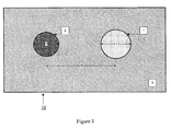
- FIG. 1 shows a scheme of a nanolaser according to a special embodiment of the present invention.
- Said nanolaser 10 for generating coherent electromagnetic radiation comprises a single nanoparticle 1 of metal, preferably silver, or semiconductor and a single exciting element 2 in the form of a quantum dot for exciting plasmon resonance of the nanoparticle 1.
- the exciting element 2 works as a pumping mechanism situated close to the nanoparticle 1.
- the whole system is embedded within a matrix 3 of Polaritonic or Photonic Band Gap (PGB)-material, e. g. Silica Carbide.
- PGB Polaritonic or Photonic Band Gap
- the nanoparticle 1 has a diameter r 1 and the exciting element 2 has a diameter r 2 .
- the distance between the nanoparticle 1 and the exciting element 2 is R.
- the exciting element 2 is pumped by a suitable pumping means (not shown). Said pumping means can work optically, electrically or chemically etc. Further, the exciting element 2 is coupled to the nanoparticle 1 to excite its plasmon modes. The excited plasmon modes, when de-excited, emit photons having certain spectral width.
- the usage of the PBG-material has the effect of reducing the spectral width of the emitted light of the nanolaser (system) much below that emitted by the exciting element 2 and the nanoparticle 1 when embedded within non-PBG-materials.
- the exciting element 2 is suitably tuned to excite the plasmon modes of the nanoparticle 1. It can come in any shape, configuration and material. Its sole role is to provide suitable excitation to the nanoparticle 1.
- the nanoparticle 1 has one or several plasmon resonances. It will absorb the energy coming out of the exciting element 2 and turns it into streams of photons.
- the nanoparticle 1 can have any shape or size that makes it suitable to the desired operation.
- the nanoparticle 1 and the exciting element 2 are shown as spherical, this is not necessary. They can take any shape for getting the desired results.
- the nanoparticle I can have a non-isomorphic shape that can support multiple plasmon resonances. Thus, by tuning the exciting element 2 to these resonances, photons with different colors can be generated.
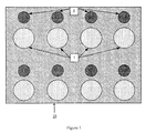
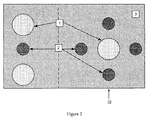
- the invention is not restricted to a single system. An ensemble of the system is also possible (see figures 2 and 3 and the description below).
- the nanolaser 10 can for example have the following dimensions:
- the PBG-material is Silica Carbide (SiC) and the nanoparticle 1 consists of silver or gold.
- the nanoparticles can range from a few nanometers to thousands of them.
- the exciting element size depends on its configuration. Quantum dots can be as small as a few nanometers across. Nevertheless, the smaller the nanolaser (system), the better,
- the nanoparticle 1 and the exciting element 2 should not be to close for the quadrupole moments to have a great effect on the nanolaser (system) and also should not be too far such that the nanoparticle 1 and the exciting element 2 can not interact through their near field dipole-dipole interaction.
- R should be equal or less than 26 nm.
- R should be a little bit smaller than that.
- 20 nm is a good value.
- the actual experimental values can be a bit different.
- the frequency of the system this depends on the plasmon resonance of the material of the nanoparticle.
- the plasmon resonance of bulk silver is around 5 x 10 15 Hz.
- ⁇ 1 and ⁇ 1 are the real values of the dielectric constant of silver and the surrounding medium (PBG). So for a nanoparticle of silver with a radius of 7 nm the value will be around 1.2221x10 15 Hz.
- Each material has its own distinctive plasmon resonance depending on the material of the surrounding matrix.
- the spectral width depends directly on this value. It also depends on the value of the pumping. The more the pumping, the narrower the spectral width and vice versa.
- the range of the spectral width depends on the range of the pumping, which depends on technical and industrial issues.
- the range of the spectral width of the light coming out of a silver nanoparticle embedded within Silica Carbide matrix is predicted to be around 1x10 13 to 1x10 10 Hz, respectively.
- Figure 2 shows an ensemble of spherical nanoparticles 1 (only some of them are indicated) and several exciting elements 2 (only some of them are indicated) in the form of quantum dots in a nanolaser according to another special embodiment of the invention.
- exciting elements 2 could be arranged within a layer or large slab of PBG-material as the matrix 3. Next one can embed many nanoparticles 1 below this layer of exciting elements 2. Whether there will be cross interaction between adjacent elements or not depends on the will of the experimenter and how careful he is in placing in these elements next to each other.
- a single exciting element 2 exciting two nanoparticles 1 is shown, whereas on the right side of said figure, four exciting elements 2 exciting one nanoparticle 1 are shown. So it is shown that an ensemble of several nanoparticles 1 and several exciting elements 2 can be used well.
Landscapes
- Physics & Mathematics (AREA)
- Optics & Photonics (AREA)
- Electromagnetism (AREA)
- Engineering & Computer Science (AREA)
- Condensed Matter Physics & Semiconductors (AREA)
- General Physics & Mathematics (AREA)
- Nanotechnology (AREA)
- Chemical & Material Sciences (AREA)
- Biophysics (AREA)
- Crystallography & Structural Chemistry (AREA)
- Life Sciences & Earth Sciences (AREA)
- Plasma & Fusion (AREA)
- Luminescent Compositions (AREA)
- Physical Or Chemical Processes And Apparatus (AREA)
Claims (8)
- Nanolaser (10) destiné à générer un rayonnement électromagnétique cohérent, comprenant :au moins une nanoparticule (1) de métal, de préférence argent ou or, ou semi-conductrice,au moins un élément d'excitation (2), de préférence un point quantique, pour exciter la résonance plasmonique de l'au moins une nanoparticule (1),dans lequel l'au moins une nanoparticule (1) et l'au moins un élément d'excitation (2) sont incorporés dans une matrice (3) de matériau à Bande interdite Photonique ou Polaritonique (PGB), de préférence du Carbure de Silicium (SiC).
- Nanolaser (10) selon la revendication 1, dans lequel l'au moins un élément d'excitation (2) présente deux niveaux d'énergie active.
- Nanolaser (10) selon la revendication 1 ou 2, comprenant en outre un moyen de pompage pour pomper l'au moins un élément d'excitation (2).
- Nanolaser (10) selon l'une quelconque des revendications 1 à 3, comprenant uniquement une seule nanoparticule (1) de métal ou semi-conductrice et uniquement un seul élément d'excitation (2).
- Nanolaser (10) selon la revendication 4, dans lequel la nanoparticule (1) est sphérique et a un diamètre r1, l'élément d'excitation (2) est sphérique et a un diamètre r2 et de préférence la distance R entre la nanoparticule (1) et l'élément d'excitation (2) est comme suit :

- Nanolaser (10) selon l'une quelconque des revendications 1 à 3, comprenant au moins deux nanoparticules (1) de métal ou semi-conductrices et uniquement un seul élément d'excitation (2).
- Nanolaser (10) selon l'une quelconque des revendications 1 à 3, comprenant uniquement une seule nanoparticule (1) de métal ou semi-conductrice et au moins deux éléments d'excitation (2).
- Nanolaser (10) selon l'une quelconque des revendications 1 à 3, comprenant au moins deux nanoparticules (1) de métal ou semi-conductrices et au moins deux éléments d'excitation (2), de préférence dans lequel les nanoparticules (1) sont agencées dans une couche ou des couches et/ou les éléments d'excitation (2) sont agencés dans une couche ou des couches.
Priority Applications (3)
| Application Number | Priority Date | Filing Date | Title |
|---|---|---|---|
| EP11196020.9A EP2610980B1 (fr) | 2011-12-29 | 2011-12-29 | Nano-laser pour générer un rayonnement électromagnétique cohérent |
| SA112340112A SA112340112B1 (ar) | 2011-12-29 | 2012-12-19 | أشعة ليزر نانونية لتوليد إشعاع كهرومغناطيسي مترابط |
| US13/719,322 US8971373B2 (en) | 2011-12-29 | 2012-12-19 | Nanolaser for generating coherent electromagnetic radiation |
Applications Claiming Priority (1)
| Application Number | Priority Date | Filing Date | Title |
|---|---|---|---|
| EP11196020.9A EP2610980B1 (fr) | 2011-12-29 | 2011-12-29 | Nano-laser pour générer un rayonnement électromagnétique cohérent |
Publications (2)
| Publication Number | Publication Date |
|---|---|
| EP2610980A1 EP2610980A1 (fr) | 2013-07-03 |
| EP2610980B1 true EP2610980B1 (fr) | 2014-02-12 |
Family
ID=45607546
Family Applications (1)
| Application Number | Title | Priority Date | Filing Date |
|---|---|---|---|
| EP11196020.9A Not-in-force EP2610980B1 (fr) | 2011-12-29 | 2011-12-29 | Nano-laser pour générer un rayonnement électromagnétique cohérent |
Country Status (3)
| Country | Link |
|---|---|
| US (1) | US8971373B2 (fr) |
| EP (1) | EP2610980B1 (fr) |
| SA (1) | SA112340112B1 (fr) |
Families Citing this family (3)
| Publication number | Priority date | Publication date | Assignee | Title |
|---|---|---|---|---|
| EP2781909B1 (fr) * | 2013-03-19 | 2021-09-29 | King Saud University | Nanostructures à base de plasmons de surface aptes à être utilisés comme nanocapteurs pour détecter des agents chimiques ou biologiques et systèmes pour la détection d'agents chimiques ou biologiques |
| RU2569050C2 (ru) * | 2013-12-10 | 2015-11-20 | Общество с ограниченной ответственностью "Гарант" (ООО "Гарант") | Решетка дипольных нанолазеров |
| US9500772B2 (en) * | 2014-12-11 | 2016-11-22 | The United States Of America As Represented By The Secretary Of The Navy | Metafilm for loss-induced super-scattering and gain-induced absorption of electromagnetic wave |
Family Cites Families (3)
| Publication number | Priority date | Publication date | Assignee | Title |
|---|---|---|---|---|
| WO2004100327A2 (fr) * | 2003-03-05 | 2004-11-18 | California Institute Of Technology | Sources de laser a cristaux photoniques pour detection chimique |
| RU2249278C2 (ru) | 2003-04-21 | 2005-03-27 | Займидорога Олег Антонович | Способ генерации когерентного электромагнитного излучения и дипольный нанолазер на его основе |
| US7400665B2 (en) * | 2004-11-05 | 2008-07-15 | Hewlett-Packard Developement Company, L.P. | Nano-VCSEL device and fabrication thereof using nano-colonnades |
-
2011
- 2011-12-29 EP EP11196020.9A patent/EP2610980B1/fr not_active Not-in-force
-
2012
- 2012-12-19 US US13/719,322 patent/US8971373B2/en not_active Expired - Fee Related
- 2012-12-19 SA SA112340112A patent/SA112340112B1/ar unknown
Also Published As
| Publication number | Publication date |
|---|---|
| EP2610980A1 (fr) | 2013-07-03 |
| US20130272335A1 (en) | 2013-10-17 |
| SA112340112B1 (ar) | 2015-07-07 |
| US20140064319A2 (en) | 2014-03-06 |
| US8971373B2 (en) | 2015-03-03 |
Similar Documents
| Publication | Publication Date | Title |
|---|---|---|
| Ma et al. | Multiplexed and electrically modulated plasmon laser circuit | |
| Azzam et al. | Ten years of spasers and plasmonic nanolasers | |
| Hsieh et al. | Perovskite quantum dot lasing in a gap-plasmon nanocavity with ultralow threshold | |
| Fernández-Domínguez et al. | Plasmon-enhanced generation of nonclassical light | |
| Ross et al. | Optical properties of one-, two-, and three-dimensional arrays of plasmonic nanostructures | |
| Negro et al. | Electromagnetic coupling and plasmon localization in deterministic aperiodic arrays | |
| US6999669B2 (en) | Photonic crystals | |
| US7560707B2 (en) | Apparatuses and methods for up-converting electromagnetic radiation | |
| Li et al. | Tunable open‐access microcavities for solid‐state quantum photonics and polaritonics | |
| EP2610980B1 (fr) | Nano-laser pour générer un rayonnement électromagnétique cohérent | |
| Abudayyeh et al. | Quantum emitters coupled to circular nanoantennas for high-brightness quantum light sources | |
| JP6479067B2 (ja) | 量子光学システム | |
| Kounoike et al. | Investigation of spontaneous emission from quantum dots embedded in two-dimensional photonic-crystal slab | |
| US7649679B2 (en) | Photon pair generating device | |
| Pan et al. | Angularly anisotropic tunability of upconversion luminescence by tuning plasmonic local-field responses in gold nanorods antennae with different configurations | |
| Wang et al. | Miniaturized optics from structured nanoscale cavities | |
| Sharma et al. | Ultrafast carrier dynamics in plasmonic-enhanced perovskite thin films for next-gen solar-powered wearables | |
| US6836494B1 (en) | Structure and method for processing optical energy | |
| Pellegrini et al. | Tunable, directional and wavelength selective plasmonic nanoantenna arrays | |
| EP1729383A1 (fr) | Source à Photon unique | |
| Keitel et al. | Active mode switching in plasmonic microlasers by spatial control of optical gain | |
| JP2006060143A (ja) | 光ファイバ型単一光子発生素子および単一光子発生装置 | |
| EP4077209B1 (fr) | Dispositif optique à photon unique | |
| US20090321712A1 (en) | Plasmonic coupling devices | |
| KR20220026199A (ko) | 단일 양자 광원 유도 및 조절 시스템 및 단일 양자 광원 유도 및 조절 방법 |
Legal Events
| Date | Code | Title | Description |
|---|---|---|---|
| PUAI | Public reference made under article 153(3) epc to a published international application that has entered the european phase |
Free format text: ORIGINAL CODE: 0009012 |
|
| AK | Designated contracting states |
Kind code of ref document: A1 Designated state(s): AL AT BE BG CH CY CZ DE DK EE ES FI FR GB GR HR HU IE IS IT LI LT LU LV MC MK MT NL NO PL PT RO RS SE SI SK SM TR |
|
| AX | Request for extension of the european patent |
Extension state: BA ME |
|
| 17P | Request for examination filed |
Effective date: 20130617 |
|
| RBV | Designated contracting states (corrected) |
Designated state(s): AL AT BE BG CH CY CZ DE DK EE ES FI FR GB GR HR HU IE IS IT LI LT LU LV MC MK MT NL NO PL PT RO RS SE SI SK SM TR |
|
| GRAP | Despatch of communication of intention to grant a patent |
Free format text: ORIGINAL CODE: EPIDOSNIGR1 |
|
| INTG | Intention to grant announced |
Effective date: 20131007 |
|
| RIN1 | Information on inventor provided before grant (corrected) |
Inventor name: GHANNAM, TALAL |
|
| GRAS | Grant fee paid |
Free format text: ORIGINAL CODE: EPIDOSNIGR3 |
|
| GRAA | (expected) grant |
Free format text: ORIGINAL CODE: 0009210 |
|
| AK | Designated contracting states |
Kind code of ref document: B1 Designated state(s): AL AT BE BG CH CY CZ DE DK EE ES FI FR GB GR HR HU IE IS IT LI LT LU LV MC MK MT NL NO PL PT RO RS SE SI SK SM TR |
|
| REG | Reference to a national code |
Ref country code: GB Ref legal event code: FG4D |
|
| REG | Reference to a national code |
Ref country code: CH Ref legal event code: EP |
|
| REG | Reference to a national code |
Ref country code: AT Ref legal event code: REF Ref document number: 652495 Country of ref document: AT Kind code of ref document: T Effective date: 20140215 |
|
| REG | Reference to a national code |
Ref country code: IE Ref legal event code: FG4D |
|
| REG | Reference to a national code |
Ref country code: DE Ref legal event code: R096 Ref document number: 602011004932 Country of ref document: DE Effective date: 20140327 |
|
| REG | Reference to a national code |
Ref country code: NL Ref legal event code: VDEP Effective date: 20140212 |
|
| REG | Reference to a national code |
Ref country code: AT Ref legal event code: MK05 Ref document number: 652495 Country of ref document: AT Kind code of ref document: T Effective date: 20140212 |
|
| REG | Reference to a national code |
Ref country code: LT Ref legal event code: MG4D |
|
| PG25 | Lapsed in a contracting state [announced via postgrant information from national office to epo] |
Ref country code: NO Free format text: LAPSE BECAUSE OF FAILURE TO SUBMIT A TRANSLATION OF THE DESCRIPTION OR TO PAY THE FEE WITHIN THE PRESCRIBED TIME-LIMIT Effective date: 20140512 Ref country code: LT Free format text: LAPSE BECAUSE OF FAILURE TO SUBMIT A TRANSLATION OF THE DESCRIPTION OR TO PAY THE FEE WITHIN THE PRESCRIBED TIME-LIMIT Effective date: 20140212 Ref country code: IS Free format text: LAPSE BECAUSE OF FAILURE TO SUBMIT A TRANSLATION OF THE DESCRIPTION OR TO PAY THE FEE WITHIN THE PRESCRIBED TIME-LIMIT Effective date: 20140612 |
|
| PG25 | Lapsed in a contracting state [announced via postgrant information from national office to epo] |
Ref country code: PT Free format text: LAPSE BECAUSE OF FAILURE TO SUBMIT A TRANSLATION OF THE DESCRIPTION OR TO PAY THE FEE WITHIN THE PRESCRIBED TIME-LIMIT Effective date: 20140612 Ref country code: CY Free format text: LAPSE BECAUSE OF FAILURE TO SUBMIT A TRANSLATION OF THE DESCRIPTION OR TO PAY THE FEE WITHIN THE PRESCRIBED TIME-LIMIT Effective date: 20140212 Ref country code: FI Free format text: LAPSE BECAUSE OF FAILURE TO SUBMIT A TRANSLATION OF THE DESCRIPTION OR TO PAY THE FEE WITHIN THE PRESCRIBED TIME-LIMIT Effective date: 20140212 Ref country code: AT Free format text: LAPSE BECAUSE OF FAILURE TO SUBMIT A TRANSLATION OF THE DESCRIPTION OR TO PAY THE FEE WITHIN THE PRESCRIBED TIME-LIMIT Effective date: 20140212 Ref country code: NL Free format text: LAPSE BECAUSE OF FAILURE TO SUBMIT A TRANSLATION OF THE DESCRIPTION OR TO PAY THE FEE WITHIN THE PRESCRIBED TIME-LIMIT Effective date: 20140212 Ref country code: SE Free format text: LAPSE BECAUSE OF FAILURE TO SUBMIT A TRANSLATION OF THE DESCRIPTION OR TO PAY THE FEE WITHIN THE PRESCRIBED TIME-LIMIT Effective date: 20140212 Ref country code: ES Free format text: LAPSE BECAUSE OF FAILURE TO SUBMIT A TRANSLATION OF THE DESCRIPTION OR TO PAY THE FEE WITHIN THE PRESCRIBED TIME-LIMIT Effective date: 20140212 |
|
| PG25 | Lapsed in a contracting state [announced via postgrant information from national office to epo] |
Ref country code: HR Free format text: LAPSE BECAUSE OF FAILURE TO SUBMIT A TRANSLATION OF THE DESCRIPTION OR TO PAY THE FEE WITHIN THE PRESCRIBED TIME-LIMIT Effective date: 20140212 Ref country code: BE Free format text: LAPSE BECAUSE OF FAILURE TO SUBMIT A TRANSLATION OF THE DESCRIPTION OR TO PAY THE FEE WITHIN THE PRESCRIBED TIME-LIMIT Effective date: 20140212 Ref country code: RS Free format text: LAPSE BECAUSE OF FAILURE TO SUBMIT A TRANSLATION OF THE DESCRIPTION OR TO PAY THE FEE WITHIN THE PRESCRIBED TIME-LIMIT Effective date: 20140212 Ref country code: LV Free format text: LAPSE BECAUSE OF FAILURE TO SUBMIT A TRANSLATION OF THE DESCRIPTION OR TO PAY THE FEE WITHIN THE PRESCRIBED TIME-LIMIT Effective date: 20140212 |
|
| PG25 | Lapsed in a contracting state [announced via postgrant information from national office to epo] |
Ref country code: EE Free format text: LAPSE BECAUSE OF FAILURE TO SUBMIT A TRANSLATION OF THE DESCRIPTION OR TO PAY THE FEE WITHIN THE PRESCRIBED TIME-LIMIT Effective date: 20140212 Ref country code: RO Free format text: LAPSE BECAUSE OF FAILURE TO SUBMIT A TRANSLATION OF THE DESCRIPTION OR TO PAY THE FEE WITHIN THE PRESCRIBED TIME-LIMIT Effective date: 20140212 Ref country code: CZ Free format text: LAPSE BECAUSE OF FAILURE TO SUBMIT A TRANSLATION OF THE DESCRIPTION OR TO PAY THE FEE WITHIN THE PRESCRIBED TIME-LIMIT Effective date: 20140212 Ref country code: DK Free format text: LAPSE BECAUSE OF FAILURE TO SUBMIT A TRANSLATION OF THE DESCRIPTION OR TO PAY THE FEE WITHIN THE PRESCRIBED TIME-LIMIT Effective date: 20140212 |
|
| REG | Reference to a national code |
Ref country code: DE Ref legal event code: R097 Ref document number: 602011004932 Country of ref document: DE |
|
| PG25 | Lapsed in a contracting state [announced via postgrant information from national office to epo] |
Ref country code: SK Free format text: LAPSE BECAUSE OF FAILURE TO SUBMIT A TRANSLATION OF THE DESCRIPTION OR TO PAY THE FEE WITHIN THE PRESCRIBED TIME-LIMIT Effective date: 20140212 Ref country code: PL Free format text: LAPSE BECAUSE OF FAILURE TO SUBMIT A TRANSLATION OF THE DESCRIPTION OR TO PAY THE FEE WITHIN THE PRESCRIBED TIME-LIMIT Effective date: 20140212 |
|
| PLBE | No opposition filed within time limit |
Free format text: ORIGINAL CODE: 0009261 |
|
| STAA | Information on the status of an ep patent application or granted ep patent |
Free format text: STATUS: NO OPPOSITION FILED WITHIN TIME LIMIT |
|
| 26N | No opposition filed |
Effective date: 20141113 |
|
| REG | Reference to a national code |
Ref country code: DE Ref legal event code: R097 Ref document number: 602011004932 Country of ref document: DE Effective date: 20141113 |
|
| PG25 | Lapsed in a contracting state [announced via postgrant information from national office to epo] |
Ref country code: IT Free format text: LAPSE BECAUSE OF FAILURE TO SUBMIT A TRANSLATION OF THE DESCRIPTION OR TO PAY THE FEE WITHIN THE PRESCRIBED TIME-LIMIT Effective date: 20140212 |
|
| PG25 | Lapsed in a contracting state [announced via postgrant information from national office to epo] |
Ref country code: SI Free format text: LAPSE BECAUSE OF FAILURE TO SUBMIT A TRANSLATION OF THE DESCRIPTION OR TO PAY THE FEE WITHIN THE PRESCRIBED TIME-LIMIT Effective date: 20140212 |
|
| PG25 | Lapsed in a contracting state [announced via postgrant information from national office to epo] |
Ref country code: LU Free format text: LAPSE BECAUSE OF FAILURE TO SUBMIT A TRANSLATION OF THE DESCRIPTION OR TO PAY THE FEE WITHIN THE PRESCRIBED TIME-LIMIT Effective date: 20141229 |
|
| REG | Reference to a national code |
Ref country code: CH Ref legal event code: PL |
|
| REG | Reference to a national code |
Ref country code: IE Ref legal event code: MM4A |
|
| PG25 | Lapsed in a contracting state [announced via postgrant information from national office to epo] |
Ref country code: CH Free format text: LAPSE BECAUSE OF NON-PAYMENT OF DUE FEES Effective date: 20141231 Ref country code: LI Free format text: LAPSE BECAUSE OF NON-PAYMENT OF DUE FEES Effective date: 20141231 Ref country code: IE Free format text: LAPSE BECAUSE OF NON-PAYMENT OF DUE FEES Effective date: 20141229 |
|
| REG | Reference to a national code |
Ref country code: FR Ref legal event code: PLFP Year of fee payment: 5 |
|
| PG25 | Lapsed in a contracting state [announced via postgrant information from national office to epo] |
Ref country code: SM Free format text: LAPSE BECAUSE OF FAILURE TO SUBMIT A TRANSLATION OF THE DESCRIPTION OR TO PAY THE FEE WITHIN THE PRESCRIBED TIME-LIMIT Effective date: 20140212 |
|
| PG25 | Lapsed in a contracting state [announced via postgrant information from national office to epo] |
Ref country code: MC Free format text: LAPSE BECAUSE OF FAILURE TO SUBMIT A TRANSLATION OF THE DESCRIPTION OR TO PAY THE FEE WITHIN THE PRESCRIBED TIME-LIMIT Effective date: 20140212 |
|
| PG25 | Lapsed in a contracting state [announced via postgrant information from national office to epo] |
Ref country code: BG Free format text: LAPSE BECAUSE OF FAILURE TO SUBMIT A TRANSLATION OF THE DESCRIPTION OR TO PAY THE FEE WITHIN THE PRESCRIBED TIME-LIMIT Effective date: 20140212 Ref country code: GR Free format text: LAPSE BECAUSE OF FAILURE TO SUBMIT A TRANSLATION OF THE DESCRIPTION OR TO PAY THE FEE WITHIN THE PRESCRIBED TIME-LIMIT Effective date: 20140513 |
|
| PG25 | Lapsed in a contracting state [announced via postgrant information from national office to epo] |
Ref country code: HU Free format text: LAPSE BECAUSE OF FAILURE TO SUBMIT A TRANSLATION OF THE DESCRIPTION OR TO PAY THE FEE WITHIN THE PRESCRIBED TIME-LIMIT; INVALID AB INITIO Effective date: 20111229 Ref country code: MT Free format text: LAPSE BECAUSE OF FAILURE TO SUBMIT A TRANSLATION OF THE DESCRIPTION OR TO PAY THE FEE WITHIN THE PRESCRIBED TIME-LIMIT Effective date: 20140212 Ref country code: TR Free format text: LAPSE BECAUSE OF FAILURE TO SUBMIT A TRANSLATION OF THE DESCRIPTION OR TO PAY THE FEE WITHIN THE PRESCRIBED TIME-LIMIT Effective date: 20140212 |
|
| REG | Reference to a national code |
Ref country code: FR Ref legal event code: PLFP Year of fee payment: 6 |
|
| REG | Reference to a national code |
Ref country code: FR Ref legal event code: PLFP Year of fee payment: 7 |
|
| PG25 | Lapsed in a contracting state [announced via postgrant information from national office to epo] |
Ref country code: MK Free format text: LAPSE BECAUSE OF FAILURE TO SUBMIT A TRANSLATION OF THE DESCRIPTION OR TO PAY THE FEE WITHIN THE PRESCRIBED TIME-LIMIT Effective date: 20140212 |
|
| PG25 | Lapsed in a contracting state [announced via postgrant information from national office to epo] |
Ref country code: AL Free format text: LAPSE BECAUSE OF FAILURE TO SUBMIT A TRANSLATION OF THE DESCRIPTION OR TO PAY THE FEE WITHIN THE PRESCRIBED TIME-LIMIT Effective date: 20140212 |
|
| PGFP | Annual fee paid to national office [announced via postgrant information from national office to epo] |
Ref country code: DE Payment date: 20190329 Year of fee payment: 8 Ref country code: FR Payment date: 20190329 Year of fee payment: 8 |
|
| PGFP | Annual fee paid to national office [announced via postgrant information from national office to epo] |
Ref country code: GB Payment date: 20190424 Year of fee payment: 8 |
|
| REG | Reference to a national code |
Ref country code: DE Ref legal event code: R119 Ref document number: 602011004932 Country of ref document: DE |
|
| GBPC | Gb: european patent ceased through non-payment of renewal fee |
Effective date: 20191229 |
|
| PG25 | Lapsed in a contracting state [announced via postgrant information from national office to epo] |
Ref country code: FR Free format text: LAPSE BECAUSE OF NON-PAYMENT OF DUE FEES Effective date: 20191231 Ref country code: DE Free format text: LAPSE BECAUSE OF NON-PAYMENT OF DUE FEES Effective date: 20200701 Ref country code: GB Free format text: LAPSE BECAUSE OF NON-PAYMENT OF DUE FEES Effective date: 20191229 |