EP2612492B1 - Capteur d'images à plage dynamique étendue - Google Patents
Capteur d'images à plage dynamique étendue Download PDFInfo
- Publication number
- EP2612492B1 EP2612492B1 EP11760911.5A EP11760911A EP2612492B1 EP 2612492 B1 EP2612492 B1 EP 2612492B1 EP 11760911 A EP11760911 A EP 11760911A EP 2612492 B1 EP2612492 B1 EP 2612492B1
- Authority
- EP
- European Patent Office
- Prior art keywords
- sample
- time
- pixel cell
- cell signal
- exposure time
- Prior art date
- Legal status (The legal status is an assumption and is not a legal conclusion. Google has not performed a legal analysis and makes no representation as to the accuracy of the status listed.)
- Not-in-force
Links
Images




Classifications
-
- H—ELECTRICITY
- H04—ELECTRIC COMMUNICATION TECHNIQUE
- H04N—PICTORIAL COMMUNICATION, e.g. TELEVISION
- H04N25/00—Circuitry of solid-state image sensors [SSIS]; Control thereof
- H04N25/50—Control of the SSIS exposure
- H04N25/57—Control of the dynamic range
-
- H—ELECTRICITY
- H04—ELECTRIC COMMUNICATION TECHNIQUE
- H04N—PICTORIAL COMMUNICATION, e.g. TELEVISION
- H04N25/00—Circuitry of solid-state image sensors [SSIS]; Control thereof
- H04N25/50—Control of the SSIS exposure
- H04N25/57—Control of the dynamic range
- H04N25/58—Control of the dynamic range involving two or more exposures
- H04N25/587—Control of the dynamic range involving two or more exposures acquired sequentially, e.g. using the combination of odd and even image fields
- H04N25/589—Control of the dynamic range involving two or more exposures acquired sequentially, e.g. using the combination of odd and even image fields with different integration times, e.g. short and long exposures
-
- H—ELECTRICITY
- H04—ELECTRIC COMMUNICATION TECHNIQUE
- H04N—PICTORIAL COMMUNICATION, e.g. TELEVISION
- H04N25/00—Circuitry of solid-state image sensors [SSIS]; Control thereof
- H04N25/70—SSIS architectures; Circuits associated therewith
- H04N25/76—Addressed sensors, e.g. MOS or CMOS sensors
- H04N25/77—Pixel circuitry, e.g. memories, A/D converters, pixel amplifiers, shared circuits or shared components
Definitions
- the disclosure relates to image sensors and, in particular, techniques for producing high dynamic range images.
- the dynamic range of a scene is determined by a ratio of the highest and lowest light levels of the scene.
- the dynamic range of a sensor is determined by a ratio of the highest light level in a scene that does not saturate the sensor to the lowest light level, i.e., above a noise floor, detectable by the sensor.
- the dynamic range of a scene may be, for example, 100,000:1, while the dynamic range of a sensor may be, for example, 100:1.
- Exposure may be adjusted in a manner such that the dynamic range of a sensor covers as much useful light level as possible. Exposure cannot increase the dynamic range of the sensor. However, combining two or more different exposures of a scene may permit the capture of a higher dynamic range of the scene then would otherwise be possible by a single exposure.
- Some techniques provide software solutions that align two images of different exposure times in order to form a higher dynamic range image than would otherwise be possible.
- Other techniques provide hardware solutions, e.g., modified sensors, to capture two images of a scene that will be aligned to form a higher dynamic range image.
- US 2007/0268396 A1 describes an image pickup device in which standard image signals and non-standard image signals with a smaller exposure value are obtained. Saturation determination signals are generated and pixels which are predicted to be saturated during the standard exposure time being the normalized short exposure pixel data is outputted while for pixels which are predicted not to be saturated during the standard exposure time the standard exposure pixel data is outputted.
- this disclosure describes techniques for producing high dynamic range images by applying a variable weighting factor to a sample prior to combining the sample with another sample.
- An image sensor may sample a pixel cell signal at two or more different exposure times in order to produce two or more samples that may be combined to produce a high dynamic range image.
- a long exposure time may cause a photosensitive semiconductor of the pixel cell to become saturated.
- a variable weighting factor may be applied to the signal produced by the long exposure time in order to reduce or eliminate the contribution of the saturated photosensitive semiconductor.
- the disclosure is directed to a method according to claim 1.
- the disclosure is directed to a system according to claim 9.
- HDR high dynamic range
- a HDR image refers to an image that has a dynamic range, e.g., a ratio of the highest intensity light level relative to the lowest intensity light level in the image, greater than that of image produced by standard imaging techniques.
- One example HDR imaging technique combines images captured with different exposure times to create a combined image with a greater dynamic range then that of an image produced from either of the exposure times.
- This disclosure provides techniques that apply a variable weighting factor to one of the images captured with different exposure times prior to combining the images in order to produce a HDR image.
- FIG. 1 is a schematic diagram of an example picture element ("pixel") cell that may be used to implement the techniques of this disclosure.
- example pixel cell 10 comprises photosensitive semiconductor 12, switches 14, 16, and 18, capacitor 20, and transistors 22, 24. Switches 14, 16, and 18 may be transistors, for example.
- a capacitance is associated with photosensitive semiconductor 12, as indicated by equivalent capacitor 28 (shown by dashed lines).
- the cathode of photosensitive semiconductor 12 is connected to voltage source V DD through switch 14, and the anode of photosensitive semiconductor 12 is connected to reference voltage V SS , which may be ground or other potential less than voltage source V DD .
- V SS reference voltage
- photosensitive semiconductor 12 is reverse-biased because its cathode at node 30 is at a higher potential than its anode.
- the gate of transistor 22 is connected to the cathode of photosensitive semiconductor 12 through switch 16.
- the gate of transistor 22 is also connected to capacitor 20 through switch 18.
- the drain of transistor 22 is connector to voltage source V DD , and the source of transistor 22 is connected to the drain of transistor 24.
- Gate 26 of transistor 24 is connected to row select driver circuitry, as described in more detail below.
- the source of transistor 24 is connector to pixel cell output line 32.
- transistors 22 and 24 are depicted as enhancement-mode metal-oxide-semiconductor field-effect transistors (MOSFETs) without their respective bulks attached, numerous other configurations are possible.
- transistors 22 and 24 are described below as n-MOS type transistors, in other example configurations, transistors 22 and 24 may be p-MOS type transistors.
- Photosensitive semiconductor 12 e.g., a photodiode
- Photosensitive semiconductor 12 is a device that converts photons from incident light into electrical charge.
- photons from the incident light cause the photosensitive semiconductor to generate charge carriers within a region of the photosensitive semiconductor.
- the amount of charge carriers generated is proportional to the amount of incident light. As light intensity increases, the amount of charge carriers generated increases.
- the photosensitive semiconductor may become "saturated" if the amount of charge carriers can no longer increase as the amount of incident light increases. It should be appreciated that once a photosensitive semiconductor becomes saturated, it is no longer an accurate indicator of the amount of incident light. As such, the saturated photosensitive semiconductor has little information of value.
- photosensitive semiconductor 12 e.g., a photodiode
- photosensitive semiconductor 12 Prior to exposure to light, pixel cell 10 may be reset to an initial voltage.
- photosensitive semiconductor 12 and its equivalent capacitance 28 may be reset to an initial voltage of V DD , for example.
- reset switch 14 may be closed in order to reset pixel cell 10 of FIG. 1 . Closing reset switch 14 connects node 30 and, in particular, photosensitive semiconductor 12 and its equivalent capacitor 28, to supply voltage V DD .
- pixel cell 10 may include a second voltage, similar to or different from supply voltage V DD that acts as a dedicated reset voltage for pixel cell 10.
- Closing reset switch 14 drains charge out of photosensitive semiconductor 12 and charges equivalent capacitor 28 to known voltage V DD .
- switches 16 and 18 are closed at reset, which can cause capacitor 20 to become charged to known voltage V DD .
- photosensitive semiconductor 12 begins converting photons to charge upon exposure to light,.
- photosensitive semiconductor 12 Upon exposure to light, i.e., at the beginning of its integration time, photosensitive semiconductor 12 begins generating charge carriers. Because photosensitive semiconductor 12 is reverse-biased, photocurrent will begin to flow from the cathode to the anode of photosensitive semiconductor 12. The photocurrent is proportional to the amount of incident light. As light intensity increases, the amount of charge carriers generated by photosensitive semiconductor 12 increases, thereby increasing the photocurrent. The photocurrent begins to discharge equivalent capacitor 28.
- Pixel cell 10 may be used to sample a first pixel cell signal at a first time, e.g., a short exposure time, and a second pixel cell signal at a second time, e.g., a long exposure time.
- pixel cell 10 may sample a first signal from photosensitive semiconductor 12 by closing switches 16 and 18.
- a controller e.g., controller 54 of FIG. 3
- a controller e.g., controller 54 of FIG. 3
- a long exposure time sample is represented by the voltage remaining on equivalent capacitor 28.
- the long exposure time sample may be read out by closing switch 16 and applying a row select signal to gate 26 of transistor 24 (described in more detail below).
- a controller e.g., controller 54 of FIG. 3 ) closes switch 16 and applies a row select signal to gate 26 of transistor 24 to turn on transistors 22 and 24.
- a voltage representing the long exposure time sample is then read out from pixel cell 10 and, in particular, equivalent capacitor 28, via line 32 through transistors 22 and 24.
- the short exposure time sample stored in capacitor 20 may be read out.
- the short exposure time sample may be read out by opening switch 16, closing switch 18, and applying a row select signal to gate 26 of transistor 24. Closing switch 18 and applying a row select signal to gate 26 of transistor 24 turns on transistors 22 and 24.
- the voltage stored on capacitor 30, which represents the short exposure time sample, is then read out from pixel cell 10 via line 32. The voltage that is read out is approximately equal to the voltage across capacitor 30 minus the threshold voltages of transistors 22 and 24.
- CMOS complementary MOS
- FPN fixed pattern noise
- a controller on the image sensor may perform correlated double sampling by closing switch 14, thereby resetting pixel cell 10 to reference voltage V DD , and then sampling the output level of the pixel cell after the pixel cell has been reset.
- the controller may reset, sample, and read out the reset value of a pixel cell, e.g. pixel cell 10. Then, the controller may subtract the pixel cell's reset value from the value of the signal sample in order to provide a more accurate representation of the signal.
- the short exposure time sample and the long exposure time sample may be combined by a processor after applying a variable weighting factor to the long exposure time sample.
- a variable weighting factor that is defined by a function at the value of the long exposure time sample, the dynamic range provided by the two different exposure times may be improved.
- the contribution of the long exposure time sample may be reduced or eliminated by the weighting factor during the combination of the short exposure time sample and the long exposure time sample.
- a photosensitive semiconductor becomes saturated, it is no longer an accurate indicator of the amount of incident light. As such, the saturated photosensitive semiconductor has little information of value.
- a pixel cell is unlikely to saturate. Hence, the short exposure time sample likely has more valuable information than the saturated, or overexposed, long exposure time sample.
- S COMBINED is the combination of the short exposure time sample S SHORT (i, j) and the long exposure time sample S LONG (i, j) for the pixel cell located at (i, j)
- C() is a combining curve that begins at a value of one and decreases to a value of zero as long exposure time sample S LONG (i, j) becomes saturated
- M(i, j) is a scalar value of the long exposure time sample S LONG (i, j) weighted by
- H(i, j) and V(i, j) are equal to zero and equation (2) above may be reduced to the following:
- S COMBINED i , j S LONG i , j * M i , j + n * S SHORT i , j * 1 ⁇ M i , j
- the long exposure time sample S LONG (i, j) in equations (2) and (3) may be modified by the scalar value n.
- the scalar value n may comprise the ratio of the short exposure time and the long exposure time.
- the scalar value n may be used in order to normalize the long exposure time sample S LONG (i, j) and the short exposure time sample S SHORT (i, j) by bringing the two samples to a common base.
- the combining scheme described by equations (2) and (3) adjusts the value n so that objects appear at the same level in both images prior to their combination.
- one half of a frame of a scene has a luminance value of 100 lux and the other half has a luminance value of 1000 lux.
- the frame has a luminance ratio of 10:1.
- S SHORT corresponds to the 1000 lux portion of the frame
- S LONG corresponds to the 100 lux portion of the frame
- the long exposure time T LONG equals one second
- the short exposure time T SHORT equals 0.1 seconds.
- the short exposure time sample of 1000 lux must be scaled downward to the long exposure time sample of 100 lux.
- a processor e.g., processor 76 of FIG. 3
- the "noise floor" of the pixel cell i.e., the low-level signal produced by pixel cells in the absence of incident light, is a factor in reducing dynamic range.
- the short exposure time sample S SHORT (i, j) and long exposure time sample S LONG (i, j) may be combined in a signal-to-noise (SNR) efficient manner. That is, if a sample has a value below the SNR of the pixel cell itself, the sample may be discarded.
- FIG. 2 is an example graph of a combining curve, namely C (), that may be used in a combining scheme in accordance with the techniques of this disclosure.
- the x-axis of the graph depicted in FIG. 2 represents the luma value of the pixel cell located at a spatial location (i, j) on the pixel cell array after a long exposure time.
- the y-axis of the graph depicted in FIG. 2 represents the weighted value, M(i, j), of S LONG (i, j) as defined by combining curve C(), shown generally at 40.
- the value of S LONG (i, j) is zero. If the pixel cell located at (i, j) is saturated after a long exposure time, then the value of S LONG (i, j) is at a maximum, e.g., 255 for an eight-bit implementation. As seen in FIG. 2 , as the value of S LONG (i, j) increases, the value of M(i, j) remains at a value of "1" until an S LONG (i, j) value of about 210.
- the combining curve C() begins to decrease sharply between the S LONG (i, j) values of about 210 and about 230 until the weighted value M(i, j) reaches a value of "0" at an S LONG (i, j) value of about 230. Between the S LONG (i, j) values of about 210 and about 230, the weighted value M(i, j) may be a value between "0" and "1.” For example, at an S LONG (i, j) value of about 220, the weighted value M(i, j) is about 0.5.
- the example combining curve C ( ), depicted at 40 in FIG. 2 includes three segments, 42, 44 and 46. In other examples, combining curve C () may have more, or fewer segments. As seen in FIG. 2 , combining curve C () may generally be considered a decaying function as the value of the long exposure time sample S LONG (i, j) increases. In other examples, combining curve C () may decay less sharply.
- the dynamic range of the sensor can be made variable and programmable. Every pixel cell may have a different weighted value M(i, j) that varies according to the value of the long exposure time sample value S LONG (i, j) for that particular pixel cell. Unlike other image sensors in which the dynamic range of the sensor is fixed based upon values of capacitors used to construct the sensor, using the techniques of this disclosure the dynamic range is adaptable, e.g., for a particular scene.
- f-stops are a measure of dynamic range for digital cameras
- the exposure times may be adjusted to provide four f-stops, and then the two samples from the two exposure times may be combined.
- a combining curve may be generated according to one or more of the following three guidelines.
- the combining curve may be image level dependent. Any of the two images may be used with comparable results but the two curves will differ.
- the combining curve may weight less noisy images more heavily than more noisy images. For example, the long exposure time sample, S LONG , which likely has less noise than short exposure time sample S SHORT (i, j), may be weighted more heavily than S SHORT . In some examples, however, equal gain combining may be used, rather than weighted one image more heavily than another.
- the combining curve may be monotonically decreasing.
- prior knowledge may be used to model noise statistics based on the image level and utilize maximum ratio combining where each image is scaled inversely proportional to its noise levels.
- an enhanced version of the first example methodology may be used for which the transition from 1 to 0 is made more gradual.
- L is the luma value associated with S LONG (i, j), e.g., a combination of R, G, B components like (R+G+B)/2, max(R,G,B), or the like and having a value of 0-255 in an 8-bit implementation
- the dynamic range of the imaging sensor may be reduced to improve the noise characteristics of the sensor. Collecting and combining two samples of approximately equal exposure times, i.e., T LONG is approximately equal to T SHORT , may reduce noise. When combined, the noise can be averaged between the two samples, and thus may be significantly reduced.
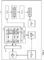
- FIG. 3 is a block diagram of an example image sensor that may be used to implement the techniques of this disclosure.
- image sensor 50 of FIG. 3 is a complementary MOS (CMOS) image sensor
- CMOS complementary MOS
- the signal combining techniques described in this disclosure are applicable to other image sensors as well, including, for example, charge-coupled device (CCD) image sensors.
- CCD charge-coupled device
- image sensor 50 includes pixel cell array 52 comprising numerous pixel cells 10.
- Pixel cell array 52 may be arranged in M rows and N columns of pixel cells 10, as shown in FIG. 3 .
- Each pixel cell 10 of pixel cell array 52 may be addressed by a row and column address.
- controller 54 provides row address decoder 56 with a digital address of the row of the desired pixel cell, e.g., row M.
- Row address decoder 56 decodes the received row address and outputs a "row select" signal to row driver 58 to apply a voltage to row M, thereby selecting each pixel cell 10 in row M, e.g., by applying a voltage on gate 26 of transistor 24 in FIG. 1 .
- Controller 54 also provides column address decoder 60 with a digital address of the column of the desired pixel cell, e.g., column N.
- Column address decoder 60 decodes the received column address and outputs a "column select” signal to column diver 62 to apply a voltage to column N, thereby selecting each pixel cell 10 in column N. In this manner, pixel cell 10 at row M, column N may be selected and its voltage read out.
- Controller 54 may include one or more microprocessors, digital signal processors (DSPs), application specific integrated circuits (ASICs), field programmable gate arrays (FPGAs), discrete logic, or other processor arrangements suitable for processing computer code to facilitate the execution of the functions described in this disclosure.
- DSPs digital signal processors
- ASICs application specific integrated circuits
- FPGAs field programmable gate arrays
- discrete logic or other processor arrangements suitable for processing computer code to facilitate the execution of the functions described in this disclosure.
- the voltage of pixel cell 10 at row M, column N is sampled and held by sample and hold (S/H) circuitry 70.
- S/H sample and hold
- Processing such as black level compensation, noise reduction, e.g., temporal noise and FPN, and amplification is performed on analog signals by processing circuitry 72.
- the analog signals from pixel cells 10 are quantized to digital values via analog-to-digital converter (ADC) 74.
- ADC analog-to-digital converter
- the digital values are then input into processor 76.
- Processor 76 may combine, for each pixel cell, the short exposure time sample S SHORT and the long exposure time sample S LONG , in accordance with the techniques described in this disclosure, with particular reference to equations (1)-(3) above.
- processor 76 may execute instructions in order to perform the functions described in this disclosure.
- the instructions may be stored in memory 78.
- Processor 76 may include one or more microprocessors, digital signal processors (DSPs), application specific integrated circuits (ASICs), field programmable gate arrays (FPGAs), discrete logic, or other processor arrangements suitable for processing computer code to facilitate the execution of the functions described in this disclosure.
- DSPs digital signal processors
- ASICs application specific integrated circuits
- FPGAs field programmable gate arrays
- discrete logic discrete logic
- the executable instructions stored in memory 78 may comprise computer-readable instructions encoded in a computer-readable medium such as random access memory (RAM), synchronous dynamic random access memory (SDRAM), read-only memory (ROM), non-volatile random access memory (NVRAM), electrically erasable programmable read-only memory (EEPROM), FLASH memory, magnetic or optical data storage media, and the like.
- RAM random access memory
- SDRAM synchronous dynamic random access memory
- ROM read-only memory
- NVRAM non-volatile random access memory
- EEPROM electrically erasable programmable read-only memory
- FLASH memory magnetic or optical data storage media, and the like.
- processor 76 receives the digitized pixel cell values for pixel cell 10 at row M, column N.
- processor 76 receives a digital value for long exposure time sample S LONG (m, n) and a digital value for short exposure time sample S SHORT (m, n) from pixel cell (m, n).
- processor 76 may combine long exposure time sample S LONG (m, n) and a digital value for short exposure time sample S SHORT (m, n) from pixel cell (m, n).
- Processor 76 may calculate, obtain, or otherwise acquire variable weighting factor M(m, n) for long exposure time sample S LONG (m, n), where M(m,n) is determined by evaluating C() at S LONG (m, n), or C(S LONG (m, n)).
- combining curve C( ) may be defined by one or more equations. Each equation defining a combining curve C () may, for example, be dependent upon the desired dynamic range, e.g., f-stop value. For example, a user may have selected a certain f-stop value to achieve a desired dynamic range, which in turn corresponds to a specific combining curve C () that may be retrieved from memory 78.
- processor 76 may determine the value of variable weighting factor M(m, n) by evaluating a particular equation that defines combining curve C (), e.g., retrieved from memory 78, for the desired dynamic range at the value of S LONG (m, n). For example, assume that the pixel cell 10 was saturated at long exposure time sample S LONG (m, n). Regardless of the number of bits in the implementation, if the combining curve depicted in FIG. 2 is used by processor 76, then the resulting variable weighting factor M(m, n) is zero.
- variable weighting factor M(m, n) is zero, as determined by evaluating combining curve C ( ), or an equation defining combining curve C ( ), at long exposure time sample, S LONG (m, n).
- the combined value S COMBINED is simply the value of the short exposure time sample, S SHORT , adjusted by the ratio of the two exposure times (T LONG / T SHORT ).
- Variable weighting factor M(m, n) has a value of "1," as determined by evaluating combining curve C ( ), or an equation defining combining curve C (), at long exposure time sample S LONG (m, n).
- S COMBINED (m, n) S LONG (m, n)*1 + n*S SHORT (i, j)*0.
- the combined value S COMBINED is the value of the long exposure time sample, S LONG , which likely has less noise than short exposure time sample S SHORT (i, j).
- variable weighting factor M(m, n) is 0.5, as seen by the fact that a luma value of 220 for S LONG (m, n) intersects combining curve C () in segment 44 at a variable weighting factor M(m, n) value of 0.5.
- variable weighting factor M(m, n) may be 0.5, as determined by evaluating combining curve C ( ), or an equation defining combining curve C ( ), at long exposure time sample, S LONG (m, n).
- S COMBINED (m, n) S LONG (m, n)*0.5 + n*S SHORT (i, j)*0.5.
- the combined value S COMBINED is truly a combination of the both the long exposure time sample and the short exposure time sample because a portion of both samples is used to calculate combined value S COMBINED .
- each combining curve C ( ) may be stored in memory, e.g., memory 78, in the form of one or more lookup tables.
- processor 76 may access a particular lookup table corresponding to a specific combining curve C () stored in memory 78 and, for a given value of S LONG (i, j), retrieve the value of variable weighting factor M(i, j).
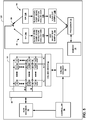
- FIG. 4 is a block diagram of another image sensor that may be used to implement the techniques of this disclosure. Some aspects of the example image sensor 100 depicted in FIG. 4 are similar to the image sensor depicted in FIG. 3 and will not be described in detail again.
- FIG. 4 depicts two ADCs 74A, 74B.
- ADC 74 of FIG. 3 is represented in FIG. 4 as 74A and 74B.
- ADC 74A is a dedicated ADC for converting short exposure time sample S SHORT (i, j)
- ADC 74B is a dedicated ADC for converting long exposure time sample S LONG (i, j).
- processor 76 Upon receiving the converted samples, processor 76 combines the samples in accordance with the techniques described above with particular reference to equations (1)-(3).
- An example image sensor configuration that uses two ADCs, as shown in FIG. 4 may be useful for implementing the techniques of this disclosure because, as described in detail above, two samples, namely short exposure time sample S SHORT (i, j) and long exposure time sample S LONG (i, j) are read out for each pixel cell.
- An image sensor configuration with parallel ADCs, one for converting short exposure time samples and another for converting long exposure time samples, may improve throughput by allowing the short exposure time sample and the long exposure time sample for each pixel cell to be converted substantially simultaneously.
- the example image sensor configuration of FIG. 4 may require additional circuitry as compared to the image sensor configuration depicted in FIG.
- such additional circuitry may, in some implementations, e.g., CMOS backside illumination configurations, be added behind the pixel cell without interfering with the light capturing surface area of the pixel cell. In other words, the additional circuitry will not reduce the pixel cell's fill factor, i.e., the area of the photosensitive semiconductor relative to the area of the pixel cell.
- FIG. 5 is a block diagram of another image sensor that may be used to implement the techniques of this disclosure. Some aspects of the example image sensor 120 depicted in FIG. 5 are similar to the image sensor depicted in FIG. 3 and will not be described in detail again.
- the image sensor in FIG. 5 is similar to the image sensor in FIG. 4 in that two ADCs, one for converting short exposure time sample S SHORT (i, j) and another for converting long exposure time sample S LONG (i, j), are used in parallel, which may improve the throughput to processor 76.
- parallel ADCs 74A and 74B the example configuration depicted in FIG.
- FIG. 5 further includes parallel sample and hold circuitry (70A and 70B) and parallel black level compensation, noise reduction, and amplification circuitry (72A and 72B), which may, in some instances, further improve signal throughput to processor 76.
- the configuration depicted in FIG. 5 includes switch 80 for directing short exposure time sample S SHORT (i, j) for processing through the circuitry generally indicated at 82, and directing long exposure time sample S LONG (i, j) for processing through the circuitry generally indicated at 84.
- processor 76 Upon receiving the converted samples, processor 76 combines the samples in accordance with the techniques described above with particular reference to equations (1)-(3).
- the techniques of this disclosure have been described above with respect to combining only two samples, a short exposure time sample S SHORT (i, j) and a long exposure time sample S LONG (i, j).
- the techniques of this disclosure are not so limited. Rather, the combination scheme described in this disclosure may be used to combine more than two, e.g., five, samples from different exposure times. For example, in order to take a picture of a very bright object, e.g., the sun, a wide dynamic range would be required. As such, more than two images may be necessary in order to achieve that dynamic range. To that end, multiple samples may be collected and combined using the variable weighting techniques described above.
- the even-numbered lines of a pixel cell array e.g., pixel cell array 52 of FIG. 3
- the two different exposures times may be aligned so that they finish at the same time, e.g., substantially simultaneously. Then, the two exposures may be combined to produce an image that is two vertically downsampled images.
- the odd and even lines of the pixel cell array may be constructed and arranged such that they may be independently controlled.
- the image may be downsampled or upsampled in order to generate a value for each spatial location on the pixel cell array for the two different exposures times.
- first exposure time samples may be generated for each of the photosensitive semiconductors on the odd-numbered lines by downsampling or upsampling the samples collected for the even-numbered lines.
- second exposure time samples are generated for each of the photosensitive semiconductors on the even-numbered lines by downsampling or upsampling the samples collected for the odd-numbered lines.
- the first exposure time sample for each of the plurality of spatial locations in each of the plurality of odd-numbered lines are generated by one of downsampling and upsampling the samples collected from the even-numbered lines over the first exposure time
- the second exposure time sample for each of the plurality of spatial locations in each of the plurality of even-numbered lines are generated by one of downsampling and upsampling the samples collected from the odd-numbered lines over the second exposure time.
- the short exposure time samples and long exposure time samples are combined, e.g., using equations (1)-(3). The combination of these samples may produce either a half resolution image or full resolution image that has been upsampled.
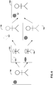
- FIG. 6 depicts a conceptual diagram illustrating the combination of short and long exposure time samples from even and odd-numbered lines using the techniques described above.
- the image depicted at 150 in FIG. 6 illustrates the sensor frame plane with even and odd-numbered line and short and long exposure time control.
- Long exposure time e.g., second exposure time
- samples are collected for the odd-numbered lines and are depicted at 152.
- the long exposure time has caused pixel cells at 153 to become saturated.
- Short exposure time e.g., first exposure time
- samples are collected for the even numbers and are depicted at 154.
- the samples collected for the odd and even-numbered lines are upsampled.
- second exposure time image 156 and first exposure time image are combined to produce a full resolution image, shown at 160.
- the pixel cells at 161 are no longer saturated.
- the two images may be combined on-sensor or off-sensor via an external processor.
- the main difference between combining on-sensor or off-sensor is the amount of additional memory that is needed.
- Combining on the sensor may allow for faster read out of the samples, thereby reducing latency.
- combining on the sensor may allow for reduced data transfers, e.g., reduced bandwidth.
- two frames may need to be read out from the sensor, e.g., a short exposure time frame and a long exposure time frame.
- the data rate must be doubled in order to accommodate the read outs of the two frames.
- the combination is performed on the sensor, the long exposure time frame and short exposure time frame are combined and read out within one frame duration.
- the combination of the long exposure time sample and the short exposure time sample may be performed on-sensor.
- extra memory e.g., a line buffer
- an entire even line may be read out at the short exposure time, converted via an A/D converter, and stored in memory. Then, the entire odd line may be read out at the long exposure time and converted via an A/D converter.
- a processor may retrieve the value from memory for the even line, combine with the converted values for the odd line using the combining techniques described in this disclosure, and then output a single, combined image. Again, using such an on-sensor scheme may reduce the bandwidth needed for the imaging processing pipeline, at the expense of additional memory requirements.
- pixel cell 10 of FIG. 1 may also be used in a sensor, e.g., a CMOS sensor, that utilizes an off-sensor combining scheme.
- a sensor e.g., a CMOS sensor
- the sensor may be reset in the manner described previously, and then the sensor may begin acquiring photons immediately.
- charge may be transferred to capacitor 20.
- correlated double sampling may be used, as described above. Then, samples may be read using a rolling shutter technique.
- correlated double sampling may be performed again.
- the values from the long exposure time may be read out.
- a CCD image sensor may be used in another example imaging technique to produce an HDR image.
- a mechanical shutter may be added to the CCD sensor.
- the mechanical shutter may be opened and the sensor may begin acquiring photons immediately.
- charge, or first sample is transferred to temporary storage region, e.g., a shielded region that may store a copy of the pixel cell.
- the mechanical shutter is closed.
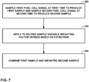
- FIG. 7 is a flow diagram illustrating an example method that may be used to implement the techniques of this disclosure.
- Controller 54 of FIG. 3 samples a first pixel cell signal at a first time, e.g., a short exposure time, to produce a first sample, e.g., S SHORT (i, j), (200).
- Controller 54 also samples a second pixel cell signal at a second time, e.g., a long exposure time, to produce a second sample, e.g., S LONG (i, j) (200).
- the second time is temporally subsequent to the first time.
- the first pixel cell signal and the second pixel cell signal are produced by one of a complementary MOS (CMOS) image sensor and a charge-coupled device (CCD) image sensor.
- CMOS complementary MOS
- CCD charge-coupled device
- Processor 76 of FIG. 3 may apply a variable weighting factor, e.g., M(i, j), to the second sample, wherein the variable weighting factor is defined by a function, e.g., a combining curve C (), at the second sample, e.g., S LONG (i, j) (210).
- the value of M(i, j) is between zero and one, inclusive.
- L, T, K, and ⁇ are described above with respect to equation (4).
- Processor 76 then combines the first sample and the weighted second sample to produce an HDR image (220).
- combining the first sample and the weighted second sample comprises combining the first sample and the weighted second sample on the image sensor, e.g., image sensor 50.
- FIG. 8 is a flow diagram illustrating another example method that may be used to implement the techniques of this disclosure.
- the method of FIG. 8 may be used, for example, with a CCD image sensor.
- a controller opens a mechanical shutter on a CCD image sensor, exposing the image sensor to light (300).
- the controller transfers a first sample developed based on the light to a storage region at a first time (310), and then reads out the first sample from the storage region (320).
- the controller closes the mechanical shutter (330), and a second sample may be transferred to the storage region (340).
- the controller may then read out the second sample from the storage region (350).
- a processor applies a variable weighting factor, e.g., M(i, j), to the second sample (360).
- the processor then combines the first sample and the second weighted sample (370), e.g., by processor 76 to produce a HDR image.
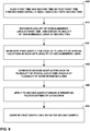
- FIG. 9 is a flow diagram illustrating another example method that may be used to implement the techniques of this disclosure.
- the method of FIG. 9 may be used, for example, with a CMOS image sensor.
- controller 54 of FIG. 3 may align a first exposure time and a second exposure time so that the first exposure time finishes substantially simultaneously with the second exposure time (400).
- Controller 54 may expose a plurality of even-numbered lines of the CMOS image sensor at the first time to produce a first sample for each of a plurality of spatial locations in each of the plurality of even-numbered lines, and may expose a plurality of odd-numbered lines of the CMOS image sensor at the second time to produce the second sample for each of a plurality of spatial locations in each of the plurality of odd-numbered lines (410).
- Processor 76 for example, generates the first sample for each of the plurality of spatial locations in each of the plurality of odd-numbered lines by one of downsampling and upsampling the first sample for each of a plurality of spatial locations in each of the plurality of even-numbered lines (420).
- Processor 76 for example, generates the second sample for each of the plurality of spatial locations in each of the plurality of even-numbered lines by one of downsampling and upsampling the second sample for each of a plurality of spatial locations in each of the plurality of odd-numbered lines (430).
- Processor 76 applies a variable weighting factor, e.g., M(i, j), to the second sample (440).
- Processor 76 then combines the first sample and the second weighted sample to produce a HDR image (450).
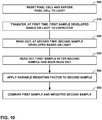
- FIG. 10 is a flow diagram illustrating another example method that may be used to implement the techniques of this disclosure.
- the method of FIG. 10 may be used, for example, with a CMOS image sensor.
- controller 54 of FIG. 3 may reset a photosensitive semiconductor, e.g., photosensitive semiconductor 12, and expose the photosensitive semiconductor to light 54 (500).
- controller 54 may transfer a first sample developed based on the light to a capacitor (510), e.g., capacitor 20 of FIG. 1 .
- controller 54 may read out a second sample developed based on the light from the photosensitive semiconductor (520).
- Controller 54 may read out the first sample after controller 54 reads out the second sample (530).
- Processor 76 may apply a variable weighting factor, e.g., M(i, j), to the second sample (540).
- Processor 76 may combine the first sample and the second weighted sample to produce a HDR image (550).
- a variable weighting factor e.g., M(i, j
- processors including one or more microprocessors, digital signal processors (DSPs), network processors (NPs), application specific integrated circuits (ASICs), field programmable gate arrays (FPGAs), or any other equivalent integrated or discrete logic circuitry, as well as any combinations of such components.
- DSPs digital signal processors
- NPs network processors
- ASICs application specific integrated circuits
- FPGAs field programmable gate arrays
- processors or processing circuitry
- a control unit comprising hardware may also perform one or more of the techniques of this disclosure.
- Such hardware, software, and firmware may be implemented within the same device or within separate devices to support the various operations and functions described in this disclosure.
- any of the described units, modules or components may be implemented together or separately as discrete but interoperable logic devices. Depiction of different features as modules or units is intended to highlight different functional aspects and does not necessarily imply that such modules or units must be realized by separate computing hardware or software components. Rather, functionality associated with one or more modules or units may be performed by separate hardware or software components, or integrated within common or separate hardware or software components.
- Computer readable storage media may include random access memory (RAM), read only memory (ROM), programmable read only memory (PROM), erasable programmable read only memory (EPROM), electronically erasable programmable read only memory (EEPROM), flash memory, a hard disk, a CD-ROM, a floppy disk, a cassette, magnetic media, optical media, or other computer readable media.
- RAM random access memory
- ROM read only memory
- PROM programmable read only memory
- EPROM erasable programmable read only memory
- EEPROM electronically erasable programmable read only memory
- flash memory a hard disk, a CD-ROM, a floppy disk, a cassette, magnetic media, optical media, or other computer readable media.
Landscapes
- Engineering & Computer Science (AREA)
- Multimedia (AREA)
- Signal Processing (AREA)
- Transforming Light Signals Into Electric Signals (AREA)
- Studio Devices (AREA)
- Exposure Control For Cameras (AREA)
Claims (15)
- Procédé comprenant :échantillonner (200), un premier signal de cellule de pixels à un premier temps pour produire un premier échantillon, dénoté par SSHORT;échantillonner (200), un deuxième signal de cellule de pixels à un deuxième temps pour produire un deuxième échantillon, dénoté par SLONG;appliquer (210) un facteur de pondération variable au deuxième échantillon, où le facteur de pondération variable est défini sur la base d'une fonction ; etcombiner (220) le premier échantillon et le deuxième échantillon pondéré conformément à l'équation :

- Procédé selon la revendication 1, dans lequel le premier signal de cellule de pixels est échantillonné à partir d'une cellule de pixels exposée pendant un premier temps d'exposition et dans lequel le deuxième signal de cellule de pixels est échantillonné à partir d'une cellule de pixels différente exposée pendant un deuxième temps d'exposition où le premier temps d'exposition est différent du deuxième temps d'exposition et de préférence où le premier temps d'exposition est plus court que le deuxième temps d'exposition.
- Procédé selon la revendication 1, dans lequel le facteur de pondération pondère des pixels ayant une valeur de luminance inférieure ou égale à une valeur seuil telle que 220 dans une mise en oeuvre de 8 bits plus lourdement que des pixels ayant une valeur de luminance supérieure à la valeur seuil et de préférence en outre dans lequel le facteur de pondération est appliqué seulement au deuxième échantillon.
- Procédé selon la revendication 1, dans lequel la valeur de M(i, j) est d'entre zéro et un, inclus.
- Procédé selon la revendication 1, dans lequel le deuxième temps est temporellement subséquent au premier temps et de préférence dans lequel combiner le premier échantillon et le deuxième échantillon pondéré comprend combiner le premier échantillon et le deuxième échantillon pondéré sur un capteur et dans lequel de préférence en outre le premier signal de cellule de pixels et le deuxième signal de cellule de pixels sont produits par l'un d'entre un capteur d'images MOS complémentaire, CMOS, et un capteur d'images à dispositif à transfert de charge, CCD.
- Procédé selon la revendication 1, dans lequel le premier signal de cellule de pixels et le deuxième signal de cellule de pixels sont produits par un capteur d'images à dispositif à transfert de charge, CCD, et dans lequel échantillonner le premier signal de cellule de pixels au premier temps pour produire le premier échantillon et échantillonner le deuxième signal de cellule de pixels au deuxième temps pour produire le deuxième échantillon comprend :ouvrir un obturateur mécanique sur le capteur d'images CCD et exposer le capteur d'images à la lumière ;transférer le premier échantillon développé sur la base de la lumière à une région de stockage au premier temps;lire le premier échantillon de la région de stockage;fermer l'obturateur mécanique au deuxième temps, le deuxième temps étant temporellement subséquent au premier temps ;transférer le deuxième échantillon à la région de stockage; etlire le deuxième échantillon de la région de stockage.
- Procédé selon la revendication 1, dans lequel le premier signal de cellule de pixels et le deuxième signal de cellule de pixels sont produits par un capteur d'images MOS complémentaire, CMOS, et dans lequel échantillonner le premier signal de cellule de pixels au premier temps pour produire le premier échantillon et échantillonner le deuxième signal de cellule de pixels au deuxième temps pour produire le deuxième échantillon comprend :aligner le premier temps et le deuxième temps de telle sorte que le premier temps finit simultanément avec le deuxième temps ;exposer une pluralité de lignes paires du capteur d'images CMOS au premier temps pour produire le premier échantillon pour chacun d'une pluralité d'emplacements spatiaux dans chacune de la pluralité de lignes paires et exposer une pluralité de lignes impaires du capteur d'images CMOS au deuxième temps pour produire le deuxième échantillon pour chacun d'une pluralité d'emplacements spatiaux dans chacune de la pluralité de lignes impaires ;générer le premier échantillon pour chacun de la pluralité d'emplacements spatiaux dans chacune de la pluralité de lignes impaires en effectuant l'un d'entre sous-échantillonner et sur-échantillonner le premier échantillon pour chacun d'une pluralité d'emplacements spatiaux dans chacune de la pluralité de lignes paires; etgénérer le deuxième échantillon pour chacun de la pluralité d'emplacements spatiaux dans chacune de la pluralité de lignes paires en effectuant l'un d'entre sous-échantillonner et sur-échantillonner le deuxième échantillon pour chacun d'une pluralité d'emplacements spatiaux dans chacune de la pluralité de lignes impaires.
- Procédé selon la revendication 5, dans lequel échantillonner le premier signal de cellule de pixels au premier temps pour produire le premier échantillon et échantillonner le deuxième signal de cellule de pixels au deuxième temps pour produire le deuxième échantillon comprend :remettre une cellule de pixels à l'état initial et exposer la cellule de pixels à la lumière ;transférer, au premier temps, le premier échantillon développé sur la base de la lumière à un condensateur ;lire, au deuxième temps, le deuxième échantillon sur la base de la lumière ; etlire le premier échantillon après que le deuxième échantillon a été lu.
- Système comprenant :un moyen pour échantillonner (70A), un premier signal de cellule de pixels à un premier temps pour produire un premier échantillon, dénoté par SSHORT;un moyen pour échantillonner (70B), un deuxième signal de cellule de pixels à un deuxième temps pour produire un deuxième échantillon, dénoté par SLONG;un moyen pour appliquer (76) un facteur de pondération variable au deuxième échantillon, où le facteur de pondération variable est défini sur la base d'une fonction; etun moyen pour combiner (76) le premier échantillon et le deuxième échantillon pondéré conformément à l'équation :

- Système selon la revendication 9, dans lequel la valeur de M(i, j) est d'entre zéro et un, inclus.
- Système selon la revendication 9, dans lequel le deuxième temps est temporellement subséquent au premier temps et de préférence dans lequel le moyen pour combiner le premier échantillon et le deuxième échantillon pondéré comprend un moyen pour combiner le premier échantillon et le deuxième échantillon pondéré sur un capteur et dans lequel de préférence en outre le premier signal de cellule de pixels et le deuxième signal de cellule de pixels sont produits par l'un d'entre un capteur d'images MOS complémentaire, CMOS, et un capteur d'images à dispositif à transfert de charge, CCD.
- Système selon la revendication 9, dans lequel le premier signal de cellule de pixels et le deuxième signal de cellule de pixels sont produits par un capteur d'images à dispositif à transfert de charge, CCD, et dans lequel le moyen pour échantillonner le premier signal de cellule de pixels au premier temps pour produire le premier échantillon et le moyen pour échantillonner le deuxième signal de cellule de pixels au deuxième temps pour produire le deuxième échantillon comprend :un moyen pour ouvrir un obturateur mécanique sur le capteur d'images CCD et exposer le capteur d'images à la lumière ;un moyen pour transférer le premier échantillon développé sur la base de la lumière à une région de stockage au premier temps ;un moyen pour lire le premier échantillon de la région de stockage;un moyen pour fermer l'obturateur mécanique au deuxième temps, le deuxième temps étant temporellement subséquent au premier temps ;un moyen pour transférer le deuxième échantillon à la région de stockage; etun moyen pour lire le deuxième échantillon de la région de stockage.
- Système selon la revendication 9, dans lequel le premier signal de cellule de pixels et le deuxième signal de cellule de pixels sont produits par un capteur d'images MOS complémentaire, CMOS, et dans lequel le moyen pour échantillonner le premier signal de cellule de pixels au premier temps pour produire le premier échantillon et le moyen pour échantillonner le deuxième signal de cellule de pixels au deuxième temps pour produire le deuxième échantillon comprend :un moyen pour aligner le premier temps et le deuxième temps de telle sorte que le premier temps finit simultanément avec le deuxième temps ;un moyen pour exposer une pluralité de lignes paires du capteur d'images CMOS au premier temps pour produire le premier échantillon pour chacun d'une pluralité d'emplacements spatiaux dans chacune de la pluralité de lignes paires et exposer une pluralité de lignes impaires du capteur d'images CMOS au deuxième temps pour produire le deuxième échantillon pour chacun d'une pluralité d'emplacements spatiaux dans chacune de la pluralité de lignes impaires;un moyen pour générer le premier échantillon pour chacun de la pluralité d'emplacements spatiaux dans chacune de la pluralité de lignes impaires en effectuant l'un d'entre sous-échantillonner et sur-échantillonner le premier échantillon pour chacun d'une pluralité d'emplacements spatiaux dans chacune de la pluralité de lignes paires; etun moyen pour générer le deuxième échantillon pour chacun de la pluralité d'emplacements spatiaux dans chacune de la pluralité de lignes paires en effectuant l'un d'entre sous-échantillonner et sur-échantillonner le deuxième échantillon pour chacun d'une pluralité d'emplacements spatiaux dans chacune de la pluralité de lignes impaires.
- Système selon la revendication 9, dans lequel le moyen pour échantillonner le premier signal de cellule de pixels au premier temps pour produire le premier échantillon et le moyen pour échantillonner le deuxième signal de cellule de pixels au deuxième temps pour produire le deuxième échantillon comprend :un moyen pour remettre une cellule de pixels à l'état initial et exposer la cellule de pixels à la lumière ;un moyen pour transférer, au premier temps, le premier échantillon développé sur la base de la lumière à un condensateur ;un moyen pour lire, au deuxième temps, le deuxième échantillon sur la base de la lumière ; etun moyen pour lire le premier échantillon après que le deuxième échantillon a été lu.
- Support lisible par ordinateur comprenant des instructions qui, lorsque exécutées par un ou plusieurs processeurs, font que l'un ou les plusieurs processeurs exécutent le procédé selon l'une quelconque des revendications 1 à 8.
Applications Claiming Priority (2)
| Application Number | Priority Date | Filing Date | Title |
|---|---|---|---|
| US12/873,981 US8994843B2 (en) | 2010-09-01 | 2010-09-01 | High dynamic range image sensor |
| PCT/US2011/050068 WO2012031026A2 (fr) | 2010-09-01 | 2011-08-31 | Capteur d'images à plage dynamique étendue |
Publications (2)
| Publication Number | Publication Date |
|---|---|
| EP2612492A2 EP2612492A2 (fr) | 2013-07-10 |
| EP2612492B1 true EP2612492B1 (fr) | 2018-01-10 |
Family
ID=44675825
Family Applications (1)
| Application Number | Title | Priority Date | Filing Date |
|---|---|---|---|
| EP11760911.5A Not-in-force EP2612492B1 (fr) | 2010-09-01 | 2011-08-31 | Capteur d'images à plage dynamique étendue |
Country Status (6)
| Country | Link |
|---|---|
| US (1) | US8994843B2 (fr) |
| EP (1) | EP2612492B1 (fr) |
| JP (2) | JP2013537020A (fr) |
| KR (1) | KR101473597B1 (fr) |
| CN (1) | CN103141081B (fr) |
| WO (1) | WO2012031026A2 (fr) |
Families Citing this family (30)
| Publication number | Priority date | Publication date | Assignee | Title |
|---|---|---|---|---|
| KR101665511B1 (ko) * | 2010-02-11 | 2016-10-12 | 삼성전자 주식회사 | 광역 역광 보정 하드웨어 장치 및 이를 포함하는 촬영 장치 |
| JP6021465B2 (ja) * | 2011-07-11 | 2016-11-09 | キヤノン株式会社 | 画像処理装置及び画像処理装置の制御方法 |
| US9338372B2 (en) * | 2012-09-19 | 2016-05-10 | Semiconductor Components Industries, Llc | Column-based high dynamic range imaging systems |
| US10368053B2 (en) | 2012-11-14 | 2019-07-30 | Qualcomm Incorporated | Structured light active depth sensing systems combining multiple images to compensate for differences in reflectivity and/or absorption |
| US9437171B2 (en) | 2012-12-05 | 2016-09-06 | Texas Instruments Incorporated | Local tone mapping for high dynamic range images |
| US8866927B2 (en) | 2012-12-13 | 2014-10-21 | Google Inc. | Determining an image capture payload burst structure based on a metering image capture sweep |
| US9087391B2 (en) | 2012-12-13 | 2015-07-21 | Google Inc. | Determining an image capture payload burst structure |
| US8866928B2 (en) | 2012-12-18 | 2014-10-21 | Google Inc. | Determining exposure times using split paxels |
| US9247152B2 (en) | 2012-12-20 | 2016-01-26 | Google Inc. | Determining image alignment failure |
| US9686537B2 (en) | 2013-02-05 | 2017-06-20 | Google Inc. | Noise models for image processing |
| US9117134B1 (en) | 2013-03-19 | 2015-08-25 | Google Inc. | Image merging with blending |
| US9066017B2 (en) | 2013-03-25 | 2015-06-23 | Google Inc. | Viewfinder display based on metering images |
| US9077913B2 (en) | 2013-05-24 | 2015-07-07 | Google Inc. | Simulating high dynamic range imaging with virtual long-exposure images |
| US9131201B1 (en) | 2013-05-24 | 2015-09-08 | Google Inc. | Color correcting virtual long exposures with true long exposures |
| TWI464526B (zh) * | 2013-08-08 | 2014-12-11 | Quanta Comp Inc | 高動態範圍影像曝光時間控制方法 |
| US9615012B2 (en) | 2013-09-30 | 2017-04-04 | Google Inc. | Using a second camera to adjust settings of first camera |
| KR102149187B1 (ko) * | 2014-02-21 | 2020-08-28 | 삼성전자주식회사 | 전자 장치와, 그의 제어 방법 |
| KR102191245B1 (ko) * | 2014-06-20 | 2020-12-15 | 삼성전자주식회사 | 이미지 센서 구동 방법, 이를 채용한 이미지 센서 및 이를 포함하는 휴대용 전자 기기 |
| JP6299544B2 (ja) * | 2014-09-24 | 2018-03-28 | 株式会社Jvcケンウッド | 固体撮像装置 |
| KR102273656B1 (ko) * | 2014-11-24 | 2021-07-05 | 삼성전자주식회사 | 광역 역광 보정 영상의 노이즈 레벨 제어 장치, 및 이를 포함하는 영상 처리 시스템 |
| US9843737B2 (en) * | 2015-01-22 | 2017-12-12 | Panasonic Intellectual Property Management Co., Ltd. | Imaging device |
| KR20160138685A (ko) | 2015-05-26 | 2016-12-06 | 에스케이하이닉스 주식회사 | 저 복잡도의 하이 다이나믹 레인지 이미지 생성 장치 및 그 방법 |
| JP2017055248A (ja) | 2015-09-09 | 2017-03-16 | ルネサスエレクトロニクス株式会社 | 撮像素子 |
| KR20190114332A (ko) | 2018-03-29 | 2019-10-10 | 에스케이하이닉스 주식회사 | 이미지 센싱 장치 및 그의 동작 방법 |
| JP7130777B2 (ja) | 2018-06-07 | 2022-09-05 | ドルビー ラボラトリーズ ライセンシング コーポレイション | シングルショットhdrカラーイメージセンサからのhdr画像生成 |
| KR102648747B1 (ko) * | 2019-01-18 | 2024-03-20 | 삼성전자주식회사 | Hdr 이미지를 생성하기 위한 이미징 시스템 및 그것의 동작 방법 |
| CN109951656B (zh) * | 2019-04-23 | 2022-03-08 | Oppo广东移动通信有限公司 | 一种图像传感器和电子设备 |
| US10855931B1 (en) * | 2019-11-07 | 2020-12-01 | Novatek Microelectronics Corp. | High dynamic range image sensing method for image sensing device |
| DE102020123671B4 (de) | 2020-09-10 | 2022-12-22 | Ifm Electronic Gmbh | Verfahren und Vorrichtung zur Dynamikerweiterung eines Lichtlaufzeitkamerasystems |
| JP2023036384A (ja) * | 2021-09-02 | 2023-03-14 | ソニーセミコンダクタソリューションズ株式会社 | 固体撮像装置 |
Citations (1)
| Publication number | Priority date | Publication date | Assignee | Title |
|---|---|---|---|---|
| EP1819151A1 (fr) * | 2006-02-09 | 2007-08-15 | Sony Corporation | Dispositif d'imagerie à l'état solide, procédé de contrôle d'un dispositif d'imagerie à l'état solide et caméra |
Family Cites Families (30)
| Publication number | Priority date | Publication date | Assignee | Title |
|---|---|---|---|---|
| US5471515A (en) | 1994-01-28 | 1995-11-28 | California Institute Of Technology | Active pixel sensor with intra-pixel charge transfer |
| DE69628187D1 (de) | 1995-11-07 | 2003-06-18 | California Inst Of Techn | Bildsensor mit linearem ausgang mit grossem dynamikbereich |
| JP3755175B2 (ja) * | 1995-12-25 | 2006-03-15 | ソニー株式会社 | 固体撮像装置 |
| JPH1023324A (ja) | 1996-07-03 | 1998-01-23 | Matsushita Electric Ind Co Ltd | 撮像装置 |
| JP2000050151A (ja) * | 1998-07-28 | 2000-02-18 | Olympus Optical Co Ltd | 撮像装置 |
| JP4337177B2 (ja) | 1999-07-09 | 2009-09-30 | ソニー株式会社 | 固体撮像素子およびその駆動方法 |
| JP2001069408A (ja) | 1999-08-30 | 2001-03-16 | Sony Corp | 固体撮像素子およびその駆動方法ならびにカメラシステム |
| US7023479B2 (en) * | 2000-05-16 | 2006-04-04 | Canon Kabushiki Kaisha | Image input apparatus having addition and subtraction processing |
| US7050094B2 (en) * | 2000-10-26 | 2006-05-23 | Micron Technology, Inc. | Wide dynamic range operation for CMOS sensor with freeze-frame shutter |
| JP3731729B2 (ja) | 2000-12-20 | 2006-01-05 | 松下電器産業株式会社 | 画像合成回路 |
| JP2003219281A (ja) | 2002-01-18 | 2003-07-31 | Sony Corp | 撮像装置およびそのシャッタ駆動方法 |
| JP4272443B2 (ja) | 2003-02-05 | 2009-06-03 | パナソニック株式会社 | 画像処理装置および画像処理方法 |
| US7019277B2 (en) | 2003-03-13 | 2006-03-28 | Psion Teklogix Systems Inc. | Imaging device |
| KR100810310B1 (ko) * | 2003-08-29 | 2008-03-07 | 삼성전자주식회사 | 조도차가 다른 영상의 재구성 장치 및 방법 |
| JP4421353B2 (ja) | 2004-04-01 | 2010-02-24 | 浜松ホトニクス株式会社 | 固体撮像装置 |
| WO2005107240A1 (fr) * | 2004-04-28 | 2005-11-10 | Chuo Electronics Co., Ltd. | Procede et appareil d'imagerie automatique |
| EP1641249A1 (fr) | 2004-09-27 | 2006-03-29 | STMicroelectronics Limited | Améliorations relatives à des capteurs d'images |
| US7259413B2 (en) | 2004-09-28 | 2007-08-21 | Micron Technology, Inc. | High dynamic range image sensor |
| CA2511220C (fr) | 2005-03-21 | 2012-08-14 | Sunnybrook Technologies Inc. | Methodes et appareil d'exposition multiple pour appareils photos electroniques |
| JP4855704B2 (ja) * | 2005-03-31 | 2012-01-18 | 株式会社東芝 | 固体撮像装置 |
| US7750960B2 (en) | 2006-03-15 | 2010-07-06 | Honeywell International Inc. | System and apparatus for high dynamic range sensor |
| JP4998056B2 (ja) | 2006-05-11 | 2012-08-15 | セイコーエプソン株式会社 | 撮像装置、撮像システム及び撮像方法 |
| JP2008042828A (ja) * | 2006-08-10 | 2008-02-21 | Matsushita Electric Ind Co Ltd | 固体撮像素子及びその駆動方法。 |
| JP4961982B2 (ja) | 2006-12-07 | 2012-06-27 | ソニー株式会社 | 固体撮像装置、固体撮像装置の駆動方法および撮像装置 |
| US7825969B2 (en) * | 2006-12-15 | 2010-11-02 | Nokia Corporation | Image stabilization using multi-exposure pattern |
| US7616243B2 (en) * | 2007-03-07 | 2009-11-10 | Altasens, Inc. | Method and apparatus for improving and controlling dynamic range in an image sensor |
| JP2008277894A (ja) | 2007-04-25 | 2008-11-13 | Matsushita Electric Ind Co Ltd | 撮像装置、撮像方法および集積回路 |
| JP4438847B2 (ja) * | 2007-09-28 | 2010-03-24 | ソニー株式会社 | 撮像装置、撮像制御方法及び撮像制御プログラム |
| US7777804B2 (en) | 2007-10-26 | 2010-08-17 | Omnivision Technologies, Inc. | High dynamic range sensor with reduced line memory for color interpolation |
| JP2010136078A (ja) * | 2008-12-04 | 2010-06-17 | Fujifilm Corp | 撮像装置及びその駆動制御方法 |
-
2010
- 2010-09-01 US US12/873,981 patent/US8994843B2/en active Active
-
2011
- 2011-08-31 KR KR1020137008243A patent/KR101473597B1/ko active Active
- 2011-08-31 EP EP11760911.5A patent/EP2612492B1/fr not_active Not-in-force
- 2011-08-31 WO PCT/US2011/050068 patent/WO2012031026A2/fr not_active Ceased
- 2011-08-31 CN CN201180046572.8A patent/CN103141081B/zh active Active
- 2011-08-31 JP JP2013527289A patent/JP2013537020A/ja not_active Withdrawn
-
2015
- 2015-12-11 JP JP2015242442A patent/JP2016096558A/ja active Pending
Patent Citations (1)
| Publication number | Priority date | Publication date | Assignee | Title |
|---|---|---|---|---|
| EP1819151A1 (fr) * | 2006-02-09 | 2007-08-15 | Sony Corporation | Dispositif d'imagerie à l'état solide, procédé de contrôle d'un dispositif d'imagerie à l'état solide et caméra |
Also Published As
| Publication number | Publication date |
|---|---|
| WO2012031026A2 (fr) | 2012-03-08 |
| CN103141081B (zh) | 2016-12-07 |
| KR101473597B1 (ko) | 2014-12-24 |
| US20120050557A1 (en) | 2012-03-01 |
| US8994843B2 (en) | 2015-03-31 |
| JP2016096558A (ja) | 2016-05-26 |
| CN103141081A (zh) | 2013-06-05 |
| WO2012031026A3 (fr) | 2013-01-03 |
| KR20130049825A (ko) | 2013-05-14 |
| JP2013537020A (ja) | 2013-09-26 |
| EP2612492A2 (fr) | 2013-07-10 |
Similar Documents
| Publication | Publication Date | Title |
|---|---|---|
| EP2612492B1 (fr) | Capteur d'images à plage dynamique étendue | |
| US8134624B2 (en) | Method and apparatus providing multiple exposure high dynamic range sensor | |
| TWI424742B (zh) | 用於像素單元之高動態運作之方法及裝置 | |
| US9554071B2 (en) | Method and apparatus providing pixel storage gate charge sensing for electronic stabilization in imagers | |
| US8330843B2 (en) | Solid-state image sensing device, method for driving solid-state image sensing device, and image sensing system incorporated with solid-state image sensing device | |
| US8610811B2 (en) | Image pickup apparatus | |
| US8482644B2 (en) | Solid-state imaging device | |
| US20090073293A1 (en) | CMOS image sensors with increased dynamic range and methods of operating the same | |
| US10033956B2 (en) | Image sensor | |
| TW200529658A (en) | Method of controlling semiconductor device, signal processing method, semiconductor device, and electronic apparatus | |
| WO2018118016A1 (fr) | Schéma d'obturateur global réduisant les effets d'un courant d'obscurité | |
| US20090059039A1 (en) | Method and apparatus for combining multi-exposure image data | |
| US10051216B2 (en) | Imaging apparatus and imaging method thereof using correlated double sampling | |
| US20040239781A1 (en) | Image capture apparatus | |
| JP2003259234A (ja) | Cmosイメージセンサ | |
| US20110007201A1 (en) | Solid state imaging device suppressing blooming | |
| JP2007013362A (ja) | 撮像装置及び撮像方法 |
Legal Events
| Date | Code | Title | Description |
|---|---|---|---|
| PUAI | Public reference made under article 153(3) epc to a published international application that has entered the european phase |
Free format text: ORIGINAL CODE: 0009012 |
|
| 17P | Request for examination filed |
Effective date: 20130304 |
|
| AK | Designated contracting states |
Kind code of ref document: A2 Designated state(s): AL AT BE BG CH CY CZ DE DK EE ES FI FR GB GR HR HU IE IS IT LI LT LU LV MC MK MT NL NO PL PT RO RS SE SI SK SM TR |
|
| DAX | Request for extension of the european patent (deleted) | ||
| 17Q | First examination report despatched |
Effective date: 20161219 |
|
| GRAP | Despatch of communication of intention to grant a patent |
Free format text: ORIGINAL CODE: EPIDOSNIGR1 |
|
| RIC1 | Information provided on ipc code assigned before grant |
Ipc: H04N 5/3745 20110101ALN20170630BHEP Ipc: H04N 5/355 20110101AFI20170630BHEP |
|
| INTG | Intention to grant announced |
Effective date: 20170727 |
|
| GRAS | Grant fee paid |
Free format text: ORIGINAL CODE: EPIDOSNIGR3 |
|
| GRAA | (expected) grant |
Free format text: ORIGINAL CODE: 0009210 |
|
| AK | Designated contracting states |
Kind code of ref document: B1 Designated state(s): AL AT BE BG CH CY CZ DE DK EE ES FI FR GB GR HR HU IE IS IT LI LT LU LV MC MK MT NL NO PL PT RO RS SE SI SK SM TR |
|
| REG | Reference to a national code |
Ref country code: CH Ref legal event code: EP Ref country code: AT Ref legal event code: REF Ref document number: 963640 Country of ref document: AT Kind code of ref document: T Effective date: 20180115 |
|
| REG | Reference to a national code |
Ref country code: IE Ref legal event code: FG4D |
|
| REG | Reference to a national code |
Ref country code: DE Ref legal event code: R096 Ref document number: 602011044947 Country of ref document: DE |
|
| REG | Reference to a national code |
Ref country code: NL Ref legal event code: MP Effective date: 20180110 |
|
| REG | Reference to a national code |
Ref country code: AT Ref legal event code: MK05 Ref document number: 963640 Country of ref document: AT Kind code of ref document: T Effective date: 20180110 |
|
| PG25 | Lapsed in a contracting state [announced via postgrant information from national office to epo] |
Ref country code: NL Free format text: LAPSE BECAUSE OF FAILURE TO SUBMIT A TRANSLATION OF THE DESCRIPTION OR TO PAY THE FEE WITHIN THE PRESCRIBED TIME-LIMIT Effective date: 20180110 |
|
| REG | Reference to a national code |
Ref country code: FR Ref legal event code: PLFP Year of fee payment: 8 |
|
| PG25 | Lapsed in a contracting state [announced via postgrant information from national office to epo] |
Ref country code: HR Free format text: LAPSE BECAUSE OF FAILURE TO SUBMIT A TRANSLATION OF THE DESCRIPTION OR TO PAY THE FEE WITHIN THE PRESCRIBED TIME-LIMIT Effective date: 20180110 Ref country code: CY Free format text: LAPSE BECAUSE OF FAILURE TO SUBMIT A TRANSLATION OF THE DESCRIPTION OR TO PAY THE FEE WITHIN THE PRESCRIBED TIME-LIMIT Effective date: 20180110 Ref country code: ES Free format text: LAPSE BECAUSE OF FAILURE TO SUBMIT A TRANSLATION OF THE DESCRIPTION OR TO PAY THE FEE WITHIN THE PRESCRIBED TIME-LIMIT Effective date: 20180110 Ref country code: LT Free format text: LAPSE BECAUSE OF FAILURE TO SUBMIT A TRANSLATION OF THE DESCRIPTION OR TO PAY THE FEE WITHIN THE PRESCRIBED TIME-LIMIT Effective date: 20180110 Ref country code: NO Free format text: LAPSE BECAUSE OF FAILURE TO SUBMIT A TRANSLATION OF THE DESCRIPTION OR TO PAY THE FEE WITHIN THE PRESCRIBED TIME-LIMIT Effective date: 20180410 Ref country code: FI Free format text: LAPSE BECAUSE OF FAILURE TO SUBMIT A TRANSLATION OF THE DESCRIPTION OR TO PAY THE FEE WITHIN THE PRESCRIBED TIME-LIMIT Effective date: 20180110 |
|
| PG25 | Lapsed in a contracting state [announced via postgrant information from national office to epo] |
Ref country code: AT Free format text: LAPSE BECAUSE OF FAILURE TO SUBMIT A TRANSLATION OF THE DESCRIPTION OR TO PAY THE FEE WITHIN THE PRESCRIBED TIME-LIMIT Effective date: 20180110 Ref country code: LV Free format text: LAPSE BECAUSE OF FAILURE TO SUBMIT A TRANSLATION OF THE DESCRIPTION OR TO PAY THE FEE WITHIN THE PRESCRIBED TIME-LIMIT Effective date: 20180110 Ref country code: SE Free format text: LAPSE BECAUSE OF FAILURE TO SUBMIT A TRANSLATION OF THE DESCRIPTION OR TO PAY THE FEE WITHIN THE PRESCRIBED TIME-LIMIT Effective date: 20180110 Ref country code: PL Free format text: LAPSE BECAUSE OF FAILURE TO SUBMIT A TRANSLATION OF THE DESCRIPTION OR TO PAY THE FEE WITHIN THE PRESCRIBED TIME-LIMIT Effective date: 20180110 Ref country code: GR Free format text: LAPSE BECAUSE OF FAILURE TO SUBMIT A TRANSLATION OF THE DESCRIPTION OR TO PAY THE FEE WITHIN THE PRESCRIBED TIME-LIMIT Effective date: 20180411 Ref country code: IS Free format text: LAPSE BECAUSE OF FAILURE TO SUBMIT A TRANSLATION OF THE DESCRIPTION OR TO PAY THE FEE WITHIN THE PRESCRIBED TIME-LIMIT Effective date: 20180510 Ref country code: RS Free format text: LAPSE BECAUSE OF FAILURE TO SUBMIT A TRANSLATION OF THE DESCRIPTION OR TO PAY THE FEE WITHIN THE PRESCRIBED TIME-LIMIT Effective date: 20180110 Ref country code: BG Free format text: LAPSE BECAUSE OF FAILURE TO SUBMIT A TRANSLATION OF THE DESCRIPTION OR TO PAY THE FEE WITHIN THE PRESCRIBED TIME-LIMIT Effective date: 20180410 |
|
| REG | Reference to a national code |
Ref country code: DE Ref legal event code: R097 Ref document number: 602011044947 Country of ref document: DE |
|
| PG25 | Lapsed in a contracting state [announced via postgrant information from national office to epo] |
Ref country code: AL Free format text: LAPSE BECAUSE OF FAILURE TO SUBMIT A TRANSLATION OF THE DESCRIPTION OR TO PAY THE FEE WITHIN THE PRESCRIBED TIME-LIMIT Effective date: 20180110 Ref country code: EE Free format text: LAPSE BECAUSE OF FAILURE TO SUBMIT A TRANSLATION OF THE DESCRIPTION OR TO PAY THE FEE WITHIN THE PRESCRIBED TIME-LIMIT Effective date: 20180110 Ref country code: RO Free format text: LAPSE BECAUSE OF FAILURE TO SUBMIT A TRANSLATION OF THE DESCRIPTION OR TO PAY THE FEE WITHIN THE PRESCRIBED TIME-LIMIT Effective date: 20180110 Ref country code: IT Free format text: LAPSE BECAUSE OF FAILURE TO SUBMIT A TRANSLATION OF THE DESCRIPTION OR TO PAY THE FEE WITHIN THE PRESCRIBED TIME-LIMIT Effective date: 20180110 |
|
| PLBE | No opposition filed within time limit |
Free format text: ORIGINAL CODE: 0009261 |
|
| STAA | Information on the status of an ep patent application or granted ep patent |
Free format text: STATUS: NO OPPOSITION FILED WITHIN TIME LIMIT |
|
| PG25 | Lapsed in a contracting state [announced via postgrant information from national office to epo] |
Ref country code: SM Free format text: LAPSE BECAUSE OF FAILURE TO SUBMIT A TRANSLATION OF THE DESCRIPTION OR TO PAY THE FEE WITHIN THE PRESCRIBED TIME-LIMIT Effective date: 20180110 Ref country code: CZ Free format text: LAPSE BECAUSE OF FAILURE TO SUBMIT A TRANSLATION OF THE DESCRIPTION OR TO PAY THE FEE WITHIN THE PRESCRIBED TIME-LIMIT Effective date: 20180110 Ref country code: DK Free format text: LAPSE BECAUSE OF FAILURE TO SUBMIT A TRANSLATION OF THE DESCRIPTION OR TO PAY THE FEE WITHIN THE PRESCRIBED TIME-LIMIT Effective date: 20180110 Ref country code: SK Free format text: LAPSE BECAUSE OF FAILURE TO SUBMIT A TRANSLATION OF THE DESCRIPTION OR TO PAY THE FEE WITHIN THE PRESCRIBED TIME-LIMIT Effective date: 20180110 |
|
| 26N | No opposition filed |
Effective date: 20181011 |
|
| PG25 | Lapsed in a contracting state [announced via postgrant information from national office to epo] |
Ref country code: SI Free format text: LAPSE BECAUSE OF FAILURE TO SUBMIT A TRANSLATION OF THE DESCRIPTION OR TO PAY THE FEE WITHIN THE PRESCRIBED TIME-LIMIT Effective date: 20180110 |
|
| PG25 | Lapsed in a contracting state [announced via postgrant information from national office to epo] |
Ref country code: MC Free format text: LAPSE BECAUSE OF FAILURE TO SUBMIT A TRANSLATION OF THE DESCRIPTION OR TO PAY THE FEE WITHIN THE PRESCRIBED TIME-LIMIT Effective date: 20180110 |
|
| REG | Reference to a national code |
Ref country code: CH Ref legal event code: PL |
|
| PG25 | Lapsed in a contracting state [announced via postgrant information from national office to epo] |
Ref country code: LU Free format text: LAPSE BECAUSE OF NON-PAYMENT OF DUE FEES Effective date: 20180831 Ref country code: LI Free format text: LAPSE BECAUSE OF NON-PAYMENT OF DUE FEES Effective date: 20180831 Ref country code: CH Free format text: LAPSE BECAUSE OF NON-PAYMENT OF DUE FEES Effective date: 20180831 |
|
| REG | Reference to a national code |
Ref country code: BE Ref legal event code: MM Effective date: 20180831 |
|
| PG25 | Lapsed in a contracting state [announced via postgrant information from national office to epo] |
Ref country code: BE Free format text: LAPSE BECAUSE OF NON-PAYMENT OF DUE FEES Effective date: 20180831 |
|
| PG25 | Lapsed in a contracting state [announced via postgrant information from national office to epo] |
Ref country code: MT Free format text: LAPSE BECAUSE OF NON-PAYMENT OF DUE FEES Effective date: 20180831 |
|
| PG25 | Lapsed in a contracting state [announced via postgrant information from national office to epo] |
Ref country code: TR Free format text: LAPSE BECAUSE OF FAILURE TO SUBMIT A TRANSLATION OF THE DESCRIPTION OR TO PAY THE FEE WITHIN THE PRESCRIBED TIME-LIMIT Effective date: 20180110 |
|
| PG25 | Lapsed in a contracting state [announced via postgrant information from national office to epo] |
Ref country code: PT Free format text: LAPSE BECAUSE OF FAILURE TO SUBMIT A TRANSLATION OF THE DESCRIPTION OR TO PAY THE FEE WITHIN THE PRESCRIBED TIME-LIMIT Effective date: 20180110 Ref country code: HU Free format text: LAPSE BECAUSE OF FAILURE TO SUBMIT A TRANSLATION OF THE DESCRIPTION OR TO PAY THE FEE WITHIN THE PRESCRIBED TIME-LIMIT; INVALID AB INITIO Effective date: 20110831 |
|
| PG25 | Lapsed in a contracting state [announced via postgrant information from national office to epo] |
Ref country code: IE Free format text: LAPSE BECAUSE OF NON-PAYMENT OF DUE FEES Effective date: 20180831 Ref country code: MK Free format text: LAPSE BECAUSE OF NON-PAYMENT OF DUE FEES Effective date: 20180110 |
|
| REG | Reference to a national code |
Ref country code: DE Ref legal event code: R079 Ref document number: 602011044947 Country of ref document: DE Free format text: PREVIOUS MAIN CLASS: H04N0005355000 Ipc: H04N0025570000 |
|
| PGFP | Annual fee paid to national office [announced via postgrant information from national office to epo] |
Ref country code: GB Payment date: 20230712 Year of fee payment: 13 |
|
| PGFP | Annual fee paid to national office [announced via postgrant information from national office to epo] |
Ref country code: FR Payment date: 20230710 Year of fee payment: 13 Ref country code: DE Payment date: 20230711 Year of fee payment: 13 |
|
| REG | Reference to a national code |
Ref country code: DE Ref legal event code: R119 Ref document number: 602011044947 Country of ref document: DE |
|
| GBPC | Gb: european patent ceased through non-payment of renewal fee |
Effective date: 20240831 |
|
| PG25 | Lapsed in a contracting state [announced via postgrant information from national office to epo] |
Ref country code: DE Free format text: LAPSE BECAUSE OF NON-PAYMENT OF DUE FEES Effective date: 20250301 |
|
| PG25 | Lapsed in a contracting state [announced via postgrant information from national office to epo] |
Ref country code: GB Free format text: LAPSE BECAUSE OF NON-PAYMENT OF DUE FEES Effective date: 20240831 |
|
| PG25 | Lapsed in a contracting state [announced via postgrant information from national office to epo] |
Ref country code: FR Free format text: LAPSE BECAUSE OF NON-PAYMENT OF DUE FEES Effective date: 20240831 |